LM2694 30V, 600 mA Step Down Switching RegulatorCheck for Samples: LM2694
1FEATURES DESCRIPTIONThe LM2694 Step Down Switching Regulator features
2• Integrated N-Channel Buck Switchall of the functions needed to implement a low cost,
• Integrated Start-Up Regulator efficient, buck bias regulator capable of supplying• Input Voltage Range: 8V to 30V 0.6A to the load. This buck regulator contains an N-
Channel Buck Switch, and is available in the 3 x 3• No Loop Compensation Requiredthermally enhanced WSON-10 package and a• Ultra-Fast Transient Response TSSOP-14 package. The feedback regulation
• Operating Frequency Remains Constant with scheme requires no loop compensation, results inLoad Current and Input Voltage Variations fast load transient response, and simplifies circuit
implementation. The operating frequency remains• Maximum Duty Cycle Limited During Start-Upconstant with line and load variations due to the• Adjustable Output Voltage inverse relationship between the input voltage and
• Valley Current Limit At 0.6A the on-time. The valley current limit results in asmooth transition from constant voltage to constant• Maximum Switching Frequency: 1 MHzcurrent mode when current limit is detected, reducing• Precision Internal Referencethe frequency and output voltage, without the use of
• Low Bias Current foldback. Additional features include: VCC under-voltage lockout, thermal shutdown, gate drive under-• Highly Efficient Operationvoltage lockout, and maximum duty cycle limiter.• Thermal Shutdown
PackageTYPICAL APPLICATIONS• WSON-10 (3 mm x 3 mm) w/Exposed Pad
• High Efficiency Point-Of-Load (POL) Regulator• TSSOP-14
• Non-Isolated Telecommunication BuckRegulator
• Secondary High Voltage Post Regulator
Basic Step Down Regulator
1
Please be aware that an important notice concerning availability, standard warranty, and use in critical applications ofTexas Instruments semiconductor products and disclaimers thereto appears at the end of this data sheet.
2All trademarks are the property of their respective owners.
Figure 1. 14-Lead TSSOP Package Figure 2. 10-Lead WSON PackageSee Package Number PW0014A See Package Number DSC0010A
Pin DescriptionsPIN NUMBER
NAME DESCRIPTION APPLICATION INFORMATIONWSON-10 TSSOP-14
1 2 SW Switching Node Internally connected to the buck switch source.Connect to the inductor, free-wheeling diode, andbootstrap capacitor.
2 3 BST Boost pin for bootstrap capacitor Connect a 0.022 µF capacitor from SW to the BSTpin. The capacitor is charged from VCC via aninternal diode during the buck switch off-time.
3 4 ISEN Current sense During the buck switch off-time, the inductor currentflows through the internal sense resistor, and out ofthe ISEN pin to the free-wheeling diode. The currentlimit is nominally set at 0.62A.
4 5 SGND Current Sense Ground Re-circulating current flows into this pin to the currentsense resistor.
5 6 RTN Circuit Ground Ground return for all internal circuitry other than thecurrent sense resistor.
6 9 FB Voltage feedback input from the Input to both the regulation and over-voltageregulated output comparators. The FB pin regulation level is 2.5V.
7 10 SS Softstart An internal current source charges the SS pincapacitor to 2.5V to soft-start the reference input ofthe regulation comparator.
8 11 RON/SD On-time control and shutdown An external resistor from VIN to the RON/SD pin setsthe buck switch on-time. Grounding this pin shutsdown the regulator.
9 12 VCC Output of the startup regulator The voltage at VCC is nominally regulated at 7V.Connect a 0.1 µF, or larger capacitor from VCC toground, as close as possible to the pins. An externalvoltage can be applied to this pin to reduce internaldissipation. MOSFET body diodes clamp VCC to VINif VCC > VIN.
10 13 VIN Input supply voltage Nominal input range is 8V to 30V. Input bypasscapacitors should be located as close as possible tothe VIN pin and RTN pins.
1,7,8,14 NC No connection. No internal connection. Can be connected to groundplane to improve heat dissipation.
EP EP Exposed Pad Exposed metal pad on the underside of the WSONpackage. It is recommended to connect this pad tothe PC board ground plane to aid in heat dissipation.
These devices have limited built-in ESD protection. The leads should be shorted together or the device placed in conductive foamduring storage or handling to prevent electrostatic damage to the MOS gates.
Absolute Maximum Ratings (1) (2) (3)
VIN to RTN 33V
BST to RTN 47V
SW to RTN (Steady State) -1.5V
ESD Rating (4) Human Body Model 2kV
BST to VCC 33V
VIN to SW 33V
BST to SW 14V
VCC to RTN 14V
SGND to RTN -0.3V to +0.3V
SS to RTN -0.3V to 4V
All Other Inputs to RTN -0.3 to 7V
Storage Temperature Range -65°C to +150°C
Junction Temperature 150°C
(1) Absolute Maximum Ratings are limits beyond which damage to the device may occur. Operating Ratings are conditions under whichoperation of the device is intended to be functional. For ensured specifications and test conditions, see the Electrical Characteristics.
(2) If Military/Aerospace specified devices are required, please contact the Texas Instruments Sales Office/Distributors for availability andspecifications.
(3) For detailed information on soldering plastic TSSOP and WSON packages, refer to the Packaging Data Book available from TI.(4) The human body model is a 100pF capacitor discharged through a 1.5kΩ resistor into each pin.
Operating Ratings (1)
VIN 8.0V to 30V
Junction Temperature −40°C to + 125°C
(1) Absolute Maximum Ratings are limits beyond which damage to the device may occur. Operating Ratings are conditions under whichoperation of the device is intended to be functional. For ensured specifications and test conditions, see the Electrical Characteristics.
Electrical CharacteristicsSpecifications with standard type are for TJ = 25°C only; limits in boldface type apply over the full Operating JunctionTemperature (TJ) range. Minimum and Maximum limits are ensured through test, design, or statistical correlation. Typicalvalues represent the most likely parametric norm at TJ = 25°C, and are provided for reference purposes only. Unlessotherwise stated the following conditions apply: VIN = 24V, RON = 200kΩ (1)
ILIM Threshold Current out of ISEN 0.5 0.62 0.74 A
Resistance from ISEN to SGND 180 mΩResponse time 150 ns
On Timer
tON - 1 On-time VIN = 10V, RON = 200 kΩ 2.1 2.8 3.6 µs
tON - 2 On-time VIN = 30V, RON = 200 kΩ 900 ns
Shutdown threshold Voltage at RON/SD rising 0.45 0.8 1.2 V
Threshold hysteresis Voltage at RON/SD falling 35 mV
Off Timer
tOFF Minimum Off-time 265 ns
Regulation and Over-Voltage Comparators (FB Pin)
VREF FB regulation threshold SS pin = steady state 2.440 2.5 2.550 V
FB over-voltage threshold 2.9 V
FB bias current 1 nA
Thermal Shutdown
TSD Thermal shutdown temperature 175 °C
Thermal shutdown hysteresis 20 °C
Thermal Resistance
θJA WSON Package 33Junction to Ambient °C/W0 LFPM Air Flow TSSOP Package 40
θJC WSON Package 8.8Junction to Case °C/W
TSSOP Package 5.2
(1) Typical specifications represent the most likely parametric norm at 25°C operation.(2) VCC provides self bias for the internal gate drive and control circuits. Device thermal limitations limit external loading
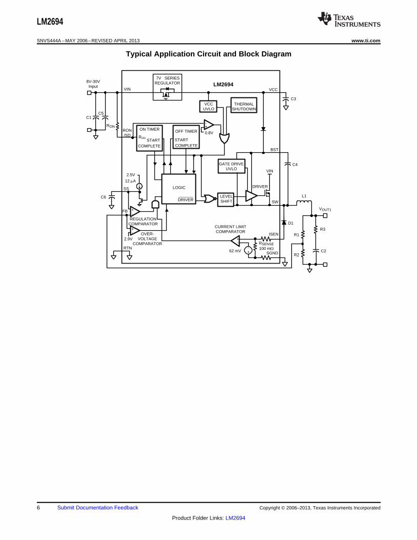
The LM2694 Step Down Switching Regulator features all the functions needed to implement a low cost, efficientbuck bias power converter capable of supplying at least 0.6A to the load. This high voltage regulator contains a30V N-Channel buck switch, is easy to implement, and is available in the TSSOP-14 and the thermally enhancedWSON-10 packages. The regulator’s operation is based on a constant on-time control scheme, where the on-time is determined by VIN. This feature allows the operating frequency to remain relatively constant with load andinput voltage variations. The feedback control requires no loop compensation resulting in very fast load transientresponse. The valley current limit detection circuit, internally set at 0.62A, holds the buck switch off until the highcurrent level subsides. This scheme protects against excessively high currents if the output is short-circuitedwhen VIN is high. The functional block diagram is shown in Typical Application Circuit and Block Diagram.
The LM2694 can be applied in numerous applications to efficiently regulate down higher voltages. Additionalfeatures include: Thermal shutdown, VCC under-voltage lockout, gate drive under-voltage lockout, and maximumduty cycle limiter.
Control Circuit Overview
The LM2694 buck DC-DC regulator employs a control scheme based on a comparator and a one-shot on-timer,with the output voltage feedback (FB) compared to an internal reference (2.5V). If the FB voltage is below thereference the buck switch is turned on for a time period determined by the input voltage and a programmingresistor (RON). Following the on-time the switch remains off for a minimum of 265 ns, and until the FB voltagefalls below the reference. The buck switch then turns on for another on-time period. Typically, during start-up, orwhen the load current increases suddenly, the off-times are at the minimum of 265 ns. Once regulation isestablished, the off-times are longer.
When in regulation, the LM2694 operates in continuous conduction mode at heavy load currents anddiscontinuous conduction mode at light load currents. In continuous conduction mode current always flowsthrough the inductor, never reaching zero during the off-time. In this mode the operating frequency remainsrelatively constant with load and line variations. The minimum load current for continuous conduction mode isone-half the inductor’s ripple current amplitude. The operating frequency is approximately:
(1)
The buck switch duty cycle is equal to:
(2)
In discontinuous conduction mode current through the inductor ramps up from zero to a peak during the on-time,then ramps back to zero before the end of the off-time. The next on-time period starts when the voltage at FBfalls below the reference - until then the inductor current remains zero, and the load current is supplied by theoutput capacitor (C2). In this mode the operating frequency is lower than in continuous conduction mode, andvaries with load current. Conversion efficiency is maintained at light loads since the switching losses reduce withthe reduction in load and frequency. The approximate discontinuous operating frequency can be calculated asfollows:
where• RL = the load resistance (3)
The output voltage is set by two external resistors (R1, R2). The regulated output voltage is calculated asfollows:
VOUT = 2.5 x (R1 + R2) / R2 (4)
Output voltage regulation is based on ripple voltage at the feedback input, requiring a minimum amount of ESRfor the output capacitor C2. The LM2694 requires a minimum of 25 mV of ripple voltage at the FB pin. In caseswhere the capacitor’s ESR is insufficient additional series resistance may be required (R3 in Typical ApplicationCircuit and Block Diagram).
Start-Up Regulator, VCC
The start-up regulator is integral to the LM2694. The input pin (VIN) can be connected directly to line voltage upto 30V, with transient capability to 33V. The VCC output regulates at 7.0V, and is current limited at 9 mA. Uponpower up, the regulator sources current into the external capacitor at VCC (C3). When the voltage on the VCCpin reaches the under-voltage lockout threshold of 5.7V, the buck switch is enabled and the Softstart pin isreleased to allow the Softstart capacitor (C6) to charge up.
The minimum input voltage is determined by the regulator’s dropout voltage, the VCC UVLO falling threshold(≊5.5V), and the frequency. When VCC falls below the falling threshold the VCC UVLO activates to shut off theoutput. If VCC is externally loaded, the minimum input voltage increases.
To reduce power dissipation in the start-up regulator, an auxiliary voltage can be diode connected to the VCC pin.Setting the auxiliary voltage to between 8V and 14V shuts off the internal regulator, reducing internal powerdissipation. The sum of the auxiliary voltage and the input voltage (VCC + VIN) cannot exceed 47V. Internally, adiode connects VCC to VIN. See Figure 10.
The feedback voltage at FB is compared to the voltage at the Softstart pin (2.5V). In normal operation (the outputvoltage is regulated), an on-time period is initiated when the voltage at FB falls below 2.5V. The buck switchstays on for the programmed on-time, causing the FB voltage to rise above 2.5V. After the on-time period, thebuck switch stays off until the FB voltage falls below 2.5V. Input bias current at the FB pin is less than 100 nAover temperature.
Over-Voltage Comparator
The voltage at FB is compared to an internal 2.9V reference. If the voltage at FB rises above 2.9V the on-timepulse is immediately terminated. This condition can occur if the input voltage or the output load changessuddenly, or if the inductor (L1) saturates. The buck switch remains off until the voltage at FB falls below 2.5V.
ON-Time Timer, and Shutdown
The on-time for the LM2694 is determined by the RON resistor and the input voltage (VIN), and is calculated from:
(5)
See Figure 6. The inverse relationship with VIN results in a nearly constant frequency as VIN is varied. To set aspecific continuous conduction mode switching frequency (FS), the RON resistor is determined from the following:
(6)
In high frequency applications the minimum value for tON is limited by the maximum duty cycle required forregulation and the minimum off-time of 265 ns, ±15%. The minimum off-time limits the maximum duty cycleachievable with a low voltage at VIN. The minimum allowed on-time to regulate the desired VOUT at the minimumVIN is determined from the following:
(7)
The LM2694 can be remotely shut down by taking the RON/SD pin below 0.8V. See Figure 11. In this mode theSS pin is internally grounded, the on-timer is disabled, and bias currents are reduced. Releasing the RON/SD pinallows normal operation to resume. The voltage at the RON/SD pin is normally between 1.5V and 3.0V,depending on VIN and the RON resistor.
Current limit detection occurs during the off-time by monitoring the recirculating current through the free-wheelingdiode (D1). Referring to Typical Application Circuit and Block Diagram, when the buck switch is turned off theinductor current flows through the load, into SGND, through the sense resistor, out of ISEN and through D1. Ifthat current exceeds 0.62A the current limit comparator output switches to delay the start of the next on-timeperiod if the voltage at FB is below 2.5V. The next on-time starts when the current out of ISEN is below 0.62Aand the voltage at FB is below 2.5V. If the overload condition persists causing the inductor current to exceed0.62A during each on-time, that is detected at the beginning of each off-time. The operating frequency is lowerdue to longer-than-normal off-times.
Figure 12 illustrates the inductor current waveform. During normal operation the load current is Io, the average ofthe ripple waveform. When the load resistance decreases the current ratchets up until the lower peak reaches0.62A. During the Current Limited portion of Figure 12, the current ramps down to 0.62A during each off-time,initiating the next on-time (assuming the voltage at FB is <2.5V). During each on-time the current ramps up anamount equal to:
ΔI = (VIN - VOUT) x tON / L1 (8)
During this time the LM2694 is in a constant current mode, with an average load current (IOCL) equal to 0.62A +ΔI/2.
Figure 12. Inductor Current - Current Limit Operation
N - Channel Buck Switch and Driver
The LM2694 integrates an N-Channel buck switch and associated floating high voltage gate driver. The peakcurrent allowed through the buck switch is 1.5A, and the maximum allowed average current is 1A. The gatedriver circuit works in conjunction with an external bootstrap capacitor and an internal high voltage diode. A 0.022µF capacitor (C4) connected between BST and SW provides the voltage to the driver during the on-time. Duringeach off-time, the SW pin is at approximately -1V, and C4 charges from VCC through the internal diode. Theminimum off-time of 265 ns ensures a minimum time each cycle to recharge the bootstrap capacitor.
The softstart feature allows the converter to gradually reach a steady state operating point, thereby reducingstart-up stresses and current surges. Upon turn-on, after VCC reaches the under-voltage threshold, an internal 12µA current source charges up the external capacitor at the SS pin to 2.5V. The ramping voltage at SS (and thenon-inverting input of the regulation comparator) ramps up the output voltage in a controlled manner.
An internal switch grounds the SS pin if VCC is below the under-voltage lockout threshold, if a thermal shutdownoccurs, or if the RON/SD pin is grounded.
Thermal Shutdown
The LM2694 should be operated so the junction temperature does not exceed 125°C. If the junction temperatureincreases, an internal Thermal Shutdown circuit, which activates (typically) at 175°C, takes the controller to a lowpower reset state by disabling the buck switch and the on-timer, and grounding the Softstart pin. This featurehelps prevent catastrophic failures from accidental device overheating. When the junction temperature reducesbelow 155°C (typical hysteresis = 20°C), the Softstart pin is released and normal operation resumes.
APPLICATIONS INFORMATION
EXTERNAL COMPONENTS
The procedure for calculating the external components is illustrated with a design example. Referring to theBlock Diagram, the circuit is to be configured for the following specifications:• VOUT = 5V• VIN = 8V to 30V• FS = 250 kHz• Minimum load current = 100 mA• Maximum load current = 600 mA• Softstart time = 5 ms.
R1 and R2: These resistors set the output voltage, and their ratio is calculated from:R1/R2 = (VOUT/2.5V) - 1 (9)
R1/R2 calculates to 1.0. The resistors should be chosen from standard value resistors in the range of 1.0 kΩ - 10kΩ. A value of 2.5 kΩ will be used for R1 and for R2.
RON, FS: RON can be chosen using Equation 6 to set the nominal frequency, or from Equation 5 if the on-time ata particular VIN is important. A higher frequency generally means a smaller inductor and capacitors (value, sizeand cost), but higher switching losses. A lower frequency means a higher efficiency, but with larger components.Generally, if PC board space is tight, a higher frequency is better. The resulting on-time and frequency have a±25% tolerance. Using Equation 6 at a VIN of 8V,
(10)
A value of 140 kΩ will be used for RON, yielding a nominal frequency of 252 kHz.
L1: The guideline for choosing the inductor value in this example is that it must keep the circuit’s operation incontinuous conduction mode at minimum load current. This is not a strict requirement since the LM2694regulates correctly when in discontinuous conduction mode, although at a lower frequency. However, to providean initial value for L1 the above guideline will be used.
1.14 x 10-10 x (140k + 1.4k)+ 95 ns x 1.25 = 3.22 Ps
IOR(max) = 120 PH x 189 kHz x 30V5V x (30V - 5V)
= 184 mAp-p
IOR(max) = L1MIN x FS(min) x VIN(max)
VOUT x (VIN(max) - VOUT)
L1 =0.2A x 189 kHz x 30V
5V x (30V - 5V)= 110 PH
L1 =IOR x FS(min) x VIN(max)
VOUT x (VIN(max) - VOUT)
L1
Cu
rren
t
0 mA
IOR
1/Fs
IPK+
IO
IPK-
LM2694
SNVS444A –MAY 2006–REVISED APRIL 2013 www.ti.com
Figure 13. Inductor Current
To keep the circuit in continuous conduction mode, the maximum allowed ripple current is twice the minimumload current, or 200 mAp-p. Using this value of ripple current, the inductor (L1) is calculated using the following:
where• FS(min) is the minimum frequency of 189 kHz (252 kHz - 25%) (11)
(12)
This provides a minimum value for L1 - the next higher standard value (150 µH) will be used. To preventsaturation, and possible destructive current levels, L1 must be rated for the peak current which occurs if thecurrent limit and maximum ripple current are reached simultaneously. The maximum ripple amplitude iscalculated by re-arranging Equation 11 using VIN(max), FS(min), and the minimum inductor value, based on themanufacturer’s tolerance. Assume, for this exercise, the inductor’s tolerance is ±20%.
(13)
(14)IPK = ILIM + IOR(max) = 0.74A + 0.18A = 0.92A
where• ILIM is the maximum specified current limit threshold (15)
At the nominal maximum load current of 0.6A, the peak inductor current is 692 mA.
C1: This capacitor limits the ripple voltage at VIN resulting from the source impedance of the supply feeding thiscircuit, and the on/off nature of the switch current into VIN. At maximum load current, when the buck switch turnson, the current into VIN steps up from zero to the lower peak of the inductor current waveform (IPK-in Figure 13),ramps up to the peak value (IPK+), then drops to zero at turn-off. The average current into VIN during this on-timeis the load current. For a worst case calculation, C1 must supply this average current during the maximum on-time. The maximum on-time is calculated at VIN = 8V using Equation 5, with a 25% tolerance added:
(16)
The voltage at VIN should not be allowed to drop below 7.5V in order to maintain VCC above its UVLO.
Normally a lower value can be used for C1 since the above calculation is a worst case calculation whichassumes the power source has a high source impedance. A quality ceramic capacitor with a low ESR should beused for C1.
C2 and R3: Since the LM2694 requires a minimum of 25 mVp-p of ripple at the FB pin for proper operation, therequired ripple at VOUT is increased by R1 and R2, and is equal to:
VRIPPLE = 25 mVp-p x (R1 + R2)/R2 = 50 mVp-p (18)
This necessary ripple voltage is created by the inductor ripple current acting on C2’s ESR + R3. First, theminimum ripple current, which occurs at minimum VIN, maximum inductor value, and maximum frequency, isdetermined.
(19)
The minimum ESR for C2 is then equal to:
(20)
If the capacitor used for C2 does not have sufficient ESR, R3 is added in series as shown in Typical ApplicationCircuit and Block Diagram. The value chosen for C2 is application dependent, and it is recommended that it beno smaller than 3.3 µF. C2 affects the ripple at VOUT, and transient response. Experimentation is usuallynecessary to determine the optimum value for C2.
C3: The capacitor at the VCC pin provides noise filtering and stability, prevents false triggering of the VCC UVLOat the buck switch on/off transitions, and limits the peak voltage at VCC when a high voltage with a short rise timeis initially applied at VIN. C3 should be no smaller than 0.1 µF, and should be a good quality, low ESR, ceramiccapacitor, physically close to the IC pins.
C4: The recommended value for C4 is 0.022 µF. A high quality ceramic capacitor with low ESR is recommendedas C4 supplies the surge current to charge the buck switch gate at each turn-on. A low ESR also ensures acomplete recharge during each off-time.
C5: This capacitor suppresses transients and ringing due to lead inductance at VIN. A low ESR, 0.1 µF ceramicchip capacitor is recommended, located physically close to the LM2694.
C6: The capacitor at the SS pin determines the soft-start time, i.e. the time for the reference voltage at theregulation comparator, and the output voltage, to reach their final value. The capacitor value is determined fromthe following:
(21)
For a 5 ms softstart time, C6 calculates to 0.024 µF.
D1: A Schottky diode is recommended. Ultra-fast recovery diodes are not recommended as the high speedtransitions at the SW pin may inadvertently affect the IC’s operation through external or internal EMI. The diodeshould be rated for the maximum VIN (30V), the maximum load current (0.6A), and the peak current which occurswhen current limit and maximum ripple current are reached simultaneously (IPK in Figure 12), previouslycalculated to be 0.92A. The diode’s forward voltage drop affects efficiency due to the power dissipated during theoff-time. The average power dissipation in D1 is calculated from:
PD1 = VF x IO x (1 - D)
where• IO is the load current, and D is the duty cycle (22)
The LM2694 requires a minimum load current of 500 µA. If the load current falls below that level, the bootstrapcapacitor (C4) may discharge during the long off-time, and the circuit will either shutdown, or cycle on and off ata low frequency. If the load current is expected to drop below 500 µA in the application, R1 and R2 should bechosen low enough in value so they provide the minimum required current at nominal VOUT.
LOW OUTPUT RIPPLE CONFIGURATIONS
For applications where low output voltage ripple is required the output can be taken directly from the low ESRoutput capacitor (C2) as shown in Figure 17. However, R3 slightly degrades the load regulation. The specificcomponent values, and the application determine if this is suitable.
Figure 17. Low Ripple Output
Where the circuit of Figure 17 is not suitable for reducing output ripple, the circuits of Figure 18 or Figure 19 canbe used.
Figure 18. Low Output Ripple Using a Feedforward Capacitor
In Figure 18, Cff is added across R1 to AC-couple the ripple at VOUT directly to the FB pin. This allows the rippleat VOUT to be reduced, in some cases considerably, by reducing R3. In the circuit of Figure 14, the ripple at VOUTranged from 50 mVp-p at VIN = 8V to 100 mVp-p at VIN = 30V. By adding a 2700 pF capacitor at Cff andreducing R3 to 0.75Ω, the VOUT ripple is reduced by 50%.
Figure 19. Minimum Output Ripple Using Ripple Injection
To reduce VOUT ripple further, the circuit of Figure 19 can be used. R3 has been removed, and the output rippleamplitude is determined by C2’s ESR and the inductor ripple current. RA and CA are chosen to generate a 40-50mVp-p sawtooth at their junction, and that voltage is AC-coupled to the FB pin via CB. In selecting RA and CA,VOUT is considered a virtual ground as the SW pin switches between VIN and -1V. Since the on-time at SW variesinversely with VIN, the waveform amplitude at the RA/CA junction is relatively constant. Typical values for theadditional components are RA = 110k, CA = 2700 pF, and CB = 0.01 µF.
The LM2694 regulation, over-voltage, and current limit comparators are very fast, and will respond to shortduration noise pulses. Layout considerations are therefore critical for optimum performance. The layout must beas neat and compact as possible, and all the components must be as close as possible to their associated pins.The two major current loops have currents which switch very fast, and so the loops should be as small aspossible to minimize conducted and radiated EMI. The first loop is that formed by C1, through the VIN to SWpins, L1, C2, and back to C1. The second loop is that formed by D1, L1, C2, and the SGND and ISEN pins. Theground connection from C2 to C1 should be as short and direct as possible, preferably without going throughvias. Directly connect the SGND and RTN pin to each other, and they should be connected as directly aspossible to the C1/C2 ground line without going through vias. The power dissipation within the IC can beapproximated by determining the total conversion loss (PIN - POUT), and then subtracting the power losses in thefree-wheeling diode and the inductor. The power loss in the diode is approximately:
PD1 = IO x VF x (1-D)
where• Io is the load current• VF is the diode’s forward voltage drop• D is the duty cycle (23)
The power loss in the inductor is approximately:PL1 = IO
2 x RL x 1.1
where• RL is the inductor’s DC resistance• 1.1 factor is an approximation for the AC losses (24)
If it is expected that the internal dissipation of the LM2694 will produce high junction temperatures during normaloperation, good use of the PC board’s ground plane can help considerably to dissipate heat. The exposed padon the WSON package bottom should be soldered to a ground plane, and that plane should both extend frombeneath the IC, and be connected to exposed ground plane on the board’s other side using as many vias aspossible. The exposed pad is internally connected to the IC substrate. The use of wide PC board traces at thepins, where possible, can help conduct heat away from the IC. The four No Connect pins on the TSSOP packageare not electrically connected to any part of the IC, and may be connected to ground plane to help dissipate heatfrom the package. Judicious positioning of the PC board within the end product, along with the use of anyavailable air flow (forced or natural convection) can help reduce the junction temperature.
Changes from Original (April 2013) to Revision A Page
• Changed layout of National Data Sheet to TI format .......................................................................................................... 16
LM2694MT/NOPB ACTIVE TSSOP PW 14 94 Green (RoHS& no Sb/Br)
CU SN Level-1-260C-UNLIM L2694MT
LM2694MTX NRND TSSOP PW 14 TBD Call TI Call TI L2694MT
LM2694MTX/NOPB ACTIVE TSSOP PW 14 2500 Green (RoHS& no Sb/Br)
CU SN Level-1-260C-UNLIM L2694MT
LM2694SD/NOPB ACTIVE WSON DSC 10 1000 Green (RoHS& no Sb/Br)
CU SN Level-1-260C-UNLIM -40 to 125 L2694
(1) The marketing status values are defined as follows:ACTIVE: Product device recommended for new designs.LIFEBUY: TI has announced that the device will be discontinued, and a lifetime-buy period is in effect.NRND: Not recommended for new designs. Device is in production to support existing customers, but TI does not recommend using this part in a new design.PREVIEW: Device has been announced but is not in production. Samples may or may not be available.OBSOLETE: TI has discontinued the production of the device.
(2) Eco Plan - The planned eco-friendly classification: Pb-Free (RoHS), Pb-Free (RoHS Exempt), or Green (RoHS & no Sb/Br) - please check http://www.ti.com/productcontent for the latest availabilityinformation and additional product content details.TBD: The Pb-Free/Green conversion plan has not been defined.Pb-Free (RoHS): TI's terms "Lead-Free" or "Pb-Free" mean semiconductor products that are compatible with the current RoHS requirements for all 6 substances, including the requirement thatlead not exceed 0.1% by weight in homogeneous materials. Where designed to be soldered at high temperatures, TI Pb-Free products are suitable for use in specified lead-free processes.Pb-Free (RoHS Exempt): This component has a RoHS exemption for either 1) lead-based flip-chip solder bumps used between the die and package, or 2) lead-based die adhesive used betweenthe die and leadframe. The component is otherwise considered Pb-Free (RoHS compatible) as defined above.Green (RoHS & no Sb/Br): TI defines "Green" to mean Pb-Free (RoHS compatible), and free of Bromine (Br) and Antimony (Sb) based flame retardants (Br or Sb do not exceed 0.1% by weightin homogeneous material)
(3) MSL, Peak Temp. - The Moisture Sensitivity Level rating according to the JEDEC industry standard classifications, and peak solder temperature.
(4) There may be additional marking, which relates to the logo, the lot trace code information, or the environmental category on the device.
(5) Multiple Device Markings will be inside parentheses. Only one Device Marking contained in parentheses and separated by a "~" will appear on a device. If a line is indented then it is a continuationof the previous line and the two combined represent the entire Device Marking for that device.
(6) Lead/Ball Finish - Orderable Devices may have multiple material finish options. Finish options are separated by a vertical ruled line. Lead/Ball Finish values may wrap to two lines if the finishvalue exceeds the maximum column width.
Important Information and Disclaimer:The information provided on this page represents TI's knowledge and belief as of the date that it is provided. TI bases its knowledge and belief on informationprovided by third parties, and makes no representation or warranty as to the accuracy of such information. Efforts are underway to better integrate information from third parties. TI has taken andcontinues to take reasonable steps to provide representative and accurate information but may not have conducted destructive testing or chemical analysis on incoming materials and chemicals.TI and TI suppliers consider certain information to be proprietary, and thus CAS numbers and other limited information may not be available for release.
In no event shall TI's liability arising out of such information exceed the total purchase price of the TI part(s) at issue in this document sold by TI to Customer on an annual basis.
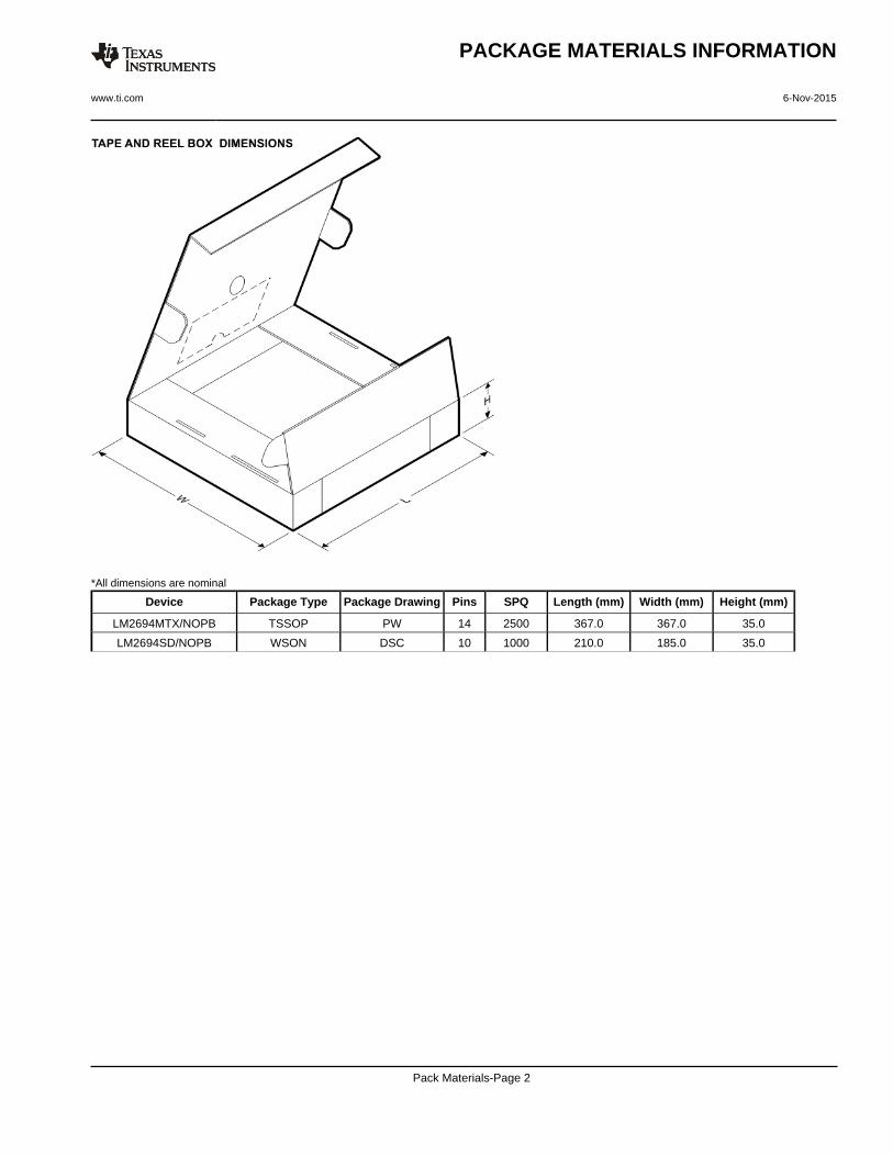
WSON - 0.8 mm max heightDSC0010BPLASTIC SMALL OUTLINE - NO LEAD
4214926/A 07/2014
PIN 1 INDEX AREA
0.08SEATING PLANE
(OPTIONAL)PIN 1 ID
1
6
10
5
0.1 C A B0.05 C
NOTES: 1. All linear dimensions are in millimeters. Any dimensions in parenthesis are for reference only. Dimensioning and tolerancing per ASME Y14.5M.2. This drawing is subject to change without notice.3. The package thermal pad must be soldered to the printed circuit board for thermal and mechanical performance.
0.08
0.1 C A B0.05 C
SCALE 4.000
www.ti.com
EXAMPLE BOARD LAYOUT
0.07 MINALL AROUND
0.07 MAXALL AROUND
(1.2)
(2)
10X (0.65)
10X (0.25)
(0.35) TYP
(0.75) TYP
(2.75)
( ) TYPVIA
0.2
8X (0.5)
WSON - 0.8 mm max heightDSC0010BPLASTIC SMALL OUTLINE - NO LEAD
4214926/A 07/2014
SYMM
SYMM
LAND PATTERN EXAMPLESCALE:20X
1
5 6
10
NOTES: (continued) 4. This package is designed to be soldered to a thermal pad on the board. For more information, see Texas Instruments literature number SLUA271 (www.ti.com/lit/slua271).
SOLDER MASKOPENING
METALUNDERSOLDER MASK
SOLDER MASKDEFINED
METALSOLDER MASKOPENING
SOLDER MASK DETAILS
NON SOLDER MASKDEFINED
(PREFERRED)
www.ti.com
EXAMPLE STENCIL DESIGN
(1.13)
(0.89)
10X (0.65)
10X (0.25)
8X (0.5)
(2.75)
(0.55)
WSON - 0.8 mm max heightDSC0010BPLASTIC SMALL OUTLINE - NO LEAD
4214926/A 07/2014
NOTES: (continued) 5. Laser cutting apertures with trapezoidal walls and rounded corners may offer better paste release. IPC-7525 may have alternate design recommendations.
SYMM
SYMM
METALTYP
SOLDER PASTE EXAMPLEBASED ON 0.125 mm THICK STENCIL
EXPOSED PAD
84% PRINTED SOLDER COVERAGE BY AREASCALE:25X
IMPORTANT NOTICE
Texas Instruments Incorporated and its subsidiaries (TI) reserve the right to make corrections, enhancements, improvements and otherchanges to its semiconductor products and services per JESD46, latest issue, and to discontinue any product or service per JESD48, latestissue. Buyers should obtain the latest relevant information before placing orders and should verify that such information is current andcomplete. All semiconductor products (also referred to herein as “components”) are sold subject to TI’s terms and conditions of salesupplied at the time of order acknowledgment.TI warrants performance of its components to the specifications applicable at the time of sale, in accordance with the warranty in TI’s termsand conditions of sale of semiconductor products. Testing and other quality control techniques are used to the extent TI deems necessaryto support this warranty. Except where mandated by applicable law, testing of all parameters of each component is not necessarilyperformed.TI assumes no liability for applications assistance or the design of Buyers’ products. Buyers are responsible for their products andapplications using TI components. To minimize the risks associated with Buyers’ products and applications, Buyers should provideadequate design and operating safeguards.TI does not warrant or represent that any license, either express or implied, is granted under any patent right, copyright, mask work right, orother intellectual property right relating to any combination, machine, or process in which TI components or services are used. Informationpublished by TI regarding third-party products or services does not constitute a license to use such products or services or a warranty orendorsement thereof. Use of such information may require a license from a third party under the patents or other intellectual property of thethird party, or a license from TI under the patents or other intellectual property of TI.Reproduction of significant portions of TI information in TI data books or data sheets is permissible only if reproduction is without alterationand is accompanied by all associated warranties, conditions, limitations, and notices. TI is not responsible or liable for such altereddocumentation. Information of third parties may be subject to additional restrictions.Resale of TI components or services with statements different from or beyond the parameters stated by TI for that component or servicevoids all express and any implied warranties for the associated TI component or service and is an unfair and deceptive business practice.TI is not responsible or liable for any such statements.Buyer acknowledges and agrees that it is solely responsible for compliance with all legal, regulatory and safety-related requirementsconcerning its products, and any use of TI components in its applications, notwithstanding any applications-related information or supportthat may be provided by TI. Buyer represents and agrees that it has all the necessary expertise to create and implement safeguards whichanticipate dangerous consequences of failures, monitor failures and their consequences, lessen the likelihood of failures that might causeharm and take appropriate remedial actions. Buyer will fully indemnify TI and its representatives against any damages arising out of the useof any TI components in safety-critical applications.In some cases, TI components may be promoted specifically to facilitate safety-related applications. With such components, TI’s goal is tohelp enable customers to design and create their own end-product solutions that meet applicable functional safety standards andrequirements. Nonetheless, such components are subject to these terms.No TI components are authorized for use in FDA Class III (or similar life-critical medical equipment) unless authorized officers of the partieshave executed a special agreement specifically governing such use.Only those TI components which TI has specifically designated as military grade or “enhanced plastic” are designed and intended for use inmilitary/aerospace applications or environments. Buyer acknowledges and agrees that any military or aerospace use of TI componentswhich have not been so designated is solely at the Buyer's risk, and that Buyer is solely responsible for compliance with all legal andregulatory requirements in connection with such use.TI has specifically designated certain components as meeting ISO/TS16949 requirements, mainly for automotive use. In any case of use ofnon-designated products, TI will not be responsible for any failure to meet ISO/TS16949.
Products ApplicationsAudio www.ti.com/audio Automotive and Transportation www.ti.com/automotiveAmplifiers amplifier.ti.com Communications and Telecom www.ti.com/communicationsData Converters dataconverter.ti.com Computers and Peripherals www.ti.com/computersDLP® Products www.dlp.com Consumer Electronics www.ti.com/consumer-appsDSP dsp.ti.com Energy and Lighting www.ti.com/energyClocks and Timers www.ti.com/clocks Industrial www.ti.com/industrialInterface interface.ti.com Medical www.ti.com/medicalLogic logic.ti.com Security www.ti.com/securityPower Mgmt power.ti.com Space, Avionics and Defense www.ti.com/space-avionics-defenseMicrocontrollers microcontroller.ti.com Video and Imaging www.ti.com/videoRFID www.ti-rfid.comOMAP Applications Processors www.ti.com/omap TI E2E Community e2e.ti.comWireless Connectivity www.ti.com/wirelessconnectivity