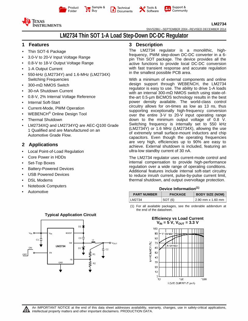
LM2734 VIN VIN EN BOOST SW FB GND VOUT C3 L1 C1 C2 R1 R2 D1 D2 ON OFF Product Folder Sample & Buy Technical Documents Tools & Software Support & Community LM2734 SNVS288J – SEPTEMBER 2004 – REVISED DECEMBER 2014 LM2734 Thin SOT 1-A Load Step-Down DC-DC Regulator 1 Features 3 Description The LM2734 regulator is a monolithic, high- 1• Thin SOT-6 Package frequency, PWM step-down DC-DC converter in a 6- • 3.0-V to 20-V Input Voltage Range pin Thin SOT package. The device provides all the • 0.8-V to 18-V Output Voltage Range active functions to provide local DC-DC conversion with fast transient response and accurate regulation • 1-A Output Current in the smallest possible PCB area. • 550-kHz (LM2734Y) and 1.6-MHz (LM2734X) Switching Frequencies With a minimum of external components and online design support through WEBENCH, the LM2734 • 300-mΩ NMOS Switch regulator is easy to use. The ability to drive 1-A loads • 30-nA Shutdown Current with an internal 300-mΩ NMOS switch using state-of- • 0.8-V, 2% Internal Voltage Reference the-art 0.5-μm BiCMOS technology results in the best power density available. The world-class control • Internal Soft-Start circuitry allows for on-times as low as 13 ns, thus • Current-Mode, PWM Operation supporting exceptionally high-frequency conversion • WEBENCH ® Online Design Tool over the entire 3-V to 20-V input operating range down to the minimum output voltage of 0.8 V. • Thermal Shutdown Switching frequency is internally set to 550 kHz • LM2734XQ and LM2734YQ are AEC-Q100 Grade (LM2734Y) or 1.6 MHz (LM2734X), allowing the use 1 Qualified and are Manufactured on an of extremely small surface-mount inductors and chip Automotive Grade Flow. capacitors. Even though the operating frequencies are very high, efficiencies up to 90% are easy to 2 Applications achieve. External shutdown is included, featuring an ultra-low standby current of 30 nA. • Local Point-of-Load Regulation • Core Power in HDDs The LM2734 regulator uses current-mode control and internal compensation to provide high-performance • Set-Top Boxes regulation over a wide range of operating conditions. • Battery-Powered Devices Additional features include internal soft-start circuitry • USB Powered Devices to reduce inrush current, pulse-by-pulse current limit, thermal shutdown, and output overvoltage protection. • DSL Modems • Notebook Computers Device Information (1) • Automotive PART NUMBER PACKAGE BODY SIZE (NOM) LM2734 SOT (6) 2.90 mm x 1.60 mm (1) For all available packages, see the orderable addendum at the end of the datasheet. Typical Application Circuit Efficiency vs Load Current V IN = 5 V, V OUT = 3.3 V 1 An IMPORTANT NOTICE at the end of this data sheet addresses availability, warranty, changes, use in safety-critical applications, intellectual property matters and other important disclaimers. PRODUCTION DATA.
Transcript
LM2734
VIN VIN
EN
BOOST
SW
FB
GND
VOUT
C3 L1C1
C2
R1
R2
D1
D2
ON
OFF
Product
Folder
Sample &Buy
Technical
Documents
Tools &
Software
Support &Community
LM2734SNVS288J –SEPTEMBER 2004–REVISED DECEMBER 2014
LM2734 Thin SOT 1-A Load Step-Down DC-DC Regulator1 Features 3 Description
The LM2734 regulator is a monolithic, high-1• Thin SOT-6 Package
frequency, PWM step-down DC-DC converter in a 6-• 3.0-V to 20-V Input Voltage Range pin Thin SOT package. The device provides all the• 0.8-V to 18-V Output Voltage Range active functions to provide local DC-DC conversion
with fast transient response and accurate regulation• 1-A Output Currentin the smallest possible PCB area.• 550-kHz (LM2734Y) and 1.6-MHz (LM2734X)
Switching Frequencies With a minimum of external components and onlinedesign support through WEBENCH, the LM2734• 300-mΩ NMOS Switchregulator is easy to use. The ability to drive 1-A loads• 30-nA Shutdown Current with an internal 300-mΩ NMOS switch using state-of-
• 0.8-V, 2% Internal Voltage Reference the-art 0.5-µm BiCMOS technology results in the bestpower density available. The world-class control• Internal Soft-Startcircuitry allows for on-times as low as 13 ns, thus• Current-Mode, PWM Operation supporting exceptionally high-frequency conversion
• WEBENCH® Online Design Tool over the entire 3-V to 20-V input operating rangedown to the minimum output voltage of 0.8 V.• Thermal ShutdownSwitching frequency is internally set to 550 kHz• LM2734XQ and LM2734YQ are AEC-Q100 Grade(LM2734Y) or 1.6 MHz (LM2734X), allowing the use1 Qualified and are Manufactured on an of extremely small surface-mount inductors and chipAutomotive Grade Flow. capacitors. Even though the operating frequenciesare very high, efficiencies up to 90% are easy to2 Applications achieve. External shutdown is included, featuring anultra-low standby current of 30 nA.• Local Point-of-Load Regulation
• Core Power in HDDs The LM2734 regulator uses current-mode control andinternal compensation to provide high-performance• Set-Top Boxesregulation over a wide range of operating conditions.• Battery-Powered Devices Additional features include internal soft-start circuitry
• USB Powered Devices to reduce inrush current, pulse-by-pulse current limit,thermal shutdown, and output overvoltage protection.• DSL Modems
• Notebook ComputersDevice Information(1)
• AutomotivePART NUMBER PACKAGE BODY SIZE (NOM)
LM2734 SOT (6) 2.90 mm x 1.60 mm
(1) For all available packages, see the orderable addendum atthe end of the datasheet.
Typical Application CircuitEfficiency vs Load Current
VIN = 5 V, VOUT = 3.3 V
1
An IMPORTANT NOTICE at the end of this data sheet addresses availability, warranty, changes, use in safety-critical applications,intellectual property matters and other important disclaimers. PRODUCTION DATA.
LM2734www.ti.com SNVS288J –SEPTEMBER 2004–REVISED DECEMBER 2014
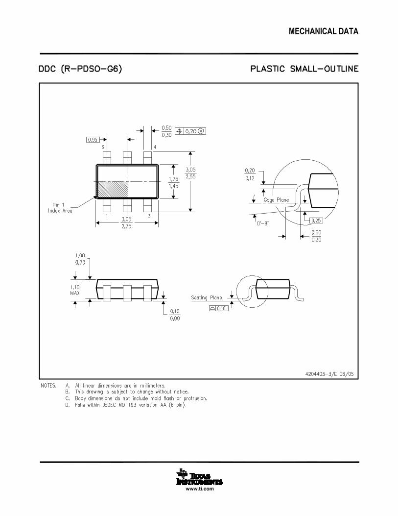
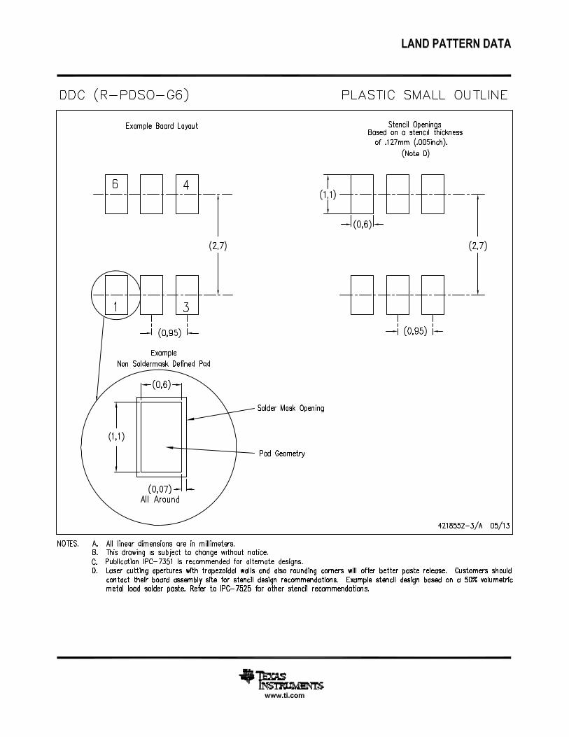
5 Pin Configuration and Functions
See Package Number DDC (R-PDSO-G6)6-Lead SOT
Top View
Pin FunctionsPIN
I/O DESCRIPTIONNAME NO.
Boost voltage that drives the internal NMOS control switch. A bootstrap capacitor isBOOST 1 I connected between the BOOST and SW pins.Signal and Power ground pin. Place the bottom resistor of the feedback network as close asGND 2 GND possible to this pin for accurate regulation.
FB 3 I Feedback pin. Connect FB to the external resistor divider to set output voltage.Enable control input. Logic high enables operation. Do not allow this pin to float or be greaterEN 4 I than VIN + 0.3 V.
VIN 5 I Input supply voltage. Connect a bypass capacitor to this pin.SW 6 O Output switch. Connects to the inductor, catch diode, and bootstrap capacitor.
LM2734SNVS288J –SEPTEMBER 2004–REVISED DECEMBER 2014 www.ti.com
6 Specifications
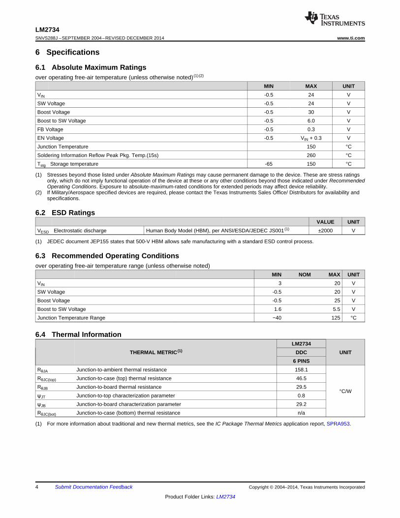
6.1 Absolute Maximum Ratingsover operating free-air temperature (unless otherwise noted) (1) (2)
MIN MAX UNITVIN -0.5 24 VSW Voltage -0.5 24 VBoost Voltage -0.5 30 VBoost to SW Voltage -0.5 6.0 VFB Voltage -0.5 0.3 VEN Voltage -0.5 VIN + 0.3 VJunction Temperature 150 °CSoldering Information Reflow Peak Pkg. Temp.(15s) 260 °CTstg Storage temperature -65 150 °C
(1) Stresses beyond those listed under Absolute Maximum Ratings may cause permanent damage to the device. These are stress ratingsonly, which do not imply functional operation of the device at these or any other conditions beyond those indicated under RecommendedOperating Conditions. Exposure to absolute-maximum-rated conditions for extended periods may affect device reliability.
(2) If Military/Aerospace specified devices are required, please contact the Texas Instruments Sales Office/ Distributors for availability andspecifications.
6.2 ESD RatingsVALUE UNIT
VESD Electrostatic discharge Human Body Model (HBM), per ANSI/ESDA/JEDEC JS001 (1) ±2000 V
(1) JEDEC document JEP155 states that 500-V HBM allows safe manufacturing with a standard ESD control process.
6.3 Recommended Operating Conditionsover operating free-air temperature range (unless otherwise noted)
MIN NOM MAX UNITVIN 3 20 VSW Voltage -0.5 20 VBoost Voltage -0.5 25 VBoost to SW Voltage 1.6 5.5 VJunction Temperature Range −40 125 °C
LM2734SNVS288J –SEPTEMBER 2004–REVISED DECEMBER 2014 www.ti.com
7 Detailed Description
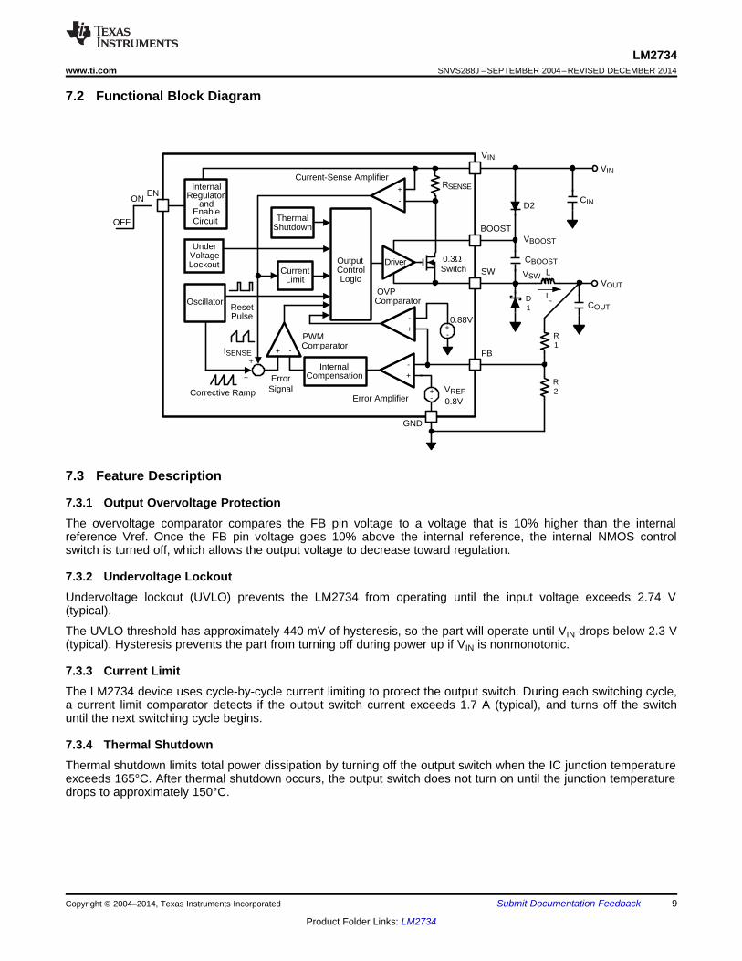
7.1 OverviewThe LM2734 device is a constant frequency PWM buck regulator IC that delivers a 1-A load current. Theregulator has a preset switching frequency of either 550 kHz (LM2734Y) or 1.6 MHz (LM2734X). These highfrequencies allow the LM2734 device to operate with small surface-mount capacitors and inductors, resulting inDC-DC converters that require a minimum amount of board space. The LM2734 device is internallycompensated, so it is simple to use, and requires few external components. The LM2734 device uses current-mode control to regulate the output voltage.
The following operating description of the LM2734 device will refer to the Simplified Block Diagram () and to thewaveforms in Figure 12. The LM2734 device supplies a regulated output voltage by switching the internal NMOScontrol switch at constant frequency and variable duty cycle. A switching cycle begins at the falling edge of thereset pulse generated by the internal oscillator. When this pulse goes low, the output control logic turns on theinternal NMOS control switch. During this on-time, the SW pin voltage (VSW) swings up to approximately VIN, andthe inductor current (IL) increases with a linear slope. IL is measured by the current-sense amplifier, whichgenerates an output proportional to the switch current. The sense signal is summed with the regulator’scorrective ramp and compared to the error amplifier’s output, which is proportional to the difference between thefeedback voltage and VREF. When the PWM comparator output goes high, the output switch turns off until thenext switching cycle begins. During the switch off-time, inductor current discharges through Schottky diode D1,which forces the SW pin to swing below ground by the forward voltage (VD) of the catch diode. The regulatorloop adjusts the duty cycle (D) to maintain a constant output voltage.
Figure 12. LM2734 Waveforms of SW Pin Voltage and Inductor Current
LM2734www.ti.com SNVS288J –SEPTEMBER 2004–REVISED DECEMBER 2014
7.2 Functional Block Diagram
7.3 Feature Description
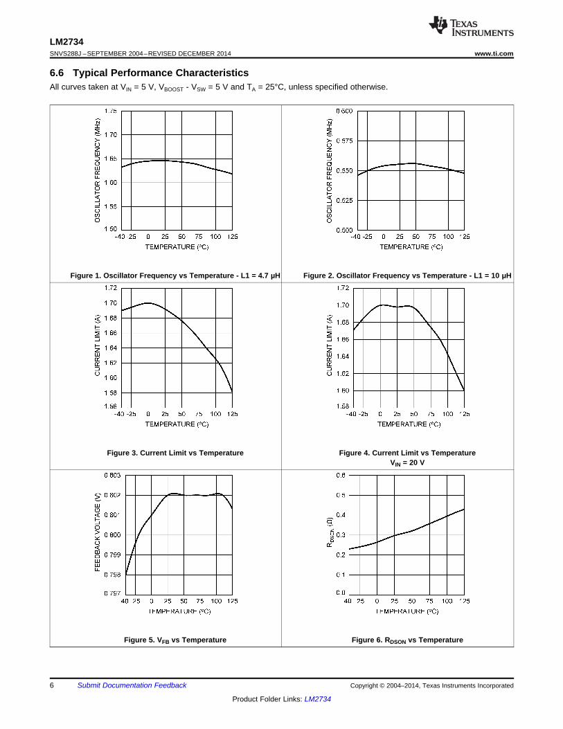
7.3.1 Output Overvoltage ProtectionThe overvoltage comparator compares the FB pin voltage to a voltage that is 10% higher than the internalreference Vref. Once the FB pin voltage goes 10% above the internal reference, the internal NMOS controlswitch is turned off, which allows the output voltage to decrease toward regulation.
7.3.2 Undervoltage LockoutUndervoltage lockout (UVLO) prevents the LM2734 from operating until the input voltage exceeds 2.74 V(typical).
The UVLO threshold has approximately 440 mV of hysteresis, so the part will operate until VIN drops below 2.3 V(typical). Hysteresis prevents the part from turning off during power up if VIN is nonmonotonic.
7.3.3 Current LimitThe LM2734 device uses cycle-by-cycle current limiting to protect the output switch. During each switching cycle,a current limit comparator detects if the output switch current exceeds 1.7 A (typical), and turns off the switchuntil the next switching cycle begins.
7.3.4 Thermal ShutdownThermal shutdown limits total power dissipation by turning off the output switch when the IC junction temperatureexceeds 165°C. After thermal shutdown occurs, the output switch does not turn on until the junction temperaturedrops to approximately 150°C.
LM2734SNVS288J –SEPTEMBER 2004–REVISED DECEMBER 2014 www.ti.com
7.4 Device Functional Modes
7.4.1 Enable Pin / Shutdown ModeThe LM2734 device has a shutdown mode that is controlled by the enable pin (EN). When a logic low voltage isapplied to EN, the part is in shutdown mode and its quiescent current drops to typically 30 nA. Switch leakageadds another 40 nA from the input supply. The voltage at this pin should never exceed VIN + 0.3 V.
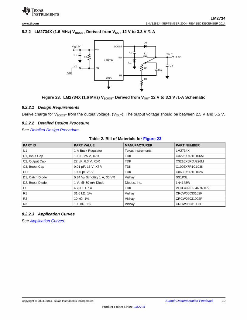
7.4.2 Soft-StartThis function forces VOUT to increase at a controlled rate during start up. During soft-start, the error amplifier’sreference voltage ramps from 0 V to its nominal value of 0.8 V in approximately 200 µs. This forces the regulatoroutput to ramp up in a more linear and controlled fashion, which helps reduce inrush current. Under somecircumstances at start-up, an output voltage overshoot may still be observed. This may be due to a large outputload applied during start up. Large amounts of output external capacitance can also increase output voltageovershoot. A simple solution is to add a feed forward capacitor with a value between 470 pf and 1000 pf acrossthe top feedback resistor (R1). See Figure 23 for further detail.
LM2734www.ti.com SNVS288J –SEPTEMBER 2004–REVISED DECEMBER 2014
8 Application and Implementation
NOTEInformation in the following applications sections is not part of the TI componentspecification, and TI does not warrant its accuracy or completeness. TI’s customers areresponsible for determining suitability of components for their purposes. Customers shouldvalidate and test their design implementation to confirm system functionality.
8.1 Application Information
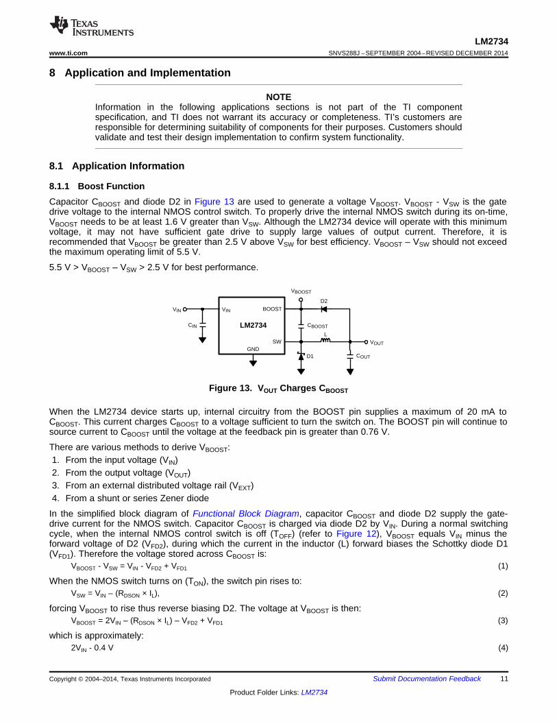
8.1.1 Boost FunctionCapacitor CBOOST and diode D2 in Figure 13 are used to generate a voltage VBOOST. VBOOST - VSW is the gatedrive voltage to the internal NMOS control switch. To properly drive the internal NMOS switch during its on-time,VBOOST needs to be at least 1.6 V greater than VSW. Although the LM2734 device will operate with this minimumvoltage, it may not have sufficient gate drive to supply large values of output current. Therefore, it isrecommended that VBOOST be greater than 2.5 V above VSW for best efficiency. VBOOST – VSW should not exceedthe maximum operating limit of 5.5 V.
5.5 V > VBOOST – VSW > 2.5 V for best performance.
Figure 13. VOUT Charges CBOOST
When the LM2734 device starts up, internal circuitry from the BOOST pin supplies a maximum of 20 mA toCBOOST. This current charges CBOOST to a voltage sufficient to turn the switch on. The BOOST pin will continue tosource current to CBOOST until the voltage at the feedback pin is greater than 0.76 V.
There are various methods to derive VBOOST:1. From the input voltage (VIN)2. From the output voltage (VOUT)3. From an external distributed voltage rail (VEXT)4. From a shunt or series Zener diode
In the simplified block diagram of Functional Block Diagram, capacitor CBOOST and diode D2 supply the gate-drive current for the NMOS switch. Capacitor CBOOST is charged via diode D2 by VIN. During a normal switchingcycle, when the internal NMOS control switch is off (TOFF) (refer to Figure 12), VBOOST equals VIN minus theforward voltage of D2 (VFD2), during which the current in the inductor (L) forward biases the Schottky diode D1(VFD1). Therefore the voltage stored across CBOOST is:
VBOOST - VSW = VIN - VFD2 + VFD1 (1)
When the NMOS switch turns on (TON), the switch pin rises to:VSW = VIN – (RDSON × IL), (2)
forcing VBOOST to rise thus reverse biasing D2. The voltage at VBOOST is then:VBOOST = 2VIN – (RDSON × IL) – VFD2 + VFD1 (3)
LM2734SNVS288J –SEPTEMBER 2004–REVISED DECEMBER 2014 www.ti.com
Application Information (continued)for many applications. Thus the gate-drive voltage of the NMOS switch is approximately:
VIN - 0.2 V (5)
An alternate method for charging CBOOST is to connect D2 to the output as shown in Figure 13. The outputvoltage should be from 2.5 V and 5.5 V, so that proper gate voltage will be applied to the internal switch. In thiscircuit, CBOOST provides a gate drive voltage that is slightly less than VOUT.
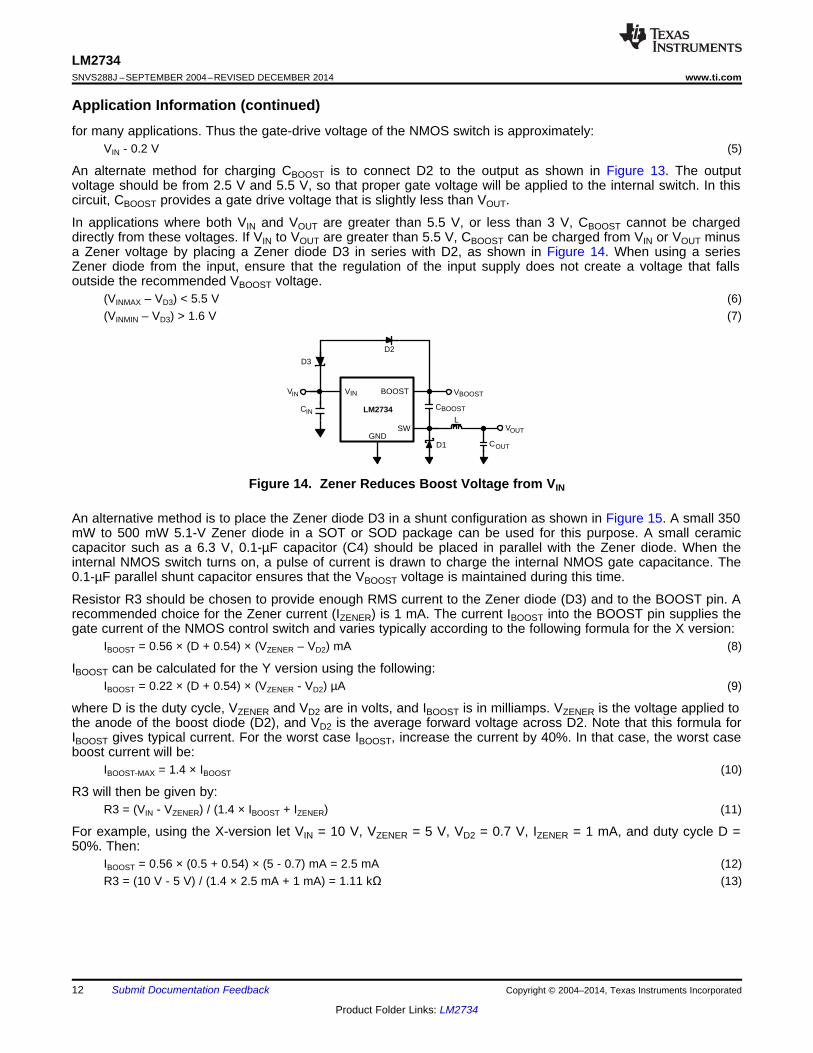
In applications where both VIN and VOUT are greater than 5.5 V, or less than 3 V, CBOOST cannot be chargeddirectly from these voltages. If VIN to VOUT are greater than 5.5 V, CBOOST can be charged from VIN or VOUT minusa Zener voltage by placing a Zener diode D3 in series with D2, as shown in Figure 14. When using a seriesZener diode from the input, ensure that the regulation of the input supply does not create a voltage that fallsoutside the recommended VBOOST voltage.
(VINMAX – VD3) < 5.5 V (6)(VINMIN – VD3) > 1.6 V (7)
Figure 14. Zener Reduces Boost Voltage from VIN
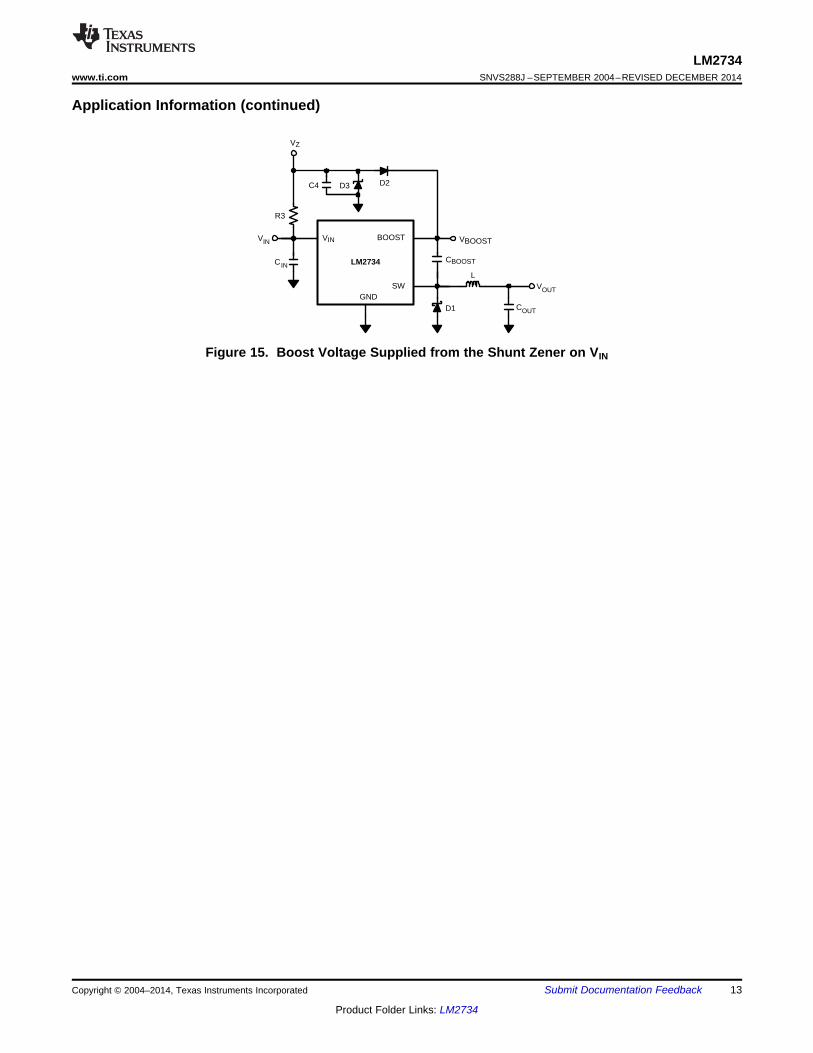
An alternative method is to place the Zener diode D3 in a shunt configuration as shown in Figure 15. A small 350mW to 500 mW 5.1-V Zener diode in a SOT or SOD package can be used for this purpose. A small ceramiccapacitor such as a 6.3 V, 0.1-µF capacitor (C4) should be placed in parallel with the Zener diode. When theinternal NMOS switch turns on, a pulse of current is drawn to charge the internal NMOS gate capacitance. The0.1-µF parallel shunt capacitor ensures that the VBOOST voltage is maintained during this time.
Resistor R3 should be chosen to provide enough RMS current to the Zener diode (D3) and to the BOOST pin. Arecommended choice for the Zener current (IZENER) is 1 mA. The current IBOOST into the BOOST pin supplies thegate current of the NMOS control switch and varies typically according to the following formula for the X version:
IBOOST can be calculated for the Y version using the following:IBOOST = 0.22 × (D + 0.54) × (VZENER - VD2) µA (9)
where D is the duty cycle, VZENER and VD2 are in volts, and IBOOST is in milliamps. VZENER is the voltage applied tothe anode of the boost diode (D2), and VD2 is the average forward voltage across D2. Note that this formula forIBOOST gives typical current. For the worst case IBOOST, increase the current by 40%. In that case, the worst caseboost current will be:
IBOOST-MAX = 1.4 × IBOOST (10)
R3 will then be given by:R3 = (VIN - VZENER) / (1.4 × IBOOST + IZENER) (11)
For example, using the X-version let VIN = 10 V, VZENER = 5 V, VD2 = 0.7 V, IZENER = 1 mA, and duty cycle D =50%. Then:
IBOOST = 0.56 × (0.5 + 0.54) × (5 - 0.7) mA = 2.5 mA (12)R3 = (10 V - 5 V) / (1.4 × 2.5 mA + 1 mA) = 1.11 kΩ (13)
LM2734SNVS288J –SEPTEMBER 2004–REVISED DECEMBER 2014 www.ti.com
8.2 Typical Applications
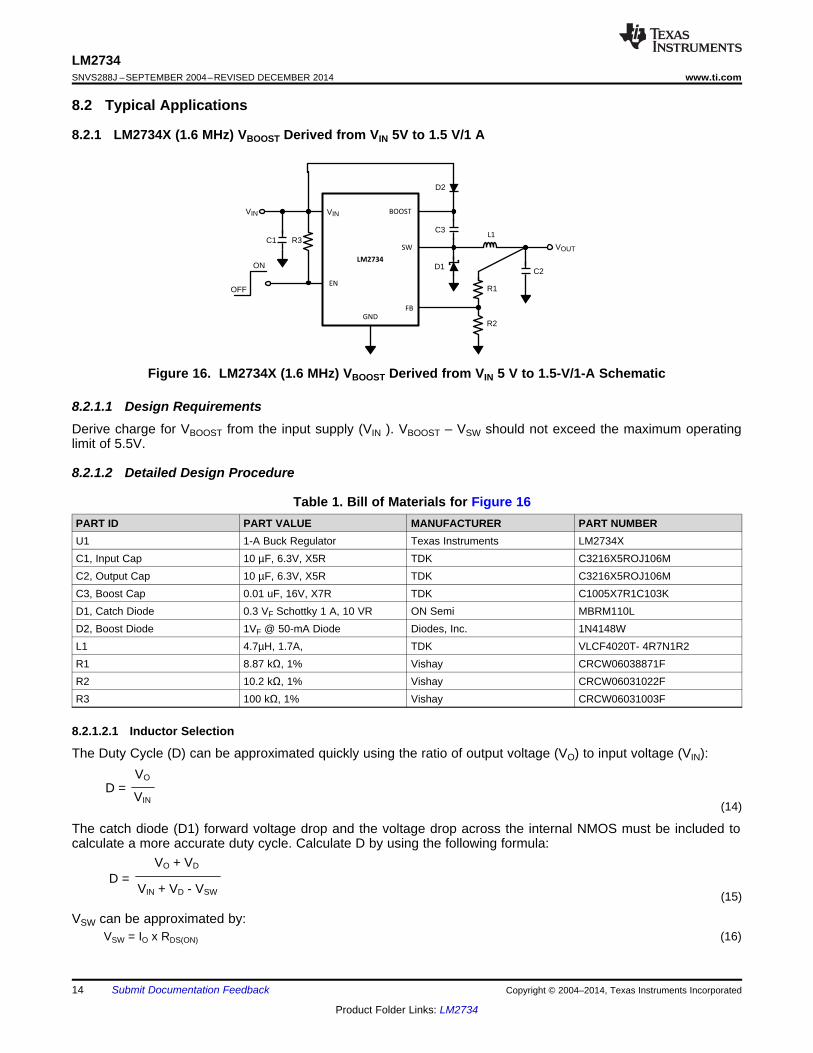
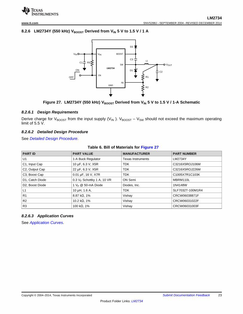
8.2.1 LM2734X (1.6 MHz) VBOOST Derived from VIN 5V to 1.5 V/1 A
Figure 16. LM2734X (1.6 MHz) VBOOST Derived from VIN 5 V to 1.5-V/1-A Schematic
8.2.1.1 Design RequirementsDerive charge for VBOOST from the input supply (VIN ). VBOOST – VSW should not exceed the maximum operatinglimit of 5.5V.
8.2.1.2 Detailed Design Procedure
Table 1. Bill of Materials for Figure 16PART ID PART VALUE MANUFACTURER PART NUMBERU1 1-A Buck Regulator Texas Instruments LM2734XC1, Input Cap 10 µF, 6.3V, X5R TDK C3216X5ROJ106MC2, Output Cap 10 µF, 6.3V, X5R TDK C3216X5ROJ106MC3, Boost Cap 0.01 uF, 16V, X7R TDK C1005X7R1C103KD1, Catch Diode 0.3 VF Schottky 1 A, 10 VR ON Semi MBRM110LD2, Boost Diode 1VF @ 50-mA Diode Diodes, Inc. 1N4148WL1 4.7µH, 1.7A, TDK VLCF4020T- 4R7N1R2R1 8.87 kΩ, 1% Vishay CRCW06038871FR2 10.2 kΩ, 1% Vishay CRCW06031022FR3 100 kΩ, 1% Vishay CRCW06031003F
8.2.1.2.1 Inductor Selection
The Duty Cycle (D) can be approximated quickly using the ratio of output voltage (VO) to input voltage (VIN):
(14)
The catch diode (D1) forward voltage drop and the voltage drop across the internal NMOS must be included tocalculate a more accurate duty cycle. Calculate D by using the following formula:
(15)
VSW can be approximated by:VSW = IO x RDS(ON) (16)
LM2734www.ti.com SNVS288J –SEPTEMBER 2004–REVISED DECEMBER 2014
The diode forward drop (VD) can range from 0.3 V to 0.7 V depending on the quality of the diode. The lower VDis, the higher the operating efficiency of the converter.
The inductor value determines the output ripple current. Lower inductor values decrease the size of the inductor,but increase the output ripple current. An increase in the inductor value will decrease the output ripple current.The ratio of ripple current (ΔiL) to output current (IO) is optimized when it is set between 0.3 and 0.4 at 1 A. Theratio r is defined as:
(17)
One must also ensure that the minimum current limit (1.2 A) is not exceeded, so the peak current in the inductormust be calculated. The peak current (ILPK) in the inductor is calculated as shown in Equation 18:
ILPK = IO + ΔIL/2 (18)
If r = 0.5 at an output of 1 A, the peak current in the inductor will be 1.25 A. The minimum specified current limitover all operating conditions is 1.2 A. One can either reduce r to 0.4 resulting in a 1.2-A peak current, or makethe engineering judgement that 50 mA over will be safe enough with a 1.7-A typical current limit and 6 sigmalimits. When the designed maximum output current is reduced, the ratio r can be increased. At a current of 0.1 A,r can be made as high as 0.9. The ripple ratio can be increased at lighter loads because the net ripple is actuallyquite low, and if r remains constant the inductor value can be made quite large. An equation empiricallydeveloped for the maximum ripple ratio at any current less than 2 A is:
r = 0.387 x IOUT-0.3667 (19)
Note that this is just a guideline.
The LM2734 device operates at frequencies allowing the use of ceramic output capacitors without compromisingtransient response. Ceramic capacitors allow higher inductor ripple without significantly increasing output ripple.See Output Capacitor for more details on calculating output voltage ripple.
Now that the ripple current or ripple ratio is determined, the inductance is calculated as shown in Equation 20:
where• fs is the switching frequency• IO is the output current. (20)
When selecting an inductor, make sure that it is capable of supporting the peak output current without saturating.Inductor saturation will result in a sudden reduction in inductance and prevent the regulator from operatingcorrectly. Because of the speed of the internal current limit, it necessary to specify the peak current of theinductor only for the required maximum output current. For example, if the designed maximum output current is0.5 A and the peak current is 0.7 A, then the inductor should be specified with a saturation current limit of >0.7 A.There is no need to specify the saturation or peak current of the inductor at the 1.7-A typical switch current limit.The difference in inductor size is a factor of 5. Because of the operating frequency of the LM2734, ferrite basedinductors are preferred to minimize core losses. This presents little restriction because the variety of ferrite basedinductors is huge. Lastly, inductors with lower series resistance (DCR) will provide better operating efficiency. Forrecommended inductors see example circuits.
8.2.1.2.2 Input Capacitor
An input capacitor is necessary to ensure that VIN does not drop excessively during switching transients. Theprimary specifications of the input capacitor are capacitance, voltage, RMS current rating, and ESL (EquivalentSeries Inductance). The recommended input capacitance is 10 µF, although 4.7 µF is sufficient for input voltagesbelow 6 V. The input voltage rating is specifically stated by the capacitor manufacturer. Make sure to check anyrecommended deratings and also verify if there is any significant change in capacitance at the operating inputvoltage and the operating temperature. The input capacitor maximum RMS input current rating (IRMS-IN) must begreater than:
LM2734SNVS288J –SEPTEMBER 2004–REVISED DECEMBER 2014 www.ti.com
From Equation 21 from the above equation that maximum RMS capacitor current occurs when D = 0.5. Alwayscalculate the RMS at the point where the duty cycle, D, is closest to 0.5. The ESL of an input capacitor is usuallydetermined by the effective cross sectional area of the current path. A large leaded capacitor will have high ESLand a 0805 ceramic chip capacitor will have very low ESL. At the operating frequencies of the LM2734 device,certain capacitors may have an ESL so large that the resulting impedance (2πfL) will be higher than that requiredto provide stable operation. As a result, surface-mount capacitors are strongly recommended. Sanyo POSCAP,Tantalum or Niobium, Panasonic SP or Cornell Dubilier ESR, and multilayer ceramic capacitors (MLCC) are allgood choices for both input and output capacitors and have very low ESL. For MLCCs it is recommended to useX7R or X5R dielectrics. Consult the capacitor manufacturer data sheet to see how rated capacitance varies overoperating conditions.
8.2.1.2.3 Output Capacitor
The output capacitor is selected based upon the desired output ripple and transient response. The initial currentof a load transient is provided mainly by the output capacitor. The output ripple of the converter is:
(22)
When using MLCCs, the ESR is typically so low that the capacitive ripple may dominate. When this occurs, theoutput ripple will be approximately sinusoidal and 90° phase shifted from the switching action. Given theavailability and quality of MLCCs and the expected output voltage of designs using the LM2734 device, there isreally no need to review any other capacitor technologies. Another benefit of ceramic capacitors is their ability tobypass high frequency noise. A certain amount of switching edge noise will couple through parasiticcapacitances in the inductor to the output. A ceramic capacitor will bypass this noise while a tantalum will not.Because the output capacitor is one of the two external components that control the stability of the regulatorcontrol loop, most applications will require a minimum at 10 µF of output capacitance. Capacitance can beincreased significantly with little detriment to the regulator stability. Like the input capacitor, recommendedmultilayer ceramic capacitors are X7R or X5R. Again, verify actual capacitance at the desired operating voltageand temperature.
Check the RMS current rating of the capacitor. The RMS current rating of the capacitor chosen must also meetthe following condition:
(23)
8.2.1.2.4 Catch Diode
The catch diode (D1) conducts during the switch off-time. A Schottky diode is recommended for its fast switchingtimes and low forward voltage drop. The catch diode should be chosen so that its current rating is greater than:
ID1 = IO x (1-D) (24)
The reverse breakdown rating of the diode must be at least the maximum input voltage plus appropriate margin.To improve efficiency choose a Schottky diode with a low forward voltage drop.
8.2.1.2.5 Boost Diode
A standard diode such as the 1N4148 type is recommended. For VBOOST circuits derived from voltages less than3.3 V, a small-signal Schottky diode is recommended for greater efficiency. A good choice is the BAT54 smallsignal diode.
8.2.1.2.6 Boost Capacitor
A ceramic 0.01-µF capacitor with a voltage rating of at least 16 V is sufficient. The X7R and X5R MLCCs providethe best performance.
LM2734www.ti.com SNVS288J –SEPTEMBER 2004–REVISED DECEMBER 2014
8.2.1.2.7 Output Voltage
The output voltage is set using the following equation where R2 is connected between the FB pin and GND, andR1 is connected between VO and the FB pin. A good value for R2 is 10 kΩ.
(25)
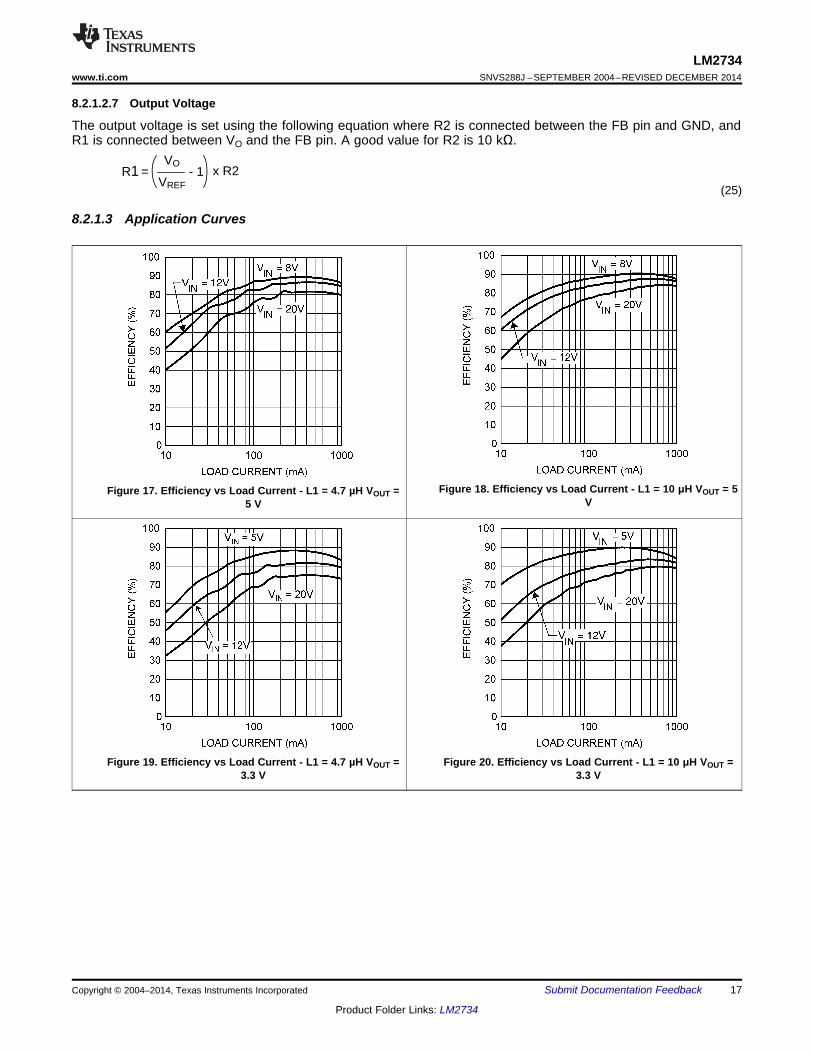
8.2.1.3 Application Curves
Figure 18. Efficiency vs Load Current - L1 = 10 μH VOUT = 5Figure 17. Efficiency vs Load Current - L1 = 4.7 µH VOUT =V5 V
Figure 19. Efficiency vs Load Current - L1 = 4.7 µH VOUT = Figure 20. Efficiency vs Load Current - L1 = 10 μH VOUT =3.3 V 3.3 V
LM2734SNVS288J –SEPTEMBER 2004–REVISED DECEMBER 2014 www.ti.com
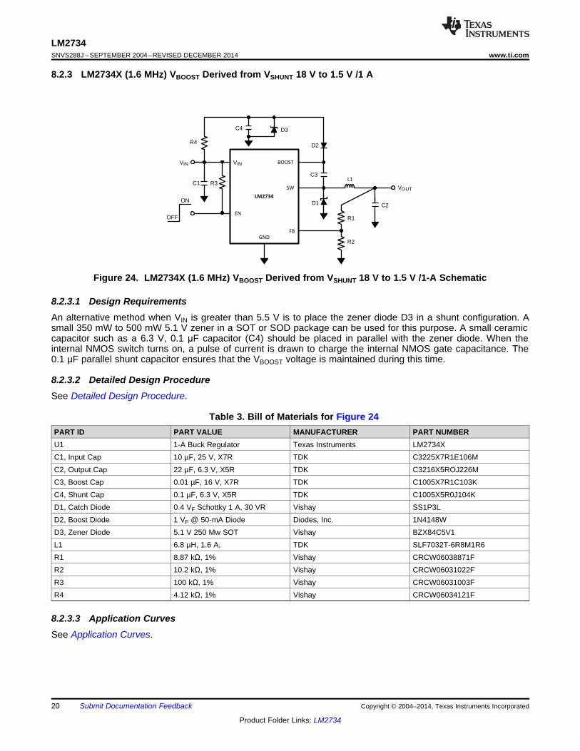
8.2.3 LM2734X (1.6 MHz) VBOOST Derived from VSHUNT 18 V to 1.5 V /1 A
Figure 24. LM2734X (1.6 MHz) VBOOST Derived from VSHUNT 18 V to 1.5 V /1-A Schematic
8.2.3.1 Design RequirementsAn alternative method when VIN is greater than 5.5 V is to place the zener diode D3 in a shunt configuration. Asmall 350 mW to 500 mW 5.1 V zener in a SOT or SOD package can be used for this purpose. A small ceramiccapacitor such as a 6.3 V, 0.1 μF capacitor (C4) should be placed in parallel with the zener diode. When theinternal NMOS switch turns on, a pulse of current is drawn to charge the internal NMOS gate capacitance. The0.1 μF parallel shunt capacitor ensures that the VBOOST voltage is maintained during this time.
LM2734www.ti.com SNVS288J –SEPTEMBER 2004–REVISED DECEMBER 2014
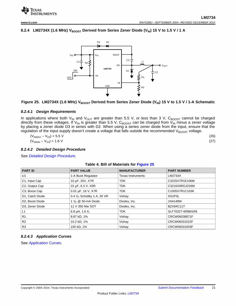
8.2.4 LM2734X (1.6 MHz) VBOOST Derived from Series Zener Diode (VIN) 15 V to 1.5 V / 1 A
Figure 25. LM2734X (1.6 MHz) VBOOST Derived from Series Zener Diode (VIN) 15 V to 1.5 V / 1-A Schematic
8.2.4.1 Design RequirementsIn applications where both VIN and VOUT are greater than 5.5 V, or less than 3 V, CBOOST cannot be chargeddirectly from these voltages. If VIN is greater than 5.5 V, CBOOST can be charged from VIN minus a zener voltageby placing a zener diode D3 in series with D2. When using a series zener diode from the input, ensure that theregulation of the input supply doesn’t create a voltage that falls outside the recommended VBOOST voltage.
(VINMAX – VD3) < 5.5 V (26)(VINMIN – VD3) > 1.6 V (27)
LM2734SNVS288J –SEPTEMBER 2004–REVISED DECEMBER 2014 www.ti.com
8.2.5 LM2734X (1.6 MHz) VBOOST Derived from Series Zener Diode (VOUT) 15 V to 9 V /1 A
Figure 26. LM2734X (1.6 MHz) VBOOST Derived from Series Zener Diode (VOUT) 15 V to 9 V /1-A Schematic
8.2.5.1 Design RequirementsIn applications where both VIN and VOUT are greater than 5.5 V, or less than 3 V, CBOOST cannot be chargeddirectly from these voltages. If VIN and VOUT are greater than 5.5 V, CBOOST can be charged from VOUT minus azener voltage by placing a zener diode D3 in series with D2.
LM2734www.ti.com SNVS288J –SEPTEMBER 2004–REVISED DECEMBER 2014
8.2.8 LM2734Y (550 kHz) VBOOST Derived from VSHUNT 18 V to 1.5 V / 1 A
Figure 29. LM2734Y (550 kHz) VBOOST Derived from VSHUNT 18 V to 1.5 V / 1-A
8.2.8.1 Design RequirementsAn alternative method when VIN is greater than 5.5 V is to place the zener diode D3 in a shunt configuration. Asmall 350 mW to 500 mW 5.1 V zener in a SOT or SOD package can be used for this purpose. A small ceramiccapacitor such as a 6.3 V, 0.1 μF capacitor (C4) should be placed in parallel with the zener diode. When theinternal NMOS switch turns on, a pulse of current is drawn to charge the internal NMOS gate capacitance. The0.1 μF parallel shunt capacitor ensures that the VBOOST voltage is maintained during this time.
LM2734SNVS288J –SEPTEMBER 2004–REVISED DECEMBER 2014 www.ti.com
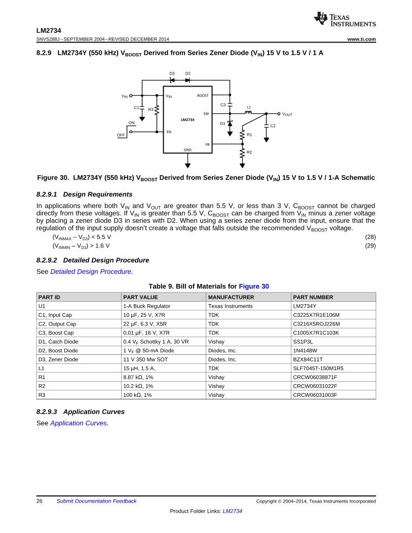
8.2.9 LM2734Y (550 kHz) VBOOST Derived from Series Zener Diode (VIN) 15 V to 1.5 V / 1 A
Figure 30. LM2734Y (550 kHz) VBOOST Derived from Series Zener Diode (VIN) 15 V to 1.5 V / 1-A Schematic
8.2.9.1 Design RequirementsIn applications where both VIN and VOUT are greater than 5.5 V, or less than 3 V, CBOOST cannot be chargeddirectly from these voltages. If VIN is greater than 5.5 V, CBOOST can be charged from VIN minus a zener voltageby placing a zener diode D3 in series with D2. When using a series zener diode from the input, ensure that theregulation of the input supply doesn’t create a voltage that falls outside the recommended VBOOST voltage.
(VINMAX – VD3) < 5.5 V (28)(VINMIN – VD3) > 1.6 V (29)
LM2734www.ti.com SNVS288J –SEPTEMBER 2004–REVISED DECEMBER 2014
8.2.10 LM2734Y (550 kHz) VBOOST Derived from Series Zener Diode (VOUT) 15 V to 9 V / 1 A
Figure 31. LM2734Y (550 kHz) VBOOST Derived from Series Zener Diode (VOUT) 15 V to 9 V / 1-A
8.2.10.1 Design RequirementsIn applications where both VIN and VOUT are greater than 5.5 V, or less than 3 V, CBOOST cannot be chargeddirectly from these voltages. If VIN and VOUT are greater than 5.5 V, CBOOST can be charged from VOUT minus azener voltage by placing a zener diode D3 in series with D2.
LM2734SNVS288J –SEPTEMBER 2004–REVISED DECEMBER 2014 www.ti.com
9 Power Supply RecommendationsInput voltage is rated as 3 V to 18 V; however, care must be taken in certain circuit configurations (for example,VBOOST derived from VIN where the requirement that VBOOST - VSW < 5.5 V should be observed) Also, for bestefficiency VBOOST should be at least 2.5-V above VSW.
The voltage on the Enable pin should not exceed VIN by more than 0.3 V.
10 Layout
10.1 Layout GuidelinesWhen planning layout there are a few things to consider when trying to achieve a clean, regulated output. Themost important consideration when completing the layout is the close coupling of the GND connections of the CINcapacitor and the catch diode D1. These ground ends should be close to one another and be connected to theGND plane with at least two through-holes. Place these components as close to the IC as possible. Next inimportance is the location of the GND connection of the COUT capacitor, which should be near the GNDconnections of CIN and D1.
There should be a continuous ground plane on the bottom layer of a two-layer board except under the switchingnode island.
The FB pin is a high-impedance node and care should be taken to make the FB trace short to avoid noise pickupand inaccurate regulation. The feedback resistors should be placed as close as possible to the IC, with the GNDof R2 placed as close as possible to the GND of the IC. The VOUT trace to R1 should be routed away from theinductor and any other traces that are switching.
High AC currents flow through the VIN, SW and VOUT traces, so they should be as short and wide as possible.However, making the traces wide increases radiated noise, so the designer must make this trade-off. Radiatednoise can be decreased by choosing a shielded inductor.
The remaining components should also be placed as close as possible to the IC. See Application Note AN-1229(SNVA054) for further considerations and the LM2734 demo board as an example of a four-layer layout.
LM2734SNVS288J –SEPTEMBER 2004–REVISED DECEMBER 2014 www.ti.com
11 Device and Documentation Support
11.1 Third-Party Products DisclaimerTI'S PUBLICATION OF INFORMATION REGARDING THIRD-PARTY PRODUCTS OR SERVICES DOES NOTCONSTITUTE AN ENDORSEMENT REGARDING THE SUITABILITY OF SUCH PRODUCTS OR SERVICESOR A WARRANTY, REPRESENTATION OR ENDORSEMENT OF SUCH PRODUCTS OR SERVICES, EITHERALONE OR IN COMBINATION WITH ANY TI PRODUCT OR SERVICE.
11.2 TrademarksWEBENCH is a registered trademark of Texas Instruments.All other trademarks are the property of their respective owners.
11.3 Electrostatic Discharge CautionThese devices have limited built-in ESD protection. The leads should be shorted together or the device placed in conductive foamduring storage or handling to prevent electrostatic damage to the MOS gates.
11.4 GlossarySLYZ022 — TI Glossary.
This glossary lists and explains terms, acronyms, and definitions.
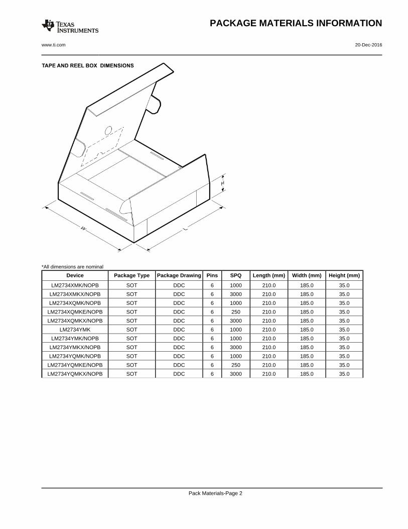
12 Mechanical, Packaging, and Orderable InformationThe following pages include mechanical, packaging, and orderable information. This information is the mostcurrent data available for the designated devices. This data is subject to change without notice and revision ofthis document. For browser-based versions of this data sheet, refer to the left-hand navigation.
LM2734XMK/NOPB ACTIVE SOT DDC 6 1000 Green (RoHS& no Sb/Br)
CU SN Level-1-260C-UNLIM -40 to 125 SFDB
LM2734XMKX/NOPB ACTIVE SOT DDC 6 3000 Green (RoHS& no Sb/Br)
CU SN Level-1-260C-UNLIM -40 to 125 SFDB
LM2734XQMK/NOPB ACTIVE SOT DDC 6 1000 Green (RoHS& no Sb/Br)
CU SN Level-1-260C-UNLIM -40 to 125 SUKB
LM2734XQMKE/NOPB ACTIVE SOT DDC 6 250 Green (RoHS& no Sb/Br)
CU SN Level-1-260C-UNLIM -40 to 125 SUKB
LM2734XQMKX/NOPB ACTIVE SOT DDC 6 3000 Green (RoHS& no Sb/Br)
CU SN Level-1-260C-UNLIM -40 to 125 SUKB
LM2734YMK NRND SOT DDC 6 1000 TBD Call TI Call TI -40 to 125 SFEB
LM2734YMK/NOPB ACTIVE SOT DDC 6 1000 Green (RoHS& no Sb/Br)
CU SN Level-1-260C-UNLIM -40 to 125 SFEB
LM2734YMKX/NOPB ACTIVE SOT DDC 6 3000 Green (RoHS& no Sb/Br)
CU SN Level-1-260C-UNLIM -40 to 125 SFEB
LM2734YQMK/NOPB ACTIVE SOT DDC 6 1000 Green (RoHS& no Sb/Br)
CU SN Level-1-260C-UNLIM -40 to 125 SVCB
LM2734YQMKE/NOPB ACTIVE SOT DDC 6 250 Green (RoHS& no Sb/Br)
CU SN Level-1-260C-UNLIM -40 to 125 SVCB
LM2734YQMKX/NOPB ACTIVE SOT DDC 6 3000 Green (RoHS& no Sb/Br)
CU SN Level-1-260C-UNLIM -40 to 125 SVCB
(1) The marketing status values are defined as follows:ACTIVE: Product device recommended for new designs.LIFEBUY: TI has announced that the device will be discontinued, and a lifetime-buy period is in effect.NRND: Not recommended for new designs. Device is in production to support existing customers, but TI does not recommend using this part in a new design.PREVIEW: Device has been announced but is not in production. Samples may or may not be available.OBSOLETE: TI has discontinued the production of the device.
(2) Eco Plan - The planned eco-friendly classification: Pb-Free (RoHS), Pb-Free (RoHS Exempt), or Green (RoHS & no Sb/Br) - please check http://www.ti.com/productcontent for the latest availabilityinformation and additional product content details.TBD: The Pb-Free/Green conversion plan has not been defined.Pb-Free (RoHS): TI's terms "Lead-Free" or "Pb-Free" mean semiconductor products that are compatible with the current RoHS requirements for all 6 substances, including the requirement thatlead not exceed 0.1% by weight in homogeneous materials. Where designed to be soldered at high temperatures, TI Pb-Free products are suitable for use in specified lead-free processes.Pb-Free (RoHS Exempt): This component has a RoHS exemption for either 1) lead-based flip-chip solder bumps used between the die and package, or 2) lead-based die adhesive used betweenthe die and leadframe. The component is otherwise considered Pb-Free (RoHS compatible) as defined above.
Green (RoHS & no Sb/Br): TI defines "Green" to mean Pb-Free (RoHS compatible), and free of Bromine (Br) and Antimony (Sb) based flame retardants (Br or Sb do not exceed 0.1% by weightin homogeneous material)
(3) MSL, Peak Temp. - The Moisture Sensitivity Level rating according to the JEDEC industry standard classifications, and peak solder temperature.
(4) There may be additional marking, which relates to the logo, the lot trace code information, or the environmental category on the device.
(5) Multiple Device Markings will be inside parentheses. Only one Device Marking contained in parentheses and separated by a "~" will appear on a device. If a line is indented then it is a continuationof the previous line and the two combined represent the entire Device Marking for that device.
(6) Lead/Ball Finish - Orderable Devices may have multiple material finish options. Finish options are separated by a vertical ruled line. Lead/Ball Finish values may wrap to two lines if the finishvalue exceeds the maximum column width.
Important Information and Disclaimer:The information provided on this page represents TI's knowledge and belief as of the date that it is provided. TI bases its knowledge and belief on informationprovided by third parties, and makes no representation or warranty as to the accuracy of such information. Efforts are underway to better integrate information from third parties. TI has taken andcontinues to take reasonable steps to provide representative and accurate information but may not have conducted destructive testing or chemical analysis on incoming materials and chemicals.TI and TI suppliers consider certain information to be proprietary, and thus CAS numbers and other limited information may not be available for release.
In no event shall TI's liability arising out of such information exceed the total purchase price of the TI part(s) at issue in this document sold by TI to Customer on an annual basis.
OTHER QUALIFIED VERSIONS OF LM2734, LM2734-Q1 :
• Catalog: LM2734
• Automotive: LM2734-Q1
NOTE: Qualified Version Definitions:
• Catalog - TI's standard catalog product
• Automotive - Q100 devices qualified for high-reliability automotive applications targeting zero defects
Texas Instruments Incorporated and its subsidiaries (TI) reserve the right to make corrections, enhancements, improvements and otherchanges to its semiconductor products and services per JESD46, latest issue, and to discontinue any product or service per JESD48, latestissue. Buyers should obtain the latest relevant information before placing orders and should verify that such information is current andcomplete. All semiconductor products (also referred to herein as “components”) are sold subject to TI’s terms and conditions of salesupplied at the time of order acknowledgment.TI warrants performance of its components to the specifications applicable at the time of sale, in accordance with the warranty in TI’s termsand conditions of sale of semiconductor products. Testing and other quality control techniques are used to the extent TI deems necessaryto support this warranty. Except where mandated by applicable law, testing of all parameters of each component is not necessarilyperformed.TI assumes no liability for applications assistance or the design of Buyers’ products. Buyers are responsible for their products andapplications using TI components. To minimize the risks associated with Buyers’ products and applications, Buyers should provideadequate design and operating safeguards.TI does not warrant or represent that any license, either express or implied, is granted under any patent right, copyright, mask work right, orother intellectual property right relating to any combination, machine, or process in which TI components or services are used. Informationpublished by TI regarding third-party products or services does not constitute a license to use such products or services or a warranty orendorsement thereof. Use of such information may require a license from a third party under the patents or other intellectual property of thethird party, or a license from TI under the patents or other intellectual property of TI.Reproduction of significant portions of TI information in TI data books or data sheets is permissible only if reproduction is without alterationand is accompanied by all associated warranties, conditions, limitations, and notices. TI is not responsible or liable for such altereddocumentation. Information of third parties may be subject to additional restrictions.Resale of TI components or services with statements different from or beyond the parameters stated by TI for that component or servicevoids all express and any implied warranties for the associated TI component or service and is an unfair and deceptive business practice.TI is not responsible or liable for any such statements.Buyer acknowledges and agrees that it is solely responsible for compliance with all legal, regulatory and safety-related requirementsconcerning its products, and any use of TI components in its applications, notwithstanding any applications-related information or supportthat may be provided by TI. Buyer represents and agrees that it has all the necessary expertise to create and implement safeguards whichanticipate dangerous consequences of failures, monitor failures and their consequences, lessen the likelihood of failures that might causeharm and take appropriate remedial actions. Buyer will fully indemnify TI and its representatives against any damages arising out of the useof any TI components in safety-critical applications.In some cases, TI components may be promoted specifically to facilitate safety-related applications. With such components, TI’s goal is tohelp enable customers to design and create their own end-product solutions that meet applicable functional safety standards andrequirements. Nonetheless, such components are subject to these terms.No TI components are authorized for use in FDA Class III (or similar life-critical medical equipment) unless authorized officers of the partieshave executed a special agreement specifically governing such use.Only those TI components which TI has specifically designated as military grade or “enhanced plastic” are designed and intended for use inmilitary/aerospace applications or environments. Buyer acknowledges and agrees that any military or aerospace use of TI componentswhich have not been so designated is solely at the Buyer's risk, and that Buyer is solely responsible for compliance with all legal andregulatory requirements in connection with such use.TI has specifically designated certain components as meeting ISO/TS16949 requirements, mainly for automotive use. In any case of use ofnon-designated products, TI will not be responsible for any failure to meet ISO/TS16949.
Products ApplicationsAudio www.ti.com/audio Automotive and Transportation www.ti.com/automotiveAmplifiers amplifier.ti.com Communications and Telecom www.ti.com/communicationsData Converters dataconverter.ti.com Computers and Peripherals www.ti.com/computersDLP® Products www.dlp.com Consumer Electronics www.ti.com/consumer-appsDSP dsp.ti.com Energy and Lighting www.ti.com/energyClocks and Timers www.ti.com/clocks Industrial www.ti.com/industrialInterface interface.ti.com Medical www.ti.com/medicalLogic logic.ti.com Security www.ti.com/securityPower Mgmt power.ti.com Space, Avionics and Defense www.ti.com/space-avionics-defenseMicrocontrollers microcontroller.ti.com Video and Imaging www.ti.com/videoRFID www.ti-rfid.comOMAP Applications Processors www.ti.com/omap TI E2E Community e2e.ti.comWireless Connectivity www.ti.com/wirelessconnectivity