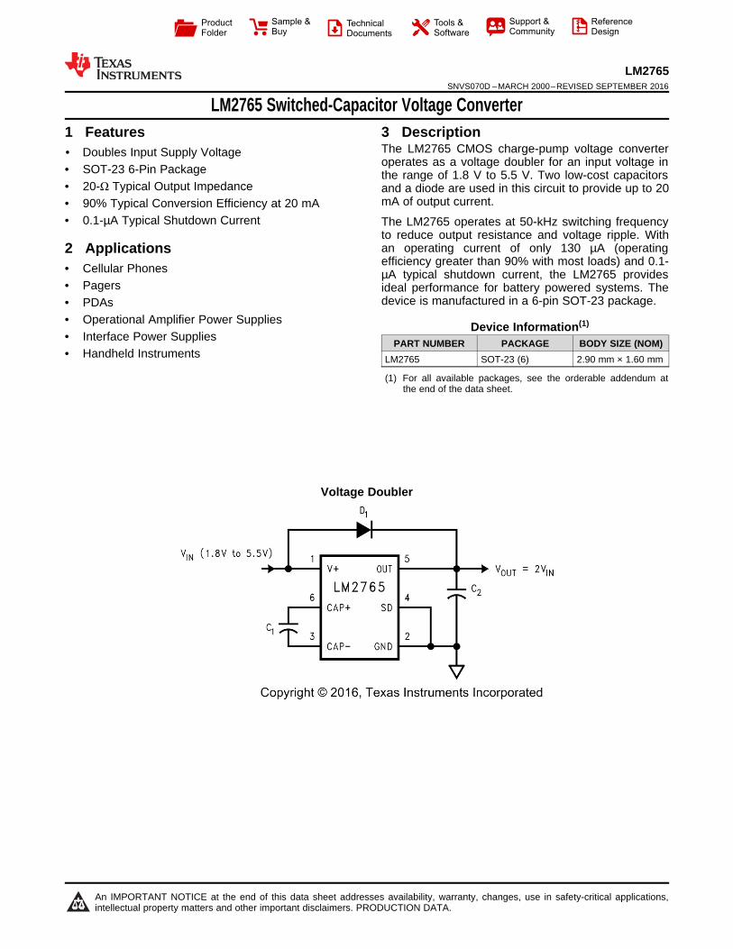
Product Folder Sample & Buy Technical Documents Tools & Software Support & Community Reference Design An IMPORTANT NOTICE at the end of this data sheet addresses availability, warranty, changes, use in safety-critical applications, intellectual property matters and other important disclaimers. PRODUCTION DATA. LM2765 SNVS070D – MARCH 2000 – REVISED SEPTEMBER 2016 LM2765 Switched-Capacitor Voltage Converter 1 1 Features 1• Doubles Input Supply Voltage • SOT-23 6-Pin Package • 20-Ω Typical Output Impedance • 90% Typical Conversion Efficiency at 20 mA • 0.1-μA Typical Shutdown Current 2 Applications • Cellular Phones • Pagers • PDAs • Operational Amplifier Power Supplies • Interface Power Supplies • Handheld Instruments 3 Description The LM2765 CMOS charge-pump voltage converter operates as a voltage doubler for an input voltage in the range of 1.8 V to 5.5 V. Two low-cost capacitors and a diode are used in this circuit to provide up to 20 mA of output current. The LM2765 operates at 50-kHz switching frequency to reduce output resistance and voltage ripple. With an operating current of only 130 μA (operating efficiency greater than 90% with most loads) and 0.1- μA typical shutdown current, the LM2765 provides ideal performance for battery powered systems. The device is manufactured in a 6-pin SOT-23 package. Device Information (1) PART NUMBER PACKAGE BODY SIZE (NOM) LM2765 SOT-23 (6) 2.90 mm × 1.60 mm (1) For all available packages, see the orderable addendum at the end of the data sheet. space space space space Voltage Doubler
Transcript
Product
Folder
Sample &Buy
Technical
Documents
Tools &
Software
Support &Community
ReferenceDesign
An IMPORTANT NOTICE at the end of this data sheet addresses availability, warranty, changes, use in safety-critical applications,intellectual property matters and other important disclaimers. PRODUCTION DATA.
2 Applications• Cellular Phones• Pagers• PDAs• Operational Amplifier Power Supplies• Interface Power Supplies• Handheld Instruments
3 DescriptionThe LM2765 CMOS charge-pump voltage converteroperates as a voltage doubler for an input voltage inthe range of 1.8 V to 5.5 V. Two low-cost capacitorsand a diode are used in this circuit to provide up to 20mA of output current.
The LM2765 operates at 50-kHz switching frequencyto reduce output resistance and voltage ripple. Withan operating current of only 130 µA (operatingefficiency greater than 90% with most loads) and 0.1-µA typical shutdown current, the LM2765 providesideal performance for battery powered systems. Thedevice is manufactured in a 6-pin SOT-23 package.
Device Information(1)
PART NUMBER PACKAGE BODY SIZE (NOM)LM2765 SOT-23 (6) 2.90 mm × 1.60 mm
(1) For all available packages, see the orderable addendum atthe end of the data sheet.
10 Power Supply Recommendations ..................... 1211 Layout................................................................... 13
11.1 Layout Guidelines ................................................. 1311.2 Layout Example .................................................... 13
12 Device and Documentation Support ................. 1412.1 Device Support...................................................... 1412.2 Receiving Notification of Documentation Updates 1412.3 Community Resources.......................................... 1412.4 Trademarks ........................................................... 1412.5 Electrostatic Discharge Caution............................ 1412.6 Glossary ................................................................ 14
13 Mechanical, Packaging, and OrderableInformation ........................................................... 14
4 Revision HistoryNOTE: Page numbers for previous revisions may differ from page numbers in the current version.
Changes from Revision C (May 2013) to Revision D Page
• Added Pin Configuration and Functions section, ESD Rating table, Feature Description , Device Functional Modes,Application and Implementation, Power Supply Recommendations, Layout, Device and Documentation Support, andMechanical, Packaging, and Orderable Information sections; change pin name "VOUT" to "OUT"...................................... 1
• Added top nav icon for TI design .......................................................................................................................................... 1• Changed RθJA value from 210°C/W to 185.2°C/W; add additional thermal values ................................................................ 4
Changes from Revision B (May 2013) to Revision C Page
• Changed layout of National Semiconductor data sheet to TI format.................................................................................... 12
TYPE DESCRIPTIONNO. NAME1 V+ Power Power supply positive voltage input2 GND Ground Power supply ground input3 CAP− Power Connect this pin to the negative terminal of the charge-pump capacitor.4 SD Input Shutdown control pin; tie this pin to ground in normal operation.5 OUT Power Positive voltage output6 CAP+ Power Connect this pin to the positive terminal of the charge-pump capacitor.
(1) Stresses beyond those listed under Absolute Maximum Ratings may cause permanent damage to the device. These are stress ratingsonly, which do not imply functional operation of the device at these or any other conditions beyond those indicated under RecommendedOperating Conditions. Exposure to absolute-maximum-rated conditions for extended periods may affect device reliability.
(2) If Military/Aerospace specified devices are required, contact the Texas Instruments Sales Office/ Distributors for availability andspecifications.
(3) OUT may be shorted to GND for one second without damage. However, shorting OUT to V+ may damage the device and must beavoided. Also, for temperatures above 85°C, OUT must not be shorted to GND or V+, or device may be damaged.
(4) The maximum allowable power dissipation is calculated by using PD-MAX = (TJ-MAX − TA)/RθJA, where TJ-MAX is the maximum junctiontemperature, TA is the ambient temperature, and RθJA is the junction-to-ambient thermal resistance of the specified package.
6 Specifications
6.1 Absolute Maximum Ratingsover operating free-air temperature range (unless otherwise noted) (1) (2)
MIN MAX UNITSupply voltage (V+ to GND or V+ to OUT) 5.8 VSD (GND − 0.3 V) (V+ + 0.3 V)OUT continuous output current 40 mAOutput short-circuit duration to GND (3) 1 secContinuous power dissipation (TA = 25°C) (4) 600 mWTJ-MAX
(4) 150 °CStorage temperature, Tstg −65 150 °C
(1) JEDEC document JEP155 states that 500-V HBM allows safe manufacturing with a standard ESD control process.
6.2 ESD RatingsVALUE UNIT
V(ESD) Electrostatic dischargeHuman-body model (HBM), per ANSI/ESDA/JEDEC JS-001 (1) ±2000 VMachine model 200 V
6.3 Recommended Operating Conditionsover operating free-air temperature range (unless otherwise noted)
MIN NOM MAX UNITAmbient temperature –40 85 °CJunction temperature –40 100 °C
(1) For more information about traditional and new thermal metrics, see the Semiconductor and IC Package Thermal Metrics applicationreport.
(1) In the test circuit, capacitors C1 and C2 are 3.3-µF, 0.3-Ω maximum ESR capacitors. Capacitors with higher ESR increase outputresistance, reduce output voltage, and efficiency.
(2) Specified output resistance includes internal switch resistance and capacitor ESR. See the details in Application and Implementation forsimple negative voltage converter.
(3) The output switches operate at one half of the oscillator frequency, ƒOSC = 2ƒSW.
6.5 Electrical CharacteristicsMIN and MAX limits apply over the full operating temperature range. Unless otherwise specified: TJ = 25°C, V+ = 5 V,C1 = C2 = 3.3 μF. (1)
PARAMETER TEST CONDITIONS MIN TYP MAX UNITV+ Supply voltage 1.8 5.5 VIQ Supply current No load 130 450 µA
ISD Shutdown supply current0.1 0.5
µATA = 85°C 0.2
VSD Shutdown pin input voltageShutdown mode 2
VNormal operation 0.6
IL Output current2.5 V ≤ VIN ≤ 5.5 V 20
mA1.8 V ≤ VIN ≤ 2.5 V 10
ROUT Output resistance (2) IL = 20 mA 20 40 Ω
ƒOSC Oscillator frequency See (3) 40 100 200 kHzƒSW Switching frequency See (3) 20 50 100 kHzPEFF Power efficiency RL (1 kΩ) between GND and OUT 92%VOEFF Voltage conversion efficiency No load 99.96%
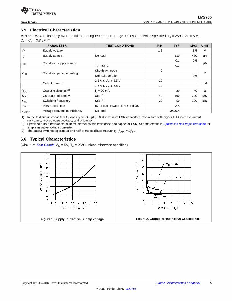
6.6 Typical Characteristics(Circuit of Test Circuit, VIN = 5V, TA = 25°C unless otherwise specified)
Figure 1. Supply Current vs Supply Voltage Figure 2. Output Resistance vs Capacitance
8.1 OverviewThe LM2765 CMOS charge-pump voltage converter operates as a voltage doubler for an input voltage in therange of 1.8 V to 5.5 V. Two low-cost capacitors and a diode (needed during start-up) are used in this circuit toprovide up to 20 mA of output current.
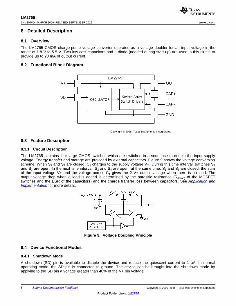
8.2 Functional Block Diagram
8.3 Feature Description
8.3.1 Circuit DescriptionThe LM2765 contains four large CMOS switches which are switched in a sequence to double the input supplyvoltage. Energy transfer and storage are provided by external capacitors. Figure 9 shows the voltage conversionscheme. When S2 and S4 are closed, C1 charges to the supply voltage V+. During this time interval, switches S1and S3 are open. In the next time interval, S2 and S4 are open; at the same time, S1 and S3 are closed, the sumof the input voltage V+ and the voltage across C1 gives the 2 V+ output voltage when there is no load. Theoutput voltage drop when a load is added is determined by the parasitic resistance (Rds(on) of the MOSFETswitches and the ESR of the capacitors) and the charge transfer loss between capacitors. See Application andImplementation for more details.
Figure 9. Voltage Doubling Principle
8.4 Device Functional Modes
8.4.1 Shutdown ModeA shutdown (SD) pin is available to disable the device and reduce the quiescent current to 1 µA. In normaloperating mode, the SD pin is connected to ground. The device can be brought into the shutdown mode byapplying to the SD pin a voltage greater than 40% of the V+ pin voltage.
NOTEInformation in the following applications sections is not part of the TI componentspecification, and TI does not warrant its accuracy or completeness. TI’s customers areresponsible for determining suitability of components for their purposes. Customers mustvalidate and test their design implementation to confirm system functionality.
9.1 Application InformationThe LM2765 provides a simple and efficient means of creating an output voltage level equal to twice that of theinput voltage. Without the need of an inductor, the application solution size can be reduced versus the magneticDC-DC converter solution.
9.2 Typical Applications
9.2.1 Voltage DoublerThe main application of the LM2765 is to double the input voltage. The range of the input supply voltage is 1.8 Vto 5.5 V.
Figure 10. Voltage Doubler
9.2.1.1 Design RequirementsExample requirements for LM2765 device applications:
DESIGN PARAMETER EXAMPLE VALUEInput voltage range 1.8 V to 5.5 V
Output current 0 mA to 20 mABoost switching frequency 20 kHz
The output characteristics of this circuit can be approximated by an ideal voltage source in series with aresistance. The voltage source equals 2 V+. The output resistance ROUT is a function of the ON resistance of theinternal MOSFET switches, the oscillator frequency, the capacitance and equivalent series resistance (ESR) ofC1 and C2. Since the switching current charging and discharging C1 is approximately twice as the output current,the effect of the ESR of the pumping capacitor C1 will be multiplied by four in the output resistance. The outputcapacitor C2 is charging and discharging at a current approximately equal to the output current, therefore, itsESR only counts when in the output resistance. A good approximation of ROUT is:
where• RSW is the sum of the ON resistance of the internal MOSFET switches shown in Figure 9. RSW is typically 8 Ω
for the LM2765. (1)
The peak-to-peak output voltage ripple is determined by the oscillator frequency, the capacitance and ESR of theoutput capacitor C2:
(2)
High capacitance, low-ESR capacitors can reduce both the output resistance and the voltage ripple.
The Schottky diode D1 is only needed for start-up. The internal oscillator circuit uses the OUT pin and the GNDpin. Voltage across OUT and GND must be larger than 1.8 V to insure the operation of the oscillator. Duringstart-up, D1 is used to charge up the voltage at the OUT pin to start the oscillator; also, it protects the device fromturning-on its own parasitic diode and potentially latching-up. Therefore, the Schottky diode D1 must haveenough current carrying capability to charge the output capacitor at start-up, as well as a low forward voltage toprevent the internal parasitic diode from turning-on. A Schottky diode such as 1N5817 can be used for mostapplications. If the input voltage ramp is less than 10 V/ms, a smaller Schottky diode such as MBR0520LT1 canbe used to reduce the circuit size.
9.2.1.2.2 Capacitor Selection
As discussed in Positive Voltage Doubler, the output resistance and ripple voltage are dependent on thecapacitance and ESR values of the external capacitors. The output voltage drop is the load current times theoutput resistance, and the power efficiency is:
where• IQ(V+) is the quiescent power loss of the device; and• IL2Rout is the conversion loss associated with the switch on-resistance, the two external capacitors and their
ESRs. (3)
The selection of capacitors is based on the specifications of the dropout voltage (which equals IOUT ROUT), theoutput voltage ripple, and the converter efficiency. Low ESR capacitors are recommended to maximize efficiency,reduce the output voltage drop and voltage ripple.
9.2.1.2.3 Paralleling Devices
Any number of LM2765 devices can be paralleled to reduce the output resistance. Each device must have itsown pumping capacitor C1, while only one output capacitor, COUT, is required as shown in Figure 11. Thecomposite output resistance is:
ROUT = ROUT of each LM2765 / number of devices (4)
Figure 11. Lowering Output Resistance by Paralleling Devices
9.2.1.2.4 Cascading Devices
Cascading the LM2765 devices is an easy way to produce a greater voltage (a two-stage cascade circuit isshown in Figure 12).
The effective output resistance is equal to the weighted sum of each individual device, shown in Equation 5:ROUT = 1.5 ROUT_1 + ROUT_2 (5)
Note that the increasing of the number of cascading stages is practically limited since it significantly reduces theefficiency, increases the output resistance and output voltage ripple.
Figure 12. Increasing Output Voltage by Cascading Devices
9.2.1.2.5 Regulating VOUT
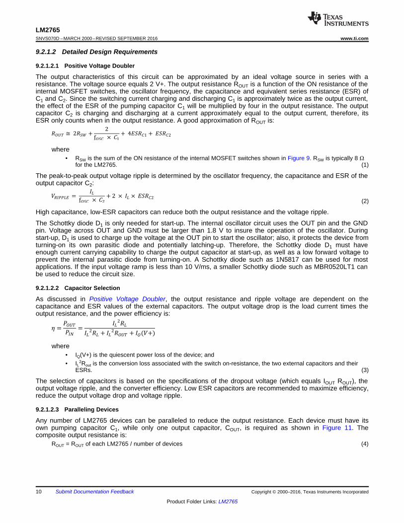
It is possible to regulate the output of the LM2765 by use of a low dropout regulator (such as LP2980-5.0). Thewhole converter is depicted in Figure 13.
A different output voltage is possible by use of LP2980-3.3, LP2980-3.0, or LP2980-ADJ.
Note that the following conditions must be satisfied simultaneously for worst-case design:2Vin_min > Vout_min + Vdrop_max (LP2980) + Iout_max × Rout_max (LM2765) (6)2Vin_max < Vout_max + Vdrop_min (LP2980) + Iout_min × Rout_min (LM2765) (7)
Figure 13. Generating a Regulated +5-V From +3-V Input Voltage
9.2.1.3 Application Curve
Figure 14. Efficiency vs Load Current
10 Power Supply RecommendationsThe LM2765 is designed to operate from as an inverter over an input voltage supply range between 1.8 V and5.5 V. This input supply must be well regulated and capable to supply the required input current. If the inputsupply is located far from the device, additional bulk capacitance may be required in addition to the ceramicbypass capacitors.
11.1 Layout GuidelinesThe high switching frequency and large switching currents of the LM2765 make the choice of layout important.Use the following steps as a reference to ensure the device is stable and maintains proper LED currentregulation across its intended operating voltage and current range.• Place CIN on the top layer (same layer as the LM2765) and as close as possible to the device. Connecting
the input capacitor through short, wide traces to both the V+ and GND pins reduces the inductive voltagespikes that occur during switching which can corrupt the V+ line.
• Place COUT on the top layer (same layer as the LM2765) and as close as possible to the OUT and GND pin.The returns for both CIN and COUT must come together at one point, as close as possible to the GND pin.Connecting COUT through short, wide traces reduce the series inductance on the OUT and GND pins that cancorrupt the VOUT and GND lines and cause excessive noise in the device and surrounding circuitry.
• Place C1 on the top layer (same layer as the LM2765 device) and as close as possible to the device.Connect the flying capacitor through short, wide traces to both the CAP+ and CAP– pins.
12.1.1 Third-Party Products DisclaimerTI'S PUBLICATION OF INFORMATION REGARDING THIRD-PARTY PRODUCTS OR SERVICES DOES NOTCONSTITUTE AN ENDORSEMENT REGARDING THE SUITABILITY OF SUCH PRODUCTS OR SERVICESOR A WARRANTY, REPRESENTATION OR ENDORSEMENT OF SUCH PRODUCTS OR SERVICES, EITHERALONE OR IN COMBINATION WITH ANY TI PRODUCT OR SERVICE.
12.2 Receiving Notification of Documentation UpdatesTo receive notification of documentation updates, navigate to the device product folder on ti.com. In the upperright corner, click on Alert me to register and receive a weekly digest of any product information that haschanged. For change details, review the revision history included in any revised document.
12.3 Community ResourcesThe following links connect to TI community resources. Linked contents are provided "AS IS" by the respectivecontributors. They do not constitute TI specifications and do not necessarily reflect TI's views; see TI's Terms ofUse.
TI E2E™ Online Community TI's Engineer-to-Engineer (E2E) Community. Created to foster collaborationamong engineers. At e2e.ti.com, you can ask questions, share knowledge, explore ideas and helpsolve problems with fellow engineers.
Design Support TI's Design Support Quickly find helpful E2E forums along with design support tools andcontact information for technical support.
12.4 TrademarksE2E is a trademark of Texas Instruments.All other trademarks are the property of their respective owners.
12.5 Electrostatic Discharge CautionThese devices have limited built-in ESD protection. The leads should be shorted together or the device placed in conductive foamduring storage or handling to prevent electrostatic damage to the MOS gates.
12.6 GlossarySLYZ022 — TI Glossary.
This glossary lists and explains terms, acronyms, and definitions.
13 Mechanical, Packaging, and Orderable InformationThe following pages include mechanical, packaging, and orderable information. This information is the mostcurrent data available for the designated devices. This data is subject to change without notice and revision ofthis document. For browser-based versions of this data sheet, refer to the left-hand navigation.
LM2765M6X/NOPB ACTIVE SOT-23 DBV 6 3000 Green (RoHS& no Sb/Br)
CU SN Level-1-260C-UNLIM -40 to 85 S15B
(1) The marketing status values are defined as follows:ACTIVE: Product device recommended for new designs.LIFEBUY: TI has announced that the device will be discontinued, and a lifetime-buy period is in effect.NRND: Not recommended for new designs. Device is in production to support existing customers, but TI does not recommend using this part in a new design.PREVIEW: Device has been announced but is not in production. Samples may or may not be available.OBSOLETE: TI has discontinued the production of the device.
(2) Eco Plan - The planned eco-friendly classification: Pb-Free (RoHS), Pb-Free (RoHS Exempt), or Green (RoHS & no Sb/Br) - please check http://www.ti.com/productcontent for the latest availabilityinformation and additional product content details.TBD: The Pb-Free/Green conversion plan has not been defined.Pb-Free (RoHS): TI's terms "Lead-Free" or "Pb-Free" mean semiconductor products that are compatible with the current RoHS requirements for all 6 substances, including the requirement thatlead not exceed 0.1% by weight in homogeneous materials. Where designed to be soldered at high temperatures, TI Pb-Free products are suitable for use in specified lead-free processes.Pb-Free (RoHS Exempt): This component has a RoHS exemption for either 1) lead-based flip-chip solder bumps used between the die and package, or 2) lead-based die adhesive used betweenthe die and leadframe. The component is otherwise considered Pb-Free (RoHS compatible) as defined above.Green (RoHS & no Sb/Br): TI defines "Green" to mean Pb-Free (RoHS compatible), and free of Bromine (Br) and Antimony (Sb) based flame retardants (Br or Sb do not exceed 0.1% by weightin homogeneous material)
(3) MSL, Peak Temp. - The Moisture Sensitivity Level rating according to the JEDEC industry standard classifications, and peak solder temperature.
(4) There may be additional marking, which relates to the logo, the lot trace code information, or the environmental category on the device.
(5) Multiple Device Markings will be inside parentheses. Only one Device Marking contained in parentheses and separated by a "~" will appear on a device. If a line is indented then it is a continuationof the previous line and the two combined represent the entire Device Marking for that device.
(6) Lead/Ball Finish - Orderable Devices may have multiple material finish options. Finish options are separated by a vertical ruled line. Lead/Ball Finish values may wrap to two lines if the finishvalue exceeds the maximum column width.
Important Information and Disclaimer:The information provided on this page represents TI's knowledge and belief as of the date that it is provided. TI bases its knowledge and belief on informationprovided by third parties, and makes no representation or warranty as to the accuracy of such information. Efforts are underway to better integrate information from third parties. TI has taken andcontinues to take reasonable steps to provide representative and accurate information but may not have conducted destructive testing or chemical analysis on incoming materials and chemicals.TI and TI suppliers consider certain information to be proprietary, and thus CAS numbers and other limited information may not be available for release.
In no event shall TI's liability arising out of such information exceed the total purchase price of the TI part(s) at issue in this document sold by TI to Customer on an annual basis.
Texas Instruments Incorporated and its subsidiaries (TI) reserve the right to make corrections, enhancements, improvements and otherchanges to its semiconductor products and services per JESD46, latest issue, and to discontinue any product or service per JESD48, latestissue. Buyers should obtain the latest relevant information before placing orders and should verify that such information is current andcomplete. All semiconductor products (also referred to herein as “components”) are sold subject to TI’s terms and conditions of salesupplied at the time of order acknowledgment.TI warrants performance of its components to the specifications applicable at the time of sale, in accordance with the warranty in TI’s termsand conditions of sale of semiconductor products. Testing and other quality control techniques are used to the extent TI deems necessaryto support this warranty. Except where mandated by applicable law, testing of all parameters of each component is not necessarilyperformed.TI assumes no liability for applications assistance or the design of Buyers’ products. Buyers are responsible for their products andapplications using TI components. To minimize the risks associated with Buyers’ products and applications, Buyers should provideadequate design and operating safeguards.TI does not warrant or represent that any license, either express or implied, is granted under any patent right, copyright, mask work right, orother intellectual property right relating to any combination, machine, or process in which TI components or services are used. Informationpublished by TI regarding third-party products or services does not constitute a license to use such products or services or a warranty orendorsement thereof. Use of such information may require a license from a third party under the patents or other intellectual property of thethird party, or a license from TI under the patents or other intellectual property of TI.Reproduction of significant portions of TI information in TI data books or data sheets is permissible only if reproduction is without alterationand is accompanied by all associated warranties, conditions, limitations, and notices. TI is not responsible or liable for such altereddocumentation. Information of third parties may be subject to additional restrictions.Resale of TI components or services with statements different from or beyond the parameters stated by TI for that component or servicevoids all express and any implied warranties for the associated TI component or service and is an unfair and deceptive business practice.TI is not responsible or liable for any such statements.Buyer acknowledges and agrees that it is solely responsible for compliance with all legal, regulatory and safety-related requirementsconcerning its products, and any use of TI components in its applications, notwithstanding any applications-related information or supportthat may be provided by TI. Buyer represents and agrees that it has all the necessary expertise to create and implement safeguards whichanticipate dangerous consequences of failures, monitor failures and their consequences, lessen the likelihood of failures that might causeharm and take appropriate remedial actions. Buyer will fully indemnify TI and its representatives against any damages arising out of the useof any TI components in safety-critical applications.In some cases, TI components may be promoted specifically to facilitate safety-related applications. With such components, TI’s goal is tohelp enable customers to design and create their own end-product solutions that meet applicable functional safety standards andrequirements. Nonetheless, such components are subject to these terms.No TI components are authorized for use in FDA Class III (or similar life-critical medical equipment) unless authorized officers of the partieshave executed a special agreement specifically governing such use.Only those TI components which TI has specifically designated as military grade or “enhanced plastic” are designed and intended for use inmilitary/aerospace applications or environments. Buyer acknowledges and agrees that any military or aerospace use of TI componentswhich have not been so designated is solely at the Buyer's risk, and that Buyer is solely responsible for compliance with all legal andregulatory requirements in connection with such use.TI has specifically designated certain components as meeting ISO/TS16949 requirements, mainly for automotive use. In any case of use ofnon-designated products, TI will not be responsible for any failure to meet ISO/TS16949.
Products ApplicationsAudio www.ti.com/audio Automotive and Transportation www.ti.com/automotiveAmplifiers amplifier.ti.com Communications and Telecom www.ti.com/communicationsData Converters dataconverter.ti.com Computers and Peripherals www.ti.com/computersDLP® Products www.dlp.com Consumer Electronics www.ti.com/consumer-appsDSP dsp.ti.com Energy and Lighting www.ti.com/energyClocks and Timers www.ti.com/clocks Industrial www.ti.com/industrialInterface interface.ti.com Medical www.ti.com/medicalLogic logic.ti.com Security www.ti.com/securityPower Mgmt power.ti.com Space, Avionics and Defense www.ti.com/space-avionics-defenseMicrocontrollers microcontroller.ti.com Video and Imaging www.ti.com/videoRFID www.ti-rfid.comOMAP Applications Processors www.ti.com/omap TI E2E Community e2e.ti.comWireless Connectivity www.ti.com/wirelessconnectivity