GND FB EN VIN SW VIN = 5V C1 R3 D1 L1 R2 R1 C2 C3 VO = 3.3V @ 1.0A LM2830 Product Folder Sample & Buy Technical Documents Tools & Software Support & Community LM2830, LM2830-Q1 SNVS454E – AUGUST 2006 – REVISED DECEMBER 2014 LM2830/-Q1 High-Frequency 1.0-A Load Step-Down DC-DC Regulator 1 Features 3 Description The LM2830 regulator is a monolithic, high- 1• LM2830Z-Q1 and LM2830X-Q1 in the SOT-23 frequency, PWM step-down DC-DC converter in a 5- Package are Automotive-Grade Products that are pin SOT-23 and a 6-Pin WSON package. The device AEC-Q100 Grade 1 Qualified (–40°C to +125°C provides all the active functions to provide local DC- Operating Junction Temperature) DC conversion with fast transient response and • Space-Saving SOT-23 Package accurate regulation in the smallest possible PCB area. With a minimum of external components, the • Input Voltage Range of 3.0 V to 5.5 V LM2830 regulator is easy to use. The ability to drive • Output Voltage Range of 0.6 V to 4.5 V 1.0-A loads with an internal 130-mΩ PMOS switch • 1.0-A Output Current using state-of-the-art 0.5-μm BiCMOS technology • High Switching Frequencies results in the best power density available. The world- class control circuitry allows on-times as low as 30 – 1.6 MHz (LM2830X) ns, thus supporting exceptionally high frequency – 3.0 MHz (LM2830Z) conversion over the entire 3-V to 5.5-V input • 130-mΩ PMOS Switch operating range down to the minimum output voltage of 0.6 V. Switching frequency is internally set to 1.6 • 0.6-V, 2% Internal Voltage Reference MHz, or 3.0 MHz, allowing the use of extremely small • Internal Soft-Start surface-mount inductors and chip capacitors. Even • Current Mode, PWM Operation though the operating frequency is high, efficiencies up to 93% are easy to achieve. External shutdown is • Thermal Shutdown included, featuring an ultra-low standby current of 30 • Overvoltage Protection nA. The LM2830 regulator uses current-mode control and internal compensation to provide high- 2 Applications performance regulation over a wide range of operating conditions. Additional features include • Local 5-V to Vcore Step-Down Converters internal soft-start circuitry to reduce inrush current, • Core Power in HDDs pulse-by-pulse current limit, thermal shutdown, and • Set-Top Boxes output overvoltage protection. • USB Powered Devices Device Information (1) • DSL Modems PART NUMBER PACKAGE BODY SIZE (NOM) • Automotive SOT (5) 2.90 mm × 1.60 mm LM2830 WSON (6) 3.00 mm × 3.00 mm LM2830-Q1 SOT (5) 2.90 mm × 1.60 mm (1) For all available packages, see the orderable addendum at the end of the datasheet. Typical Application Circuit Efficiency vs Load Current 1 An IMPORTANT NOTICE at the end of this data sheet addresses availability, warranty, changes, use in safety-critical applications, intellectual property matters and other important disclaimers. PRODUCTION DATA.
Transcript
GND
FBEN
VIN SWVIN = 5V
C1
R3
D1
L1
R2
R1
C2 C3
VO = 3.3V @ 1.0A
LM2830
Product
Folder
Sample &Buy
Technical
Documents
Tools &
Software
Support &Community
LM2830, LM2830-Q1SNVS454E –AUGUST 2006–REVISED DECEMBER 2014
LM2830/-Q1 High-Frequency 1.0-A Load Step-Down DC-DC Regulator1 Features 3 Description
The LM2830 regulator is a monolithic, high-1• LM2830Z-Q1 and LM2830X-Q1 in the SOT-23
frequency, PWM step-down DC-DC converter in a 5-Package are Automotive-Grade Products that arepin SOT-23 and a 6-Pin WSON package. The deviceAEC-Q100 Grade 1 Qualified (–40°C to +125°C provides all the active functions to provide local DC-Operating Junction Temperature) DC conversion with fast transient response and
• Space-Saving SOT-23 Package accurate regulation in the smallest possible PCBarea. With a minimum of external components, the• Input Voltage Range of 3.0 V to 5.5 VLM2830 regulator is easy to use. The ability to drive• Output Voltage Range of 0.6 V to 4.5 V 1.0-A loads with an internal 130-mΩ PMOS switch
• 1.0-A Output Current using state-of-the-art 0.5-µm BiCMOS technology• High Switching Frequencies results in the best power density available. The world-
class control circuitry allows on-times as low as 30– 1.6 MHz (LM2830X)ns, thus supporting exceptionally high frequency
– 3.0 MHz (LM2830Z) conversion over the entire 3-V to 5.5-V input• 130-mΩ PMOS Switch operating range down to the minimum output voltage
of 0.6 V. Switching frequency is internally set to 1.6• 0.6-V, 2% Internal Voltage ReferenceMHz, or 3.0 MHz, allowing the use of extremely small• Internal Soft-Start surface-mount inductors and chip capacitors. Even
• Current Mode, PWM Operation though the operating frequency is high, efficienciesup to 93% are easy to achieve. External shutdown is• Thermal Shutdownincluded, featuring an ultra-low standby current of 30• Overvoltage ProtectionnA. The LM2830 regulator uses current-mode controland internal compensation to provide high-2 Applications performance regulation over a wide range ofoperating conditions. Additional features include• Local 5-V to Vcore Step-Down Convertersinternal soft-start circuitry to reduce inrush current,• Core Power in HDDspulse-by-pulse current limit, thermal shutdown, and• Set-Top Boxes output overvoltage protection.
• USB Powered DevicesDevice Information(1)• DSL Modems
PART NUMBER PACKAGE BODY SIZE (NOM)• AutomotiveSOT (5) 2.90 mm × 1.60 mm
LM2830WSON (6) 3.00 mm × 3.00 mm
LM2830-Q1 SOT (5) 2.90 mm × 1.60 mm
(1) For all available packages, see the orderable addendum atthe end of the datasheet.
Typical Application Circuit Efficiency vs Load Current
1
An IMPORTANT NOTICE at the end of this data sheet addresses availability, warranty, changes, use in safety-critical applications,intellectual property matters and other important disclaimers. PRODUCTION DATA.
LM2830, LM2830-Q1SNVS454E –AUGUST 2006–REVISED DECEMBER 2014 www.ti.com
Table of Contents7.4 Device Functional Modes........................................ 111 Features .................................................................. 1
12 Mechanical, Packaging, and Orderable7.3 Feature Description................................................. 10Information ........................................................... 29
4 Revision HistoryNOTE: Page numbers for previous revisions may differ from page numbers in the current version.
Changes from Revision D (April 2013) to Revision E Page
• Added Pin Configuration and Functions section, ESD Ratings table, Feature Description section, Device FunctionalModes, Application and Implementation section, Power Supply Recommendations section, Layout section, Deviceand Documentation Support section, and Mechanical, Packaging, and Orderable Information section .............................. 1
Changes from Revision C (April 2013) to Revision D Page
• Changed layout of National Data Sheet to TI format ........................................................................................................... 23
LM2830, LM2830-Q1www.ti.com SNVS454E –AUGUST 2006–REVISED DECEMBER 2014
5 Pin Configuration and Functions
WSON Package6-Pin
Top View
SOT Package5-Pins
Top View
Pin Functions (5-Pin SOT)PIN
I/O (1) DESCRIPTIONNAME NO.
SW 1 O Output switch. Connect to the inductor and catch diode.Signal and power ground pin. Place the bottom resistor of the feedback network as close asGND 2 G possible to this pin.
FB 3 I Feedback pin. Connect to external resistor divider to set output voltage.Enable control input. Logic high enables operation. Do not allow this pin to float or be greaterEN 4 I than VIN + 0.3 V.
FB 1 I Feedback pin. Connect to external resistor divider to set output voltage.Signal and power ground pin. Place the bottom resistor of the feedback network as close asGND 2 G possible to this pin.
SW 3 O Output switch. Connect to the inductor and catch diode.VIND 4 I/P Power Input supply.VINA 5 I/P Control circuitry supply voltage. Connect VINA to VIND on PC board.
Enable control input. Logic high enables operation. Do not allow this pin to float or be greaterEN 6 I than VINA + 0.3V.Die Attach Connect to system ground for low thermal impedance, but it cannot be used as a primary– –Pad GND connection.
LM2830, LM2830-Q1SNVS454E –AUGUST 2006–REVISED DECEMBER 2014 www.ti.com
6 Specifications
6.1 Absolute Maximum Ratings (1) (2)
MIN MAX UNITVIN –0.5 7 VFB Voltage –0.5 3 VEN Voltage –0.5 7 VSW Voltage –0.5 7 VJunction Temperature (3) 150 °CTstg Storage temperature –65 150 °C
(1) Stresses beyond those listed under Absolute Maximum Ratings may cause permanent damage to the device. These are stress ratingsonly, which do not imply functional operation of the device at these or any other conditions beyond those indicated under RecommendedOperating Conditions. Exposure to absolute-maximum-rated conditions for extended periods may affect device reliability.
(2) If Military/Aerospace specified devices are required, please contact the Texas Instruments Sales Office/ Distributors for availability andspecifications.
(3) Thermal shutdown will occur if the junction temperature exceeds the maximum junction temperature of the device.
6.2 ESD Ratings: LM2830VALUE UNIT
Human body model (HBM), per ANSI/ESDA/JEDEC JS-001, all pins (1) ±2000V(ESD) Electrostatic discharge VCharged device model (CDM), per JEDEC specification JESD22-C101, all ±1000
pins (2)
(1) JEDEC document JEP155 states that 500-V HBM allows safe manufacturing with a standard ESD control process.(2) JEDEC document JEP157 states that 250-V CDM allows safe manufacturing with a standard ESD control process.
6.3 ESD Ratings: LM2830-Q1VALUE UNIT
Human body model (HBM), per AEC Q100-002 (1) ±2000WSON corner pins (1, 3, 4, and 6) ±1000
V(ESD) Electrostatic discharge VCharged device model (CDM), per SOT-23 corner pins (1, 3, 4, and 5) ±1000AEC Q100-011Other pins ±1000
(1) AEC Q100-002 indicates HBM stressing is done in accordance with the ANSI/ESDA/JEDEC JS-001 specification.
6.4 Recommended Operating ConditionsMIN NOM MAX UNIT
LM2830, LM2830-Q1www.ti.com SNVS454E –AUGUST 2006–REVISED DECEMBER 2014
6.6 Electrical CharacteristicsVIN = 5 V unless otherwise indicated. Typical values correspond to TJ = 25°C. Minimum and maximum limits apply over–40°C to 125°C junction temperature range unless otherwise stated.
PARAMETER TEST CONDITIONS MIN TYP MAX UNITVFB Feedback Voltage WSON and SOT-23 Package 0.588 0.600 0.612 VΔVFB/VIN Feedback Voltage Line Regulation VIN = 3 V to 5 V 0.02 %/VIB Feedback Input Bias Current 0.1 100 nA
VIN Rising 2.73 2.90 VUndervoltage Lockout
UVLO VIN Falling 1.85 2.3UVLO Hysteresis 0.43
LM2830-X 1.2 1.6 1.95FSW Switching Frequency MHz
LM2830-Z 2.25 3.0 3.75LM2830-X 86% 94%
DMAX Maximum Duty CycleLM2830-Z 82% 90%LM2830-X 5%
LM2830, LM2830-Q1SNVS454E –AUGUST 2006–REVISED DECEMBER 2014 www.ti.com
6.7 Typical CharacteristicsAll curves taken at VIN = 5.0 V with configuration in typical application circuit shown in Application Information section of thisdata sheet. TJ = 25°C, unless otherwise specified.
Figure 1. η vs Load "X" Vin = 5 V, Vo = 1.8 V and 3.3 V Figure 2. η vs Load "Z" Vin = 5 V, Vo = 3.3 V and 1.8 V
Figure 4. Load Regulation Vin = 3.3 V, Vo = 1.8 V (AllFigure 3. η vs Load "X and Z" Vin = 3.3 V, Vo = 1.8 VOptions)
Figure 5. Load Regulation Vin = 5 V, Vo = 1.8 V (All Options) Figure 6. Load Regulation Vin = 5 V, Vo = 3.3 V (All Options)
LM2830, LM2830-Q1www.ti.com SNVS454E –AUGUST 2006–REVISED DECEMBER 2014
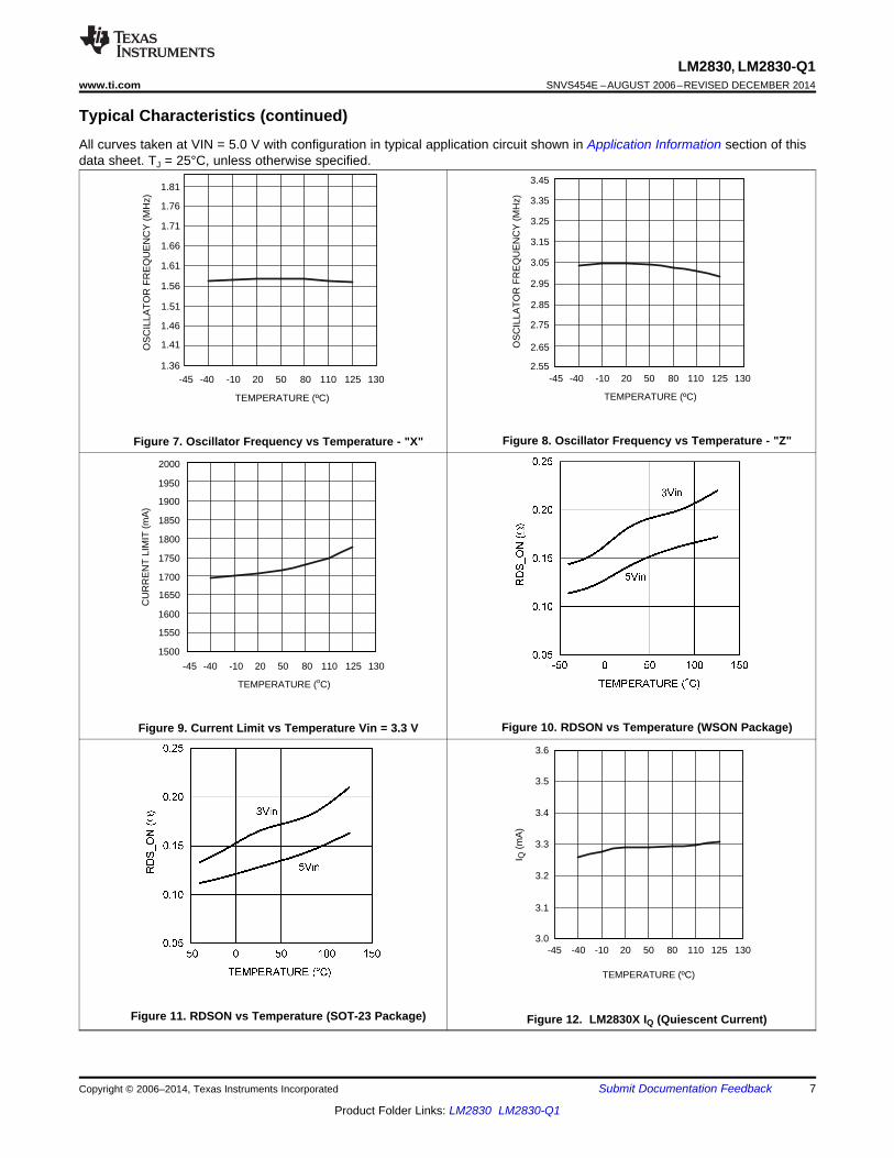
Typical Characteristics (continued)All curves taken at VIN = 5.0 V with configuration in typical application circuit shown in Application Information section of thisdata sheet. TJ = 25°C, unless otherwise specified.
Figure 8. Oscillator Frequency vs Temperature - "Z"Figure 7. Oscillator Frequency vs Temperature - "X"
Figure 10. RDSON vs Temperature (WSON Package)Figure 9. Current Limit vs Temperature Vin = 3.3 V
Figure 11. RDSON vs Temperature (SOT-23 Package) Figure 12. LM2830X IQ (Quiescent Current)
LM2830, LM2830-Q1SNVS454E –AUGUST 2006–REVISED DECEMBER 2014 www.ti.com
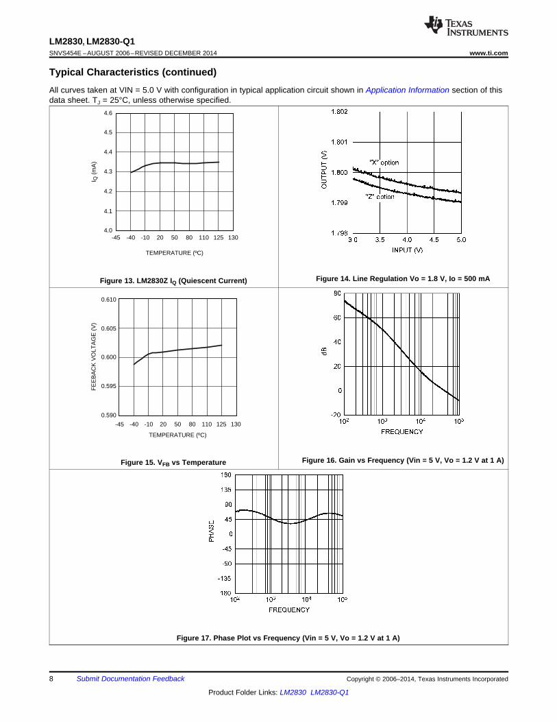
Typical Characteristics (continued)All curves taken at VIN = 5.0 V with configuration in typical application circuit shown in Application Information section of thisdata sheet. TJ = 25°C, unless otherwise specified.
Figure 14. Line Regulation Vo = 1.8 V, Io = 500 mAFigure 13. LM2830Z IQ (Quiescent Current)
Figure 16. Gain vs Frequency (Vin = 5 V, Vo = 1.2 V at 1 A)Figure 15. VFB vs Temperature
Figure 17. Phase Plot vs Frequency (Vin = 5 V, Vo = 1.2 V at 1 A)
LM2830, LM2830-Q1www.ti.com SNVS454E –AUGUST 2006–REVISED DECEMBER 2014
7 Detailed Description
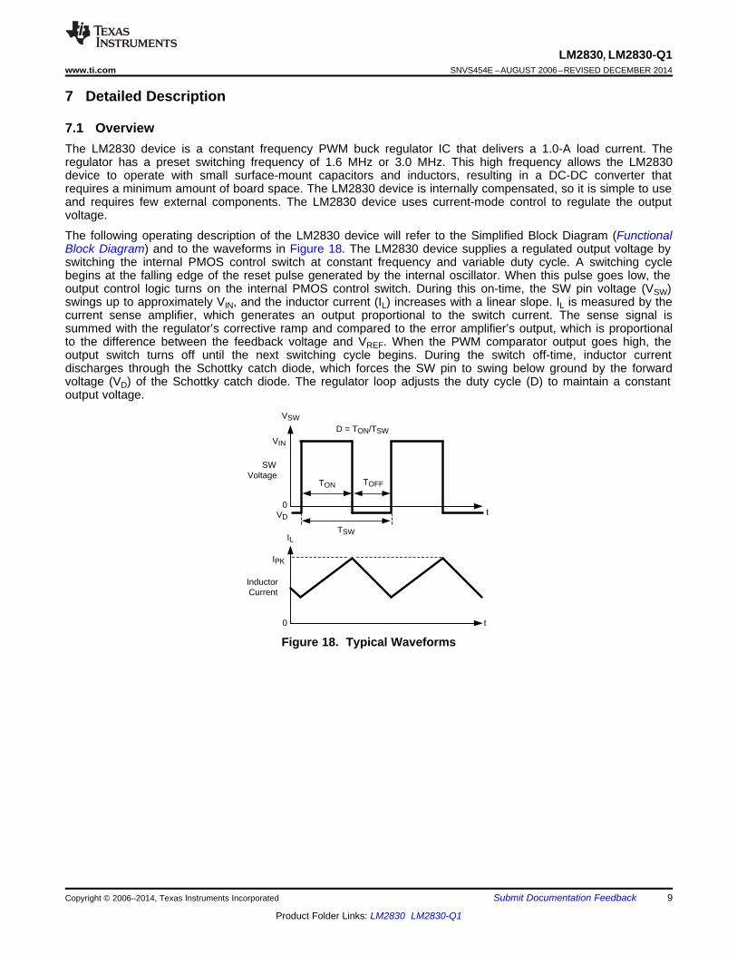
7.1 OverviewThe LM2830 device is a constant frequency PWM buck regulator IC that delivers a 1.0-A load current. Theregulator has a preset switching frequency of 1.6 MHz or 3.0 MHz. This high frequency allows the LM2830device to operate with small surface-mount capacitors and inductors, resulting in a DC-DC converter thatrequires a minimum amount of board space. The LM2830 device is internally compensated, so it is simple to useand requires few external components. The LM2830 device uses current-mode control to regulate the outputvoltage.
The following operating description of the LM2830 device will refer to the Simplified Block Diagram (FunctionalBlock Diagram) and to the waveforms in Figure 18. The LM2830 device supplies a regulated output voltage byswitching the internal PMOS control switch at constant frequency and variable duty cycle. A switching cyclebegins at the falling edge of the reset pulse generated by the internal oscillator. When this pulse goes low, theoutput control logic turns on the internal PMOS control switch. During this on-time, the SW pin voltage (VSW)swings up to approximately VIN, and the inductor current (IL) increases with a linear slope. IL is measured by thecurrent sense amplifier, which generates an output proportional to the switch current. The sense signal issummed with the regulator’s corrective ramp and compared to the error amplifier’s output, which is proportionalto the difference between the feedback voltage and VREF. When the PWM comparator output goes high, theoutput switch turns off until the next switching cycle begins. During the switch off-time, inductor currentdischarges through the Schottky catch diode, which forces the SW pin to swing below ground by the forwardvoltage (VD) of the Schottky catch diode. The regulator loop adjusts the duty cycle (D) to maintain a constantoutput voltage.
LM2830, LM2830-Q1SNVS454E –AUGUST 2006–REVISED DECEMBER 2014 www.ti.com
7.2 Functional Block Diagram
7.3 Feature Description
7.3.1 Soft-StartThis function forces VOUT to increase at a controlled rate during start up. During soft-start, the error referencevoltage of the amplifier ramps from 0 V to its nominal value of 0.6 V in approximately 600 µs. This forces theregulator output to ramp up in a controlled fashion, which helps reduce inrush current.
7.3.2 Output Overvoltage ProtectionThe overvoltage comparator compares the FB pin voltage to a voltage that is 15% higher than the internalreference VREF. Once the FB pin voltage goes 15% above the internal reference, the internal PMOS controlswitch is turned off, which allows the output voltage to decrease toward regulation.
7.3.3 Undervoltage LockoutUndervoltage lockout (UVLO) prevents the LM2830 device from operating until the input voltage exceeds 2.73 V(typical). The UVLO threshold has approximately 430 mV of hysteresis, so the part will operate until VIN dropsbelow 2.3V (typical). Hysteresis prevents the part from turning off during power up if VIN is nonmonotonic.
LM2830, LM2830-Q1www.ti.com SNVS454E –AUGUST 2006–REVISED DECEMBER 2014
Feature Description (continued)7.3.4 Current LimitThe LM2830 device uses cycle-by-cycle current limiting to protect the output switch. During each switching cycle,a current limit comparator detects if the output switch current exceeds 1.75 A (typical), and turns off the switchuntil the next switching cycle begins.
7.3.5 Thermal ShutdownThermal shutdown limits total power dissipation by turning off the output switch when the IC junction temperatureexceeds 165°C. After thermal shutdown occurs, the output switch does not turn on until the junction temperaturedrops to approximately 150°C.
7.4 Device Functional ModesIn normal operational mode, the device will regulate output voltage to the value set with resistive divider.
In addition, this device has an enable (EN) pin that lets the user turn the device on and off by driving this pin highand low. Default setup is that this pin is connected to VIN through pull up resistor (typically 100 kΩ). When enablepin is low the device is in shutdown mode consuming typically only 30 nA, making it ideal for applications wherelow power consumption is desirable.
LM2830, LM2830-Q1SNVS454E –AUGUST 2006–REVISED DECEMBER 2014 www.ti.com
8 Application and Implementation
NOTEInformation in the following applications sections is not part of the TI componentspecification, and TI does not warrant its accuracy or completeness. TI’s customers areresponsible for determining suitability of components for their purposes. Customers shouldvalidate and test their design implementation to confirm system functionality.
8.1 Application InformationThe device operates with input voltage in the range of 3.3 V to 5.5 V and provide regulated output voltage up to1 A of continuous DC load. This device is optimized for high efficiency operation with minimum number ofexternal components. Also, high switching frequency allows use of small surface-mount components enablingvery small solution size. For component selection, see Detailed Design Procedure.
8.2 Typical Applications
8.2.1 LM2830X Design Vo = 1.2 V at 1.0A
Figure 19. LM2830X (1.6 MHz): Vin = 5 V, Vo = 1.2 V at 1.0-A Schematic
8.2.1.1 Design RequirementsThis device must be able to operate at any voltage within input voltage range.
Load Current must be defined to properly size the inductor, input and output capacitors. Inductor should be ableto handle full expected load current as well as the peak current generated during load transients and start up.Inrush current at startup will depend on the output capacitor selection. More details are provided in DetailedDesign Procedure.
Device has an enable (EN) pin that is used to enable and disable the device. This pin is active high and shouldnot be left floating in application.
8.2.1.2 Detailed Design Procedure
Table 1. Bill of MaterialsPART ID PART VALUE MANUFACTURER PART NUMBER
U1 1.0-A Buck Regulator TI LM2830XC1, Input Cap 22 µF, 6.3 V, X5R TDK C3216X5ROJ226M
LM2830, LM2830-Q1www.ti.com SNVS454E –AUGUST 2006–REVISED DECEMBER 2014
Typical Applications (continued)Table 1. Bill of Materials (continued)
PART ID PART VALUE MANUFACTURER PART NUMBERL1 3.3 µH, 1.3 A Coilcraft ME3220-332R2 15.0 kΩ, 1% Vishay CRCW08051502FR1 15.0 kΩ, 1% Vishay CRCW08051502FR3 100 kΩ, 1% Vishay CRCW08051003F
8.2.1.2.1 Inductor Selection
The Duty Cycle (D) can be approximated quickly using the ratio of output voltage (VO) to input voltage (VIN):
(1)
The catch diode (D1) forward voltage drop and the voltage drop across the internal PMOS must be included tocalculate a more accurate duty cycle. Calculate D by using the following formula:
(2)
VSW can be approximated by:VSW = IOUT × RDSON (3)
The diode forward drop (VD) can range from 0.3 V to 0.7 V depending on the quality of the diode. The lower theVD, the higher the operating efficiency of the converter. The inductor value determines the output ripple current.Lower inductor values decrease the size of the inductor, but increase the output ripple current. An increase in theinductor value will decrease the output ripple current.
One must ensure that the minimum current limit (1.2 A) is not exceeded, so the peak current in the inductor mustbe calculated. The peak current (ILPK) in the inductor is calculated by:
ILPK = IOUT + ΔiL (4)
Figure 20. Inductor Current
(5)
In general,ΔiL = 0.1 × (IOUT) → 0.2 × (IOUT) (6)
If ΔiL = 20% of 1 A, the peak current in the inductor will be 1.2 A. The minimum ensured current limit over alloperating conditions is 1.2 A. One can either reduce ΔiL, or make the engineering judgment that zero margin willbe safe enough. The typical current limit is 1.75 A.
LM2830, LM2830-Q1SNVS454E –AUGUST 2006–REVISED DECEMBER 2014 www.ti.com
The LM2830 device operates at frequencies allowing the use of ceramic output capacitors without compromisingtransient response. Ceramic capacitors allow higher inductor ripple without significantly increasing output ripple.See the Output Capacitor for more details on calculating output voltage ripple. Now that the ripple current isdetermined, the inductance is calculated by:
where• Ts = 1/fs (7)
When selecting an inductor, make sure that it is capable of supporting the peak output current without saturating.Inductor saturation will result in a sudden reduction in inductance and prevent the regulator from operatingcorrectly. Because of the speed of the internal current limit, it is necessary to specify the peak current of theinductor only required maximum output current. For example, if the designed maximum output current is 1.0 Aand the peak current is 1.25 A, then the inductor should be specified with a saturation current limit of > 1.25 A.There is no need to specify the saturation or peak current of the inductor at the 1.75-A typical switch current limit.The difference in inductor size is a factor of 5. Because of the operating frequency of the LM2830 device, ferritebased inductors are preferred to minimize core losses. This presents little restriction because the variety offerrite-based inductors is huge. Lastly, inductors with lower series resistance (RDCR) will provide better operatingefficiency.
8.2.1.2.2 Input Capacitor
An input capacitor is necessary to ensure that VIN does not drop excessively during switching transients. Theprimary specifications of the input capacitor are capacitance, voltage, RMS current rating, and ESL (EquivalentSeries Inductance). The recommended input capacitance is 22 µF. The input voltage rating is specifically statedby the capacitor manufacturer. Make sure to check any recommended deratings and also verify if there is anysignificant change in capacitance at the operating input voltage and the operating temperature. The inputcapacitor maximum RMS input current rating (IRMS-IN) must be greater than:
(8)
Neglecting inductor ripple simplifies the above equation to:
(9)
From Equation 9, it can be shown that maximum RMS capacitor current occurs when D = 0.5. Always calculatethe RMS at the point where the duty cycle D is closest to 0.5. The ESL of an input capacitor is usuallydetermined by the effective cross sectional area of the current path. A large leaded capacitor will have high ESLand a 0805 ceramic chip capacitor will have very low ESL. At the operating frequencies of the LM2830 device,leaded capacitors may have an ESL so large that the resulting impedance (2πfL) will be higher than that requiredto provide stable operation. As a result, surface-mount capacitors are strongly recommended.
Sanyo POSCAP, Tantalum or Niobium, Panasonic SP, and multilayer ceramic capacitors (MLCC) are all goodchoices for both input and output capacitors and have very low ESL. For MLCCs it is recommended to use X7Ror X5R type capacitors due to their tolerance and temperature characteristics. Consult the capacitormanufacturer data sheets to see how rated capacitance varies over operating conditions.
8.2.1.2.3 Output Capacitor
The output capacitor is selected based upon the desired output ripple and transient response. The initial currentof a load transient is provided mainly by the output capacitor. The output ripple of the converter is:
(10)
When using MLCCs, the ESR is typically so low that the capacitive ripple may dominate. When this occurs, theoutput ripple will be approximately sinusoidal and 90° phase shifted from the switching action. Given theavailability and quality of MLCCs and the expected output voltage of designs using the LM2830 device, there isreally no need to review any other capacitor technologies. Another benefit of ceramic capacitors is their ability tobypass high frequency noise. A certain amount of switching edge noise will couple through parasitic
LM2830, LM2830-Q1www.ti.com SNVS454E –AUGUST 2006–REVISED DECEMBER 2014
capacitances in the inductor to the output. A ceramic capacitor will bypass this noise while a tantalum will not.Because the output capacitor is one of the two external components that control the stability of the regulatorcontrol loop, most applications will require a minimum of 22 µF of output capacitance. Capacitance often, but notalways, can be increased significantly with little detriment to the regulator stability. Like the input capacitor,recommended multilayer ceramic capacitors are X7R or X5R types.
8.2.1.2.4 Catch Diode
The catch diode (D1) conducts during the switch off-time. A Schottky diode is recommended for its fast switchingtimes and low forward voltage drop. The catch diode should be chosen so that its current rating is greater than:
ID1 = IOUT × (1-D) (11)
The reverse breakdown rating of the diode must be at least the maximum input voltage plus appropriate margin.To improve efficiency, choose a Schottky diode with a low forward voltage drop.
8.2.1.2.5 Output Voltage
The output voltage is set using Equation 12, where R2 is connected between the FB pin and GND, and R1 isconnected between VO and the FB pin. A good value for R2 is 10 kΩ. When designing a unity gain converter (Vo= 0.6 V), R1 should be between 0 Ω and 100 Ω, and R2 should be equal or greater than 10 kΩ.
(12)VREF = 0.60 V (13)
8.2.1.2.6 Calculating Efficiency, and Junction Temperature
The complete LM2830 DC-DC converter efficiency can be calculated in the following manner.
(14)
Or
(15)
Calculations for determining the most significant power losses are shown below. Other losses totaling less than2% are not discussed.
Power loss (PLOSS) is the sum of two basic types of losses in the converter: switching and conduction.Conduction losses usually dominate at higher output loads, whereas switching losses remain relatively fixed anddominate at lower output loads. The first step in determining the losses is to calculate the duty cycle (D):
(16)
VSW is the voltage drop across the internal PFET when it is on, and is equal to:VSW = IOUT × RDSON (17)
VD is the forward voltage drop across the Schottky catch diode. It can be obtained from the diode manufacturer'sElectrical Characteristics section. If the voltage drop across the inductor (VDCR) is accounted for, the equationbecomes:
(18)
The conduction losses in the free-wheeling Schottky diode are calculated as follows:PDIODE = VD × IOUT × (1-D) (19)
Often this is the single most significant power loss in the circuit. Care should be taken to choose a Schottkydiode that has a low forward voltage drop.
LM2830, LM2830-Q1SNVS454E –AUGUST 2006–REVISED DECEMBER 2014 www.ti.com
Another significant external power loss is the conduction loss in the output inductor. The equation can besimplified to:
PIND = IOUT2 × RDCR (20)
The conduction loss of the LC2830 device is mainly associated with the internal PFET:
(21)
If the inductor ripple current is fairly small, the conduction losses can be simplified to:PCOND = IOUT
2 × RDSON × D (22)
Switching losses are also associated with the internal PFET. They occur during the switch on and off transitionperiods, where voltages and currents overlap resulting in power loss. The simplest means to determine this lossis to empirically measuring the rise and fall times (10% to 90%) of the switch at the switch node.
Switching Power Loss is calculated as follows:PSWR = 1/2(VIN × IOUT × FSW × TRISE) (23)PSWF = 1/2(VIN × IOUT × FSW × TFALL) (24)PSW = PSWR + PSWF (25)
Another loss is the power required for operation of the internal circuitry:PQ = IQ × VIN (26)
IQ is the quiescent operating current, and is typically around 3.3 mA for the 1.6-MHz frequency option.
Table 2 lists typical application power losses.
Table 2. Power Loss TabulationDesign Parameter Value Design Parameter Value
VIN 5.0 VVOUT 3.3 V POUT 3.3 WIOUT 1.0AVD 0.45 V PDIODE 150 mW
LM2830, LM2830-Q1SNVS454E –AUGUST 2006–REVISED DECEMBER 2014 www.ti.com
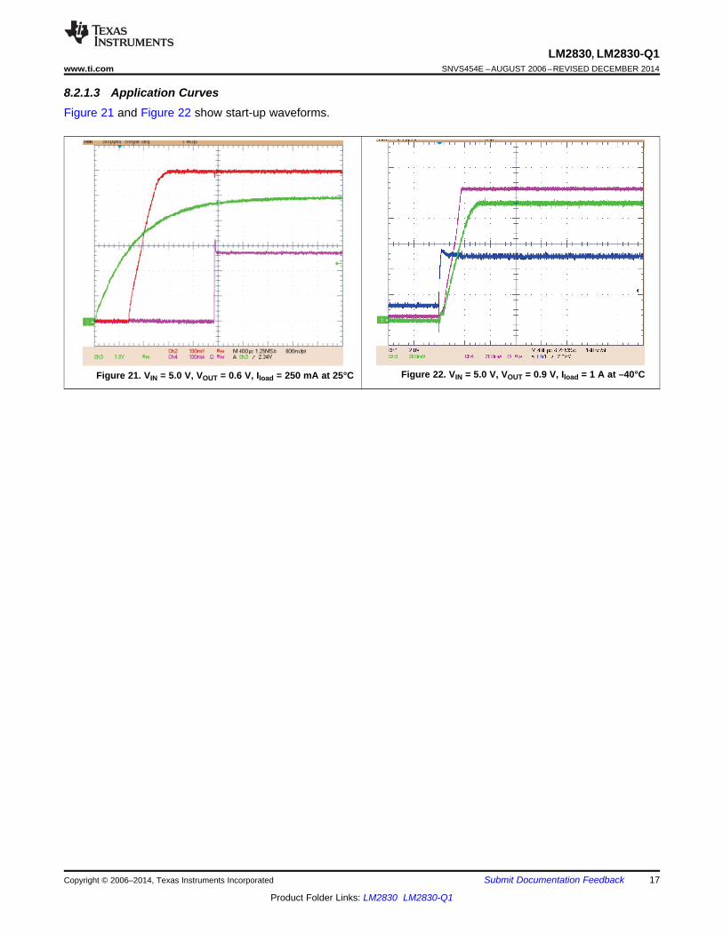
8.2.2 LM2830X Design Vo = 0.6 V at 1.0-AFigure 23 shows typical application circuit for step-down solution from VIN=5 to VOUT=0.6 V, 1.0-A load current.
Figure 23. LM2830X (1.6 MHz): Vin = 5 V, Vo = 0.6 V at 1.0-A Schematic
Table 3. Bill of MaterialsPART ID PART VALUE MANUFACTURER PART NUMBER
U1 1.0-A Buck Regulator TI LM2830XC1, Input Cap 22 µF, 6.3 V, X5R TDK C3216X5ROJ226M
LM2830, LM2830-Q1www.ti.com SNVS454E –AUGUST 2006–REVISED DECEMBER 2014
8.2.3 LM2830X Design Vo = 3.3 V at 1.0-AFigure 24 shows typical application circuit for step down solution from VIN=5 to VOUT=3.3 V, 1.0-A load current.
Figure 24. LM2830X (1.6 MHz): Vin = 5 V, Vo = 3.3 V at 1.0-A Schematic
Table 4. Bill of MaterialsPART ID PART VALUE MANUFACTURER PART NUMBER
U1 1.0-A Buck Regulator TI LM2830XC1, Input Cap 22 µF, 6.3 V, X5R TDK C3216X5ROJ226M
LM2830, LM2830-Q1SNVS454E –AUGUST 2006–REVISED DECEMBER 2014 www.ti.com
8.2.4 LM2830Z Design Vo = 3.3 V at 1.0-AFigure 25 shows typical application circuit for step down solution from VIN=5 to VOUT=3.3 V, 1.0-A load currentwhen using device version with higher switching frequency.
Figure 25. LM2830Z (3 MHz): Vin = 5 V, Vo = 3.3 V at 1.0-A Schematic
Table 5. Bill of MaterialsPART ID PART VALUE MANUFACTURER PART NUMBER
U1 1.0-A Buck Regulator TI LM2830ZC1, Input Cap 22 µF, 6.3 V, X5R TDK C3216X5ROJ226M
C2, Output Cap 22 µF, 6.3 V, X5R TDK C3216X5ROJ226MD1, Catch Diode 0.3 Vf Schottky 1.5 A, 30VR TOSHIBA CRS08
LM2830, LM2830-Q1www.ti.com SNVS454E –AUGUST 2006–REVISED DECEMBER 2014
8.2.5 LM2830Z Design Vo = 1.2 V at 1.0-AFigure 26 shows a typical application circuit for step down solution from VIN=5 to VOUT=1.2 V, 1.0-A load currentwhen using device version with higher switching frequency.
Figure 26. LM2830Z (3 MHz): Vin = 5 V, Vo = 1.2 V at 1.0-A Schematic
Table 6. Bill of MaterialsPART ID PART VALUE MANUFACTURER PART NUMBER
U1 1.0-A Buck Regulator TI LM2830ZC1, Input Cap 22 µF, 6.3 V, X5R TDK C3216X5ROJ226M
C2, Output Cap 22 µF, 6.3 V, X5R TDK C3216X5ROJ226MD1, Catch Diode 0.3Vf Schottky 1.5 A, 30VR TOSHIBA CRS08
LM2830, LM2830-Q1SNVS454E –AUGUST 2006–REVISED DECEMBER 2014 www.ti.com
8.2.6 LM2830X Dual Converters With Delayed Enabled DesignFigure 27 shows proposed solution with two LM2830 devices. Output of device on top (3.3-V output) is used tocontrol the enable pin of the lower device, thus ensuring that the second device (1.2-V output) can not turn onbefore the output of first device (3.3-V in this example) reaches steady state. Additionally, small POR supervisory(LP3470) circuit is used to monitor enable voltage for lower device. The RESET pin on POR circuit is open drainand requires typically 20-kΩ pullup resistor to the monitored voltage.
Figure 27. LM2830X (1.6 MHz): Vin = 5 V, Vo = 1.2 V at 1.0 A and 3.3 V at 1.0-A Schematic
Table 7. Bill of MaterialsPART ID PART VALUE MANUFACTURER PART NUMBERU1, U2 1.0-A Buck Regulator TI LM2830X
U3 Power on Reset TI LP3470M5X-3.08C1, C3 Input Cap 22 µF, 6.3 V, X5R TDK C3216X5ROJ226M
LM2830, LM2830-Q1www.ti.com SNVS454E –AUGUST 2006–REVISED DECEMBER 2014
8.2.7 LM2830X Buck Converter and Voltage Double Circuit With LDO FollowerFigure 28 shows an example where the LM2830 device is used to provide regulated output voltage (3.3 V) aswell as input voltage for an LDO, effectively providing solution with two output voltages.
Figure 28. LM2830X (1.6 MHz): Vin = 5 V, Vo = 3.3 V at 1.0 A and LP2986-5.0 at 150-mA Schematic
Table 8. Bill of MaterialsPART ID PART VALUE MANUFACTURER PART NUMBER
U1 1.0-A Buck Regulator TI LM2830XU2 200-mA LDO TI LP2986-5.0
C1, Input Cap 22 µF, 6.3 V, X5R TDK C3216X5ROJ226MC2, Output Cap 22 µF, 6.3 V, X5R TDK C3216X5ROJ226M
LM2830, LM2830-Q1SNVS454E –AUGUST 2006–REVISED DECEMBER 2014 www.ti.com
9 Power Supply RecommendationsThe LM2830 is designed to operate from an input voltage supply range between 3.0 V and 5.5 V. This inputsupply should be able to withstand the maximum input current and maintain a voltage above 3.0 V. If the inputsupply is located farther away (more than a few inches) from the LM2830, additional bulk capacitance may berequired in addition to the ceramic bypass capacitors.
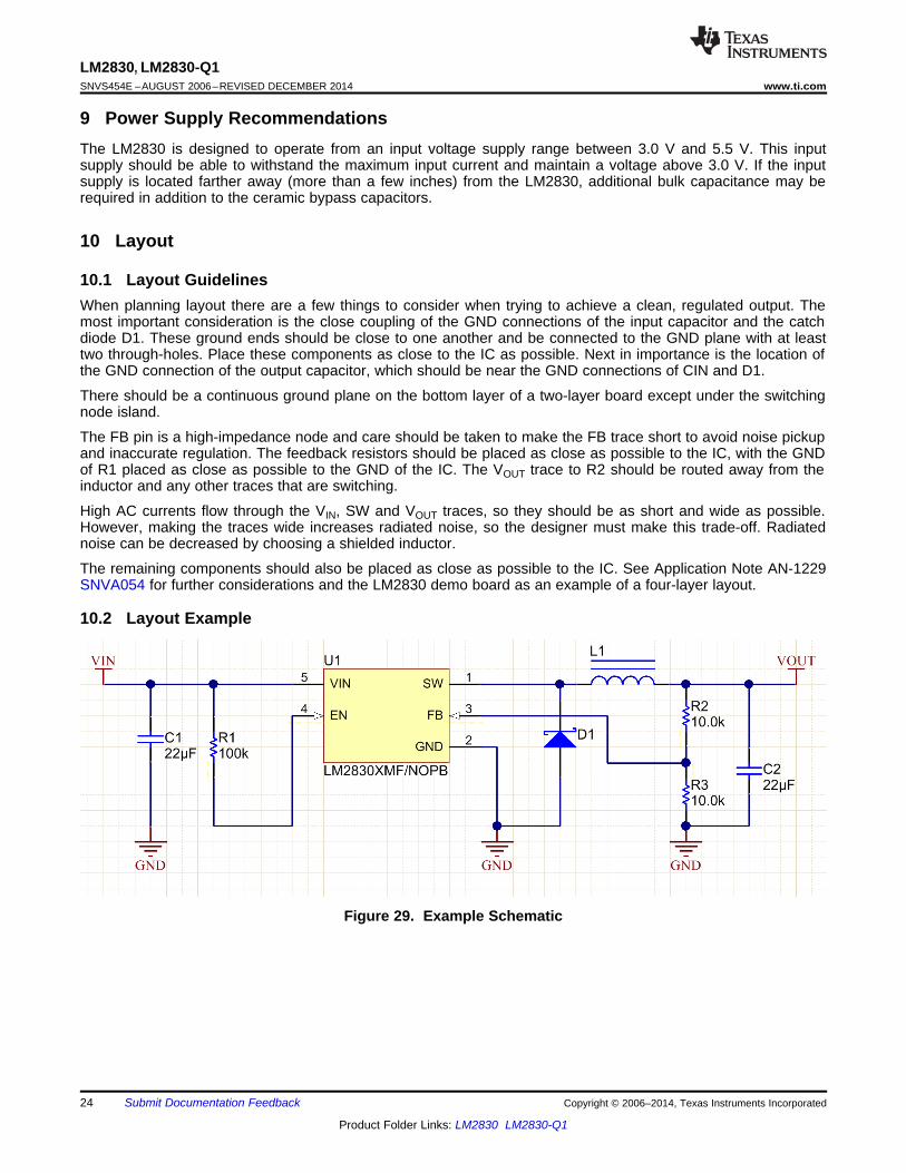
10 Layout
10.1 Layout GuidelinesWhen planning layout there are a few things to consider when trying to achieve a clean, regulated output. Themost important consideration is the close coupling of the GND connections of the input capacitor and the catchdiode D1. These ground ends should be close to one another and be connected to the GND plane with at leasttwo through-holes. Place these components as close to the IC as possible. Next in importance is the location ofthe GND connection of the output capacitor, which should be near the GND connections of CIN and D1.
There should be a continuous ground plane on the bottom layer of a two-layer board except under the switchingnode island.
The FB pin is a high-impedance node and care should be taken to make the FB trace short to avoid noise pickupand inaccurate regulation. The feedback resistors should be placed as close as possible to the IC, with the GNDof R1 placed as close as possible to the GND of the IC. The VOUT trace to R2 should be routed away from theinductor and any other traces that are switching.
High AC currents flow through the VIN, SW and VOUT traces, so they should be as short and wide as possible.However, making the traces wide increases radiated noise, so the designer must make this trade-off. Radiatednoise can be decreased by choosing a shielded inductor.
The remaining components should also be placed as close as possible to the IC. See Application Note AN-1229SNVA054 for further considerations and the LM2830 demo board as an example of a four-layer layout.
LM2830, LM2830-Q1www.ti.com SNVS454E –AUGUST 2006–REVISED DECEMBER 2014
Layout Example (continued)
Figure 30. PCB Layout Example
10.3 Thermal ConsiderationsThe PCB size, weight of copper used to route traces and ground plane, and number of layers within the PCB cangreatly effect RθJA. The type and number of thermal vias can also make a large difference in the thermalimpedance. Thermal vias are necessary in most applications. They conduct heat from the surface of the PCB tothe ground plane. Four to six thermal vias should be placed under the exposed pad to the ground plane if theWSON package is used.
Thermal impedance also depends on the thermal properties of the application operating conditions (Vin, Vo, Ioetc), and the surrounding circuitry.
Silicon Junction Temperature Determination Method 1:To accurately measure the silicon temperature for a given application, two methods can be used. The firstmethod requires the user to know the thermal impedance of the silicon junction to top case temperature.
Some clarification needs to be made before we go any further.
RθJC is the thermal impedance from all six sides of an IC package to silicon junction.
RΦJC is the thermal impedance from top case to the silicon junction.
In this data sheet we will use RΦJC so that it allows the user to measure top case temperature with a smallthermocouple attached to the top case.
LM2830, LM2830-Q1SNVS454E –AUGUST 2006–REVISED DECEMBER 2014 www.ti.com
Thermal Considerations (continued)RΦJC is approximately 30°C/Watt for the 6-pin WSON package with the exposed pad. Knowing the internaldissipation from the efficiency calculation given previously, and the case temperature, which can be empiricallymeasured on the bench we have:
(30)
Therefore:Tj = (RΦJC x PLOSS) + TC (31)
From the previous example:Tj = (RΦJC x PINTERNAL) + TC (32)Tj = 30°C/W x 0.189W + TC (33)
The second method can give a very accurate silicon junction temperature.
The first step is to determine RθJA of the application. The LM2830 device has over-temperature protectioncircuitry. When the silicon temperature reaches 165°C, the device stops switching. The protection circuitry has ahysteresis of about 15°C. Once the silicon temperature has decreased to approximately 150°C, the device willstart to switch again. Knowing this, the RθJA for any application can be characterized during the early stages ofthe design one may calculate the RθJA by placing the PCB circuit into a thermal chamber. Raise the ambienttemperature in the given working application until the circuit enters thermal shutdown. If the SW-pin is monitored,it will be obvious when the internal PFET stops switching, indicating a junction temperature of 165°C. Knowingthe internal power dissipation from the above methods, the junction temperature, and the ambient temperatureRθJA can be determined.
(34)
Once this is determined, the maximum ambient temperature allowed for a desired junction temperature can befound.
An example of calculating RθJA for an application using the Texas Instruments LM2830 WSON demonstrationboard is shown below.
The four layer PCB is constructed using FR4 with ½ oz copper traces. The copper ground plane is on the bottomlayer. The ground plane is accessed by two vias. The board measures 3-cm × 3-cm. It was placed in an ovenwith no forced airflow. The ambient temperature was raised to 144°C, and at that temperature, the device wentinto thermal shutdown.
From the previous example:PINTERNAL = 189mW (35)
(36)
If the junction temperature was to be kept below 125°C, then the ambient temperature could not go above 109°CTj - (RθJA x PLOSS) = TA (37)125°C - (111°C/W x 189mW) = 104°C (38)
LM2830, LM2830-Q1www.ti.com SNVS454E –AUGUST 2006–REVISED DECEMBER 2014
10.4 WSON Package
Figure 31. Internal WSON Connection
For certain high-power applications, the PCB land may be modified to a "dog bone" shape (see Figure 32). Byincreasing the size of ground plane, and adding thermal vias, the RθJA for the application can be reduced.
LM2830, LM2830-Q1SNVS454E –AUGUST 2006–REVISED DECEMBER 2014 www.ti.com
11 Device and Documentation Support
11.1 Device Support
11.1.1 Third-Party Products DisclaimerTI'S PUBLICATION OF INFORMATION REGARDING THIRD-PARTY PRODUCTS OR SERVICES DOES NOTCONSTITUTE AN ENDORSEMENT REGARDING THE SUITABILITY OF SUCH PRODUCTS OR SERVICESOR A WARRANTY, REPRESENTATION OR ENDORSEMENT OF SUCH PRODUCTS OR SERVICES, EITHERALONE OR IN COMBINATION WITH ANY TI PRODUCT OR SERVICE.
11.1.2 Thermal DefinitionsTJ Chip junction temperature
TA Ambient temperature
RθJC Thermal resistance from chip junction to device case
RθJA Thermal resistance from chip junction to ambient air
Heat in the LM2830 device due to internal power dissipation is removed through conduction and/or convection.
Conduction: Heat transfer occurs through cross sectional areas of material. Depending on the material, thetransfer of heat can be considered to have poor to good thermal conductivity properties (insulatorvs. conductor).
Heat Transfer goes as:
Silicon → package → lead frame → PCB
Convection: Heat transfer is by means of airflow. This could be from a fan or natural convection. Naturalconvection occurs when air currents rise from the hot device to cooler air.
Thermal impedance is defined as:
(39)
Thermal impedance from the silicon junction to the ambient air is defined as:
(40)
11.2 Related LinksThe table below lists quick access links. Categories include technical documents, support and communityresources, tools and software, and quick access to sample or buy.
Table 9. Related LinksTECHNICAL TOOLS & SUPPORT &PARTS PRODUCT FOLDER SAMPLE & BUY DOCUMENTS SOFTWARE COMMUNITY
LM2830 Click here Click here Click here Click here Click hereLM2830-Q1 Click here Click here Click here Click here Click here
11.3 TrademarksAll trademarks are the property of their respective owners.
11.4 Electrostatic Discharge CautionThese devices have limited built-in ESD protection. The leads should be shorted together or the device placed in conductive foamduring storage or handling to prevent electrostatic damage to the MOS gates.
LM2830, LM2830-Q1www.ti.com SNVS454E –AUGUST 2006–REVISED DECEMBER 2014
11.5 GlossarySLYZ022 — TI Glossary.
This glossary lists and explains terms, acronyms, and definitions.
12 Mechanical, Packaging, and Orderable InformationThe following pages include mechanical, packaging, and orderable information. This information is the mostcurrent data available for the designated devices. This data is subject to change without notice and revision ofthis document. For browser-based versions of this data sheet, refer to the left-hand navigation.
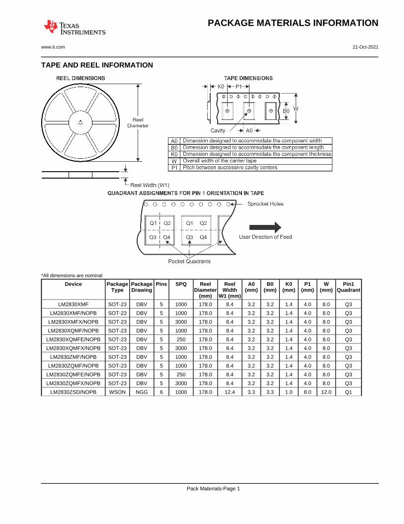
LM2830XMF/NOPB ACTIVE SOT-23 DBV 5 1000 RoHS & Green SN Level-1-260C-UNLIM -40 to 125 SKTB
LM2830XMFX/NOPB ACTIVE SOT-23 DBV 5 3000 RoHS & Green SN Level-1-260C-UNLIM -40 to 125 SKTB
LM2830XQMF/NOPB ACTIVE SOT-23 DBV 5 1000 RoHS & Green SN Level-1-260C-UNLIM -40 to 125 SUFB
LM2830XQMFE/NOPB ACTIVE SOT-23 DBV 5 250 RoHS & Green SN Level-1-260C-UNLIM -40 to 125 SUFB
LM2830XQMFX/NOPB ACTIVE SOT-23 DBV 5 3000 RoHS & Green SN Level-1-260C-UNLIM -40 to 125 SUFB
LM2830ZMF/NOPB ACTIVE SOT-23 DBV 5 1000 RoHS & Green SN Level-1-260C-UNLIM -40 to 125 SKXB
LM2830ZQMF/NOPB ACTIVE SOT-23 DBV 5 1000 RoHS & Green SN Level-1-260C-UNLIM -40 to 125 SURB
LM2830ZQMFE/NOPB ACTIVE SOT-23 DBV 5 250 RoHS & Green SN Level-1-260C-UNLIM -40 to 125 SURB
LM2830ZQMFX/NOPB ACTIVE SOT-23 DBV 5 3000 RoHS & Green SN Level-1-260C-UNLIM -40 to 125 SURB
LM2830ZSD/NOPB ACTIVE WSON NGG 6 1000 RoHS & Green SN Level-3-260C-168 HR -40 to 125 L192B
(1) The marketing status values are defined as follows:ACTIVE: Product device recommended for new designs.LIFEBUY: TI has announced that the device will be discontinued, and a lifetime-buy period is in effect.NRND: Not recommended for new designs. Device is in production to support existing customers, but TI does not recommend using this part in a new design.PREVIEW: Device has been announced but is not in production. Samples may or may not be available.OBSOLETE: TI has discontinued the production of the device.
(2) RoHS: TI defines "RoHS" to mean semiconductor products that are compliant with the current EU RoHS requirements for all 10 RoHS substances, including the requirement that RoHS substancedo not exceed 0.1% by weight in homogeneous materials. Where designed to be soldered at high temperatures, "RoHS" products are suitable for use in specified lead-free processes. TI mayreference these types of products as "Pb-Free".RoHS Exempt: TI defines "RoHS Exempt" to mean products that contain lead but are compliant with EU RoHS pursuant to a specific EU RoHS exemption.Green: TI defines "Green" to mean the content of Chlorine (Cl) and Bromine (Br) based flame retardants meet JS709B low halogen requirements of <=1000ppm threshold. Antimony trioxide basedflame retardants must also meet the <=1000ppm threshold requirement.
(3) MSL, Peak Temp. - The Moisture Sensitivity Level rating according to the JEDEC industry standard classifications, and peak solder temperature.
(4) There may be additional marking, which relates to the logo, the lot trace code information, or the environmental category on the device.
(5) Multiple Device Markings will be inside parentheses. Only one Device Marking contained in parentheses and separated by a "~" will appear on a device. If a line is indented then it is a continuationof the previous line and the two combined represent the entire Device Marking for that device.
(6) Lead finish/Ball material - Orderable Devices may have multiple material finish options. Finish options are separated by a vertical ruled line. Lead finish/Ball material values may wrap to twolines if the finish value exceeds the maximum column width.
Important Information and Disclaimer:The information provided on this page represents TI's knowledge and belief as of the date that it is provided. TI bases its knowledge and belief on informationprovided by third parties, and makes no representation or warranty as to the accuracy of such information. Efforts are underway to better integrate information from third parties. TI has taken andcontinues to take reasonable steps to provide representative and accurate information but may not have conducted destructive testing or chemical analysis on incoming materials and chemicals.TI and TI suppliers consider certain information to be proprietary, and thus CAS numbers and other limited information may not be available for release.
In no event shall TI's liability arising out of such information exceed the total purchase price of the TI part(s) at issue in this document sold by TI to Customer on an annual basis.
OTHER QUALIFIED VERSIONS OF LM2830, LM2830-Q1 :
• Catalog : LM2830
• Automotive : LM2830-Q1
NOTE: Qualified Version Definitions:
• Catalog - TI's standard catalog product
• Automotive - Q100 devices qualified for high-reliability automotive applications targeting zero defects
SOT-23 - 1.45 mm max heightDBV0005ASMALL OUTLINE TRANSISTOR
4214839/F 06/2021
NOTES: 1. All linear dimensions are in millimeters. Any dimensions in parenthesis are for reference only. Dimensioning and tolerancing per ASME Y14.5M.2. This drawing is subject to change without notice.3. Refernce JEDEC MO-178.4. Body dimensions do not include mold flash, protrusions, or gate burrs. Mold flash, protrusions, or gate burrs shall not exceed 0.25 mm per side.
0.2 C A B
1
34
5
2
INDEX AREAPIN 1
GAGE PLANE
SEATING PLANE
0.1 C
SCALE 4.000
www.ti.com
EXAMPLE BOARD LAYOUT
0.07 MAXARROUND
0.07 MINARROUND
5X (1.1)
5X (0.6)
(2.6)
(1.9)
2X (0.95)
(R0.05) TYP
4214839/F 06/2021
SOT-23 - 1.45 mm max heightDBV0005ASMALL OUTLINE TRANSISTOR
NOTES: (continued) 5. Publication IPC-7351 may have alternate designs. 6. Solder mask tolerances between and around signal pads can vary based on board fabrication site.
SYMM
LAND PATTERN EXAMPLEEXPOSED METAL SHOWN
SCALE:15X
PKG
1
3 4
5
2
SOLDER MASKOPENINGMETAL UNDER
SOLDER MASK
SOLDER MASKDEFINED
EXPOSED METAL
METALSOLDER MASKOPENING
NON SOLDER MASKDEFINED
(PREFERRED)
SOLDER MASK DETAILS
EXPOSED METAL
www.ti.com
EXAMPLE STENCIL DESIGN
(2.6)
(1.9)
2X(0.95)
5X (1.1)
5X (0.6)
(R0.05) TYP
SOT-23 - 1.45 mm max heightDBV0005ASMALL OUTLINE TRANSISTOR
4214839/F 06/2021
NOTES: (continued) 7. Laser cutting apertures with trapezoidal walls and rounded corners may offer better paste release. IPC-7525 may have alternate design recommendations. 8. Board assembly site may have different recommendations for stencil design.
SOLDER PASTE EXAMPLEBASED ON 0.125 mm THICK STENCIL
SCALE:15X
SYMM
PKG
1
3 4
5
2
MECHANICAL DATA
NGG0006A
www.ti.com
SDE06A (Rev A)
IMPORTANT NOTICE AND DISCLAIMERTI PROVIDES TECHNICAL AND RELIABILITY DATA (INCLUDING DATA SHEETS), DESIGN RESOURCES (INCLUDING REFERENCE DESIGNS), APPLICATION OR OTHER DESIGN ADVICE, WEB TOOLS, SAFETY INFORMATION, AND OTHER RESOURCES “AS IS” AND WITH ALL FAULTS, AND DISCLAIMS ALL WARRANTIES, EXPRESS AND IMPLIED, INCLUDING WITHOUT LIMITATION ANY IMPLIED WARRANTIES OF MERCHANTABILITY, FITNESS FOR A PARTICULAR PURPOSE OR NON-INFRINGEMENT OF THIRD PARTY INTELLECTUAL PROPERTY RIGHTS.These resources are intended for skilled developers designing with TI products. You are solely responsible for (1) selecting the appropriate TI products for your application, (2) designing, validating and testing your application, and (3) ensuring your application meets applicable standards, and any other safety, security, regulatory or other requirements.These resources are subject to change without notice. TI grants you permission to use these resources only for development of an application that uses the TI products described in the resource. Other reproduction and display of these resources is prohibited. No license is granted to any other TI intellectual property right or to any third party intellectual property right. TI disclaims responsibility for, and you will fully indemnify TI and its representatives against, any claims, damages, costs, losses, and liabilities arising out of your use of these resources.TI’s products are provided subject to TI’s Terms of Sale or other applicable terms available either on ti.com or provided in conjunction with such TI products. TI’s provision of these resources does not expand or otherwise alter TI’s applicable warranties or warranty disclaimers for TI products.TI objects to and rejects any additional or different terms you may have proposed. IMPORTANT NOTICE