www.ti.com SNVS626B –NOVEMBER 2009–REVISED MARCH 2013
LM3209-G3 Seamless-Transition Buck-Boost Converter for Battery-Powered 3G/4G RFPower Amplifiers
Check for Samples: LM3209-G3
1FEATURES APPLICATIONS2• Operates From a Single Li-Ion Cell: 2.7V to • Battery-Powered 3G/4G RF PAs
5.5V • Cellular Phones• Adjustable Output Voltage: 0.6V to 4.2V • Portable Hard Disk Drives• 1A Maximum Load Capability for VIN ≥ 3.2V, • PDAs
VOUT = 3.6V• 2.4 MHz (typ.) Switching Frequency DESCRIPTION
The LM3209-G3 is buck-boost DC/DC converter• Seamless Buck-Boost Mode Transitiondesigned to generate output voltages above or below• Fast Output Voltage Transition: 0.8V to 4.0V ina given input voltage. It is particularly suitable for20 µs single-cell Li-ion batteries for portable applications.
• High-Efficiency: 95% typ. at 3.7 VIN, 3.5 VOUT, atThe LM3209-G3 operates at a 2.4 MHz typical300 mAswitching frequency in full synchronous operation
• Cycle-by-cycle Over-Current Limit providing seamless transitions between buck and• Output Over-Voltage Clamp boost operating modes.• Internal Compensation The power converter topology needs only one
external inductor and two capacitors. Five internal• 12-bump DSBGA Packagepower switches enable high overall efficiency.
The LM3209-G3 is internally compensated for buckand boost modes of operation, thus providing anoptimal transient response.
The LM3209-G3 is available in an 12-bump lead-freeDSBGA package of size 2.0 mm x 2.5 mm x 0.6 mm.
TYPICAL APPLICATION CIRCUIT
1
Please be aware that an important notice concerning availability, standard warranty, and use in critical applications ofTexas Instruments semiconductor products and disclaimers thereto appears at the end of this data sheet.
2All trademarks are the property of their respective owners.
SNVS626B –NOVEMBER 2009–REVISED MARCH 2013 www.ti.com
CONNECTION DIAGRAMS AND PACKAGE MARK INFORMATION
Figure 1. 12–Bump Thin DSBGA Package, Large Bump
PIN DESCRIPTIONSPin # Name Description
A1 NC This pin is shorted to ground internally. Leave this pin floating.
B1 VCON Output voltage program pin. Analog voltage from DAC/controller to set VOUT.
C1 FB Feedback input to inverting input of error amplifier. Connect output voltage directly to this nodeat load point.
D1 VOUT Regulated output voltage of LM3209-G3. Connect this to a 4.7 µF ceramic output filtercapacitor to GND.
A2 NC Supply voltage for analog circuits of LM3209-G3. This pin is connected to PVIN via a 36Ωresistor internally. Leave this pin floating.
B2 EN Enable Pin. Pulling this pin higher than 1.2V enables part to function.
C2 SGND Signal Ground for analog circuits.
D2 SW2 Switch pin for Internal Power Switches M3 and M4. Connect inductor between SW1 and SW2.
A3 PVIN Power MOSFET input and power current input pin. Optional low-pass filtering may help buckand buck-boost modes for radiated EMI and noise reduction.
B3 PVIN Power MOSFET input and power current input pin. Optional low-pass filtering may help buckand buck-boost modes for radiated EMI and noise reduction.
C3 SW1 Switch pin for Internal Power Switches M1 and M2. Connect inductor between SW1 and SW2.
D3 PGND Power Ground for Power MOSFETs and gate drive circuitry.
This integrated circuit can be damaged by ESD. Texas Instruments recommends that all integrated circuits be handled withappropriate precautions. Failure to observe proper handling and installation procedures can cause damage.
ESD damage can range from subtle performance degradation to complete device failure. Precision integrated circuits may be moresusceptible to damage because very small parametric changes could cause the device not to meet its published specifications.
www.ti.com SNVS626B –NOVEMBER 2009–REVISED MARCH 2013
ABSOLUTE MAXIMUM RATINGS (1) (2) (3)
PVIN pin: Voltage to GND −0.2V to +6.0V
EN, FB, VCON, VOUT pin: Voltage to GND −0.2V) to (VIN +0.2V) w/6.0Vmax.
PGND to SGND −0.2V to +0.2V
SW1, SW2 (PGND −0.2V)to (PVIN +0.2V) w/6.0V
Continuous Power Dissipation (4) Internally Limited
Junction Temperature (TJ-MAX) +150°C
Storage Temperature Range −65°C to +150°C
Maximum Lead Temperature (Soldering 10 sec.) +260°C
ESD Rating, Human Body Model (5) (6) 2kV
(1) Stresses beyond those listed under absolute maximum ratings may cause permanent damage to the device. These are stress ratingsonly, and functional operation of the device at these or any other conditions beyond those indicated under recommended operatingconditions is not implied. Exposure to absolute-maximum-rated conditions for extended periods may affect device reliability.
(2) All voltages are with respect to the potential at the GND pins.(3) If Military/Aerospace specified devices are required, please contact the Texas Instruments Sales Office/Distributors for availability and
specifications.(4) Internal thermal shutdown circuitry protects the device from permanent damage. Thermal shutdown engages at TJ = 150°C (typ.) and
disengages at TJ = 120°C (typ.).(5) The Human body model is a 100 pF capacitor discharged through a 1.5 kΩ resistor into each pin. (MIL-STD-883 3015.7)(6) Texas Instruments recommends that all integrated circuits be handled with appropriate precautions. Failure to observe proper ESD
handling procedure can result in damage.
OPERATING RATINGS (1) (2)
Input Voltage Range 2.7V to 5.5V
Recommended Load Current 0 to 650 mA
Junction Temperature (TJ) Range −30°C to +125°C
Ambient Temperature (TA) Range (3) −30°C to +85°C
(1) Stresses beyond those listed under absolute maximum ratings may cause permanent damage to the device. These are stress ratingsonly, and functional operation of the device at these or any other conditions beyond those indicated under recommended operatingconditions is not implied. Exposure to absolute-maximum-rated conditions for extended periods may affect device reliability.
(2) All voltages are with respect to the potential at the GND pins.(3) In applications where high power dissipation and/or poor package thermal resistance is present, the maximum ambient temperature may
have to be de-rated. Maximum ambient temperature (TA-MAX) is dependent on the maximum operating junction temperature (TJ-MAX-OP =125°C), the maximum power dissipation of the device in the application (PD-MAX), and the junction-to ambient thermal resistance of thepart/package in the application (θJA), as given by the following equation: TA-MAX = TJ-MAX-OP – (θJA × PD-MAX).
SNVS626B –NOVEMBER 2009–REVISED MARCH 2013 www.ti.com
ELECTRICAL CHARACTERISTICS (1) (2)
Limits in standard typeface are for TA = TJ = 25°C. Limits in boldface type apply over the full operating ambient temperaturerange (−30°C ≤ TJ = TA ≤ +85°C). Unless otherwise noted, specifications apply to the LM3209-G3 Typical Application Circuitwith: PVIN = EN = 3.6V.
Symbol Parameter Conditions Min Typ Max Units
VFB, min Min FB voltage VCON = 0.2V 0.530 0.600 0.670 V
VFB, max Max FB voltage VCON = 1.4V 4.130 4.200 4.270 V
No switching (3),IQ Quiescent current 0.8 2.0 mAVCON = 0.1V, FB = PVIN
EN = 0V, VCON = 0V,ISHDN Shutdown supply current 0.02 2 µASW1 = SW2 = VOUT = 0V
RDSON Buck PMOS switch on resistance M1, ISW1 = 200 mA 415 mΩPMOS (Small PFET)
RDSON Buck PMOS switch on resistance 140M1, ISW1 = 200 mA 120 mΩPMOS (Large+Small PFET) 165
RDSON Buck PMOS switch on resistance 90M1, ISW1 = 200 mA 80 mΩPMOS during boost operation 110
RDSON Buck and Boost NMOS switch on M2, ISW1 = -200 mA 230215 mΩNMOS resistance M4, ISW2 = −200 mA 285
NMOS output switch onRDSON M5, ISW2 = 200 mA 110resistance (between SW2 and 100 mΩNMOS VOUT = 0.8V 135VOUT)
ILIM_L Input Current Limit (Large) Open Loop (4) 1500 1700 1900 mA
ILIM_S Input Current Limit (Small) Open Loop (4) 750 850 mA
ISHRT Output Short Current FB ≤ 0.35V 850 mA
FOSC Internal Oscillator Frequency 2.1 2.4 2.7 MHz
Gain Internal Gain (5) 0.2V ≤ VCON ≤ 1.4V 3 V/V
IEN EN pin pull down current 5 10 µA
ICON VCON pin input current 0.02 2 µA
VIH Logic High Input Threshold for EN 1.2 V
VIL Logic Low Input Threshold for EN 0.6 V
(1) All voltages are with respect to the potential at the GND pins.(2) Min and Max limits are verified by design, test, or statistical analysis.(3) IQ specified here is when the part is not switching.(4) Current limit is built-in, fixed, and not adjustable.(5) To calculate VOUT, use the following equation: VOUT = VCON × 3
Dissipation Rating TableAmbient Temperature TA = 25°C TA = 55°C TA = 85°C
www.ti.com SNVS626B –NOVEMBER 2009–REVISED MARCH 2013
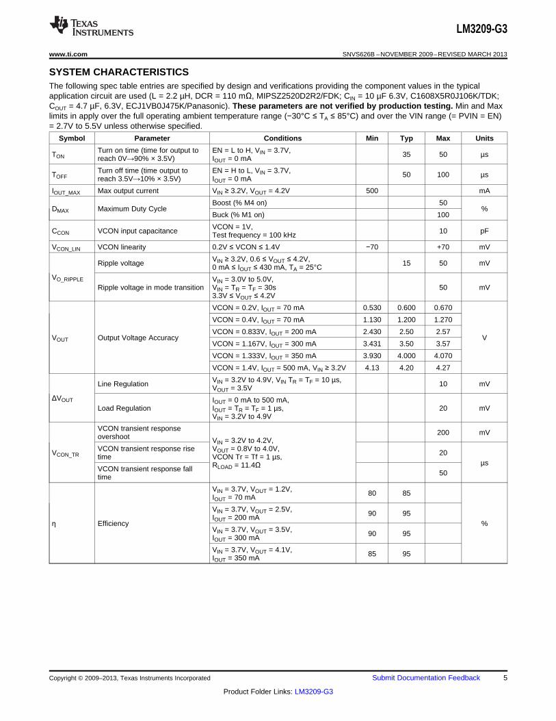
SYSTEM CHARACTERISTICSThe following spec table entries are specified by design and verifications providing the component values in the typicalapplication circuit are used (L = 2.2 µH, DCR = 110 mΩ, MIPSZ2520D2R2/FDK; CIN = 10 µF 6.3V, C1608X5R0J106K/TDK;COUT = 4.7 µF, 6.3V, ECJ1VB0J475K/Panasonic). These parameters are not verified by production testing. Min and Maxlimits in apply over the full operating ambient temperature range (−30°C ≤ TA ≤ 85°C) and over the VIN range (= PVIN = EN)= 2.7V to 5.5V unless otherwise specified.
Symbol Parameter Conditions Min Typ Max Units
Turn on time (time for output to EN = L to H, VIN = 3.7V,TON 35 50 µsreach 0V→90% × 3.5V) IOUT = 0 mA
Turn off time (time output to EN = H to L, VIN = 3.7V,TOFF 50 100 µsreach 3.5V→10% × 3.5V) IOUT = 0 mA
IOUT_MAX Max output current VIN ≥ 3.2V, VOUT = 4.2V 500 mA
SNVS626B –NOVEMBER 2009–REVISED MARCH 2013 www.ti.com
OPERATION DESCRIPTION
The LM3209-G3 buck-boost converter provides high-efficiency, low-noise power for RF power amplifiers (PAs) inmobile phones, portable communicators and similar battery-powered RF devices. It is designed to allow the RFPA to operate at maximum efficiency for a wide range of power levels from a single Li-Ion battery cell. Thecapability of LM3209-G3 to provide an output voltage lower than as well as higher than the input battery voltagealso enables the PA to operate with high linearity for a wide range of battery voltages thereby extending theusable voltage range of the battery. The converter feedback loop is internally compensated for both buck andboost operation and the architecture is such that it provides seamless transition between buck and boost mode ofoperation.
The efficiency of LM3209-G3 is typically around 95% for a 300 mA load with 3.5V output, 3.7V input. TheLM3209-G3 has an RDSON management scheme for low as well as high output voltage. This achieves highefficiency for a wide range of output voltage. The output voltage is dynamically programmable from 0.6V to 4.2Vby adjusting the voltage on the control pin, VCON , without the need for external feedback resistors. The fastoutput voltage transient response of LM3209-G3 makes it suitable for adaptively adjusting the PA supply voltagedepending on its transmitting power which prolongs battery life.
Additional features include current overload protection, output over voltage clamp and thermal overloadshutdown.
The LM3209-G3 is constructed using a chip-scale 12-bump DSBGA package that offers the smallest possiblesize for space-critical applications such as cell phones where board area is an important design consideration.Use of high switching frequency (2.4 MHz, typ.) reduces the size of the external components. As shown inTypical Application Circuit, only three external power components are required for circuit operation. Use of theDSBGA package requires special design considerations for implementation. (See DSBGA PACKAGEASSEMBLY AND USE in the APPLICATION INFORMATION section.) Its fine bump-pitch requires careful boarddesign and precision assembly equipment. Use of this package is best suited for opaque-case applications,where its edges are not subjected to high-intensity ambient red or infrared light.
SHUTDOWN MODE
Setting the EN digital pin low (< 0.6V) places the LM3209-G3 in shutdown mode (0.01 µA ISHDN typ.). Duringshutdown, the output of LM3209-G3 is pulled to ground enabling complete discharge of the output capacitor.Setting EN high (>1.2V) enables normal operation. EN should be set low to turn off the LM3209-G3 duringpower-up and under voltage conditions when the power supply is less than the 2.7V minimum operating voltage.
VCON,ON
The output is disabled when VCON is below 125 mV (typ.). It is enabled when VCON is above 150 mV (typ.).The threshold has approximately 25 mV (typ.) of hysteresis.
RDSON MANAGEMENT
The LM3209-G3 has a unique RDSON management function to improve efficiency in low output voltage as well ashigh output voltage conditions. When VCON < 0.775V (typ.) the device uses only a small part of the PMOS M1to minimize drive loss. When VCON > 0.775V, a large PMOS is also used along with the small PMOS. For RFPAs, the current consumption typically increases with its supply voltage and hence higher supply voltage for thePA also means higher current delivered to it. Adding a large PMOS for VCON > 1.124V reduces the conductionlosses thereby achieving higher efficiency. The LM3209-G3 can also provide output voltages higher than thebattery voltage. This boost mode of operation is typically used when the battery voltage has discharged to a lowvoltage that is not sufficient to provide the required linearity in the PA. A special RDSON management scheme isdesigned for operation well into boost mode such that an auxiliary PMOS switch is also turned on along with thelarge and small PMOS switches. This effectively reduces the RDSON of M1 to a very low value in order to keepthe efficiency maximized. Since M1 conducts all the time in boost mode, reducing the RDSON of M1 achieves asignificant improvement in efficiency.
www.ti.com SNVS626B –NOVEMBER 2009–REVISED MARCH 2013
SUPPLY CURRENT LIMIT
A current limit feature allows the LM3209-G3 to protect itself and external components during overloadconditions. In PWM mode, a 1700 mA (typ.) cycle-by-cycle current limit is normally used when VCON is above0.775V (typ.) and an 850 mA (typ.) limit is used when VCON is below 0.775V (typ.). If an excessive load pulls theoutput voltage down to approximately 0.35V, then the device switches to a timed current limit mode. The currentlimit in this mode is 850 mA (typ.) independent of the set VCON voltage. In timed current limit mode, the internalPMOS M1 is turned off after the current limit is hit and the beginning of the next cycle is inhibited for 3.5 µs toforce the inductor current to ramp down to a safe value.
REVERSE CURRENT LIMIT
Since LM3209-G3 features dynamically adjustable output voltage, the inductor current can build up to highvalues in either direction depending on the output voltage transient. For a low to high output voltage transient,the inductor current flows from SW1 pin to SW2 pin, and this current is limited by the current limit featuremonitoring PMOS M1. For a high to low output voltage transient, the inductor current flows from SW2 pin to SW1pin, and this current needs to be limited to protect the LM3209-G3 as well as the external components. A reversecurrent limit feature allows monitoring the reverse inductor current that also flows through NMOS M2. A -1.2A(typ.) cycle-by-cycle current limit is used to limit the reverse current. When the reverse current hits the reversecurrent limit during a PWM cycle, NMOS M2 is turned off and MOSFET M1 and M4 are turned on for the rest ofthat switching cycle. This allows the inductor to build current in the opposite direction thereby limiting the reversecurrent. It should be noted that the power MOSFET switches M3 and M4 do not have their own current limitingcircuits and are dependent on the current limit operation implemented for power MOSFETs M1 and M2 to protectthem. The implication of this is that any external forcing of voltage/current on SW2 pin or misuse of SW2 pin maybe detrimental to the part and may damage the internal circuits.
DYNAMICALLY ADJUSTABLE OUTPUT VOLTAGE
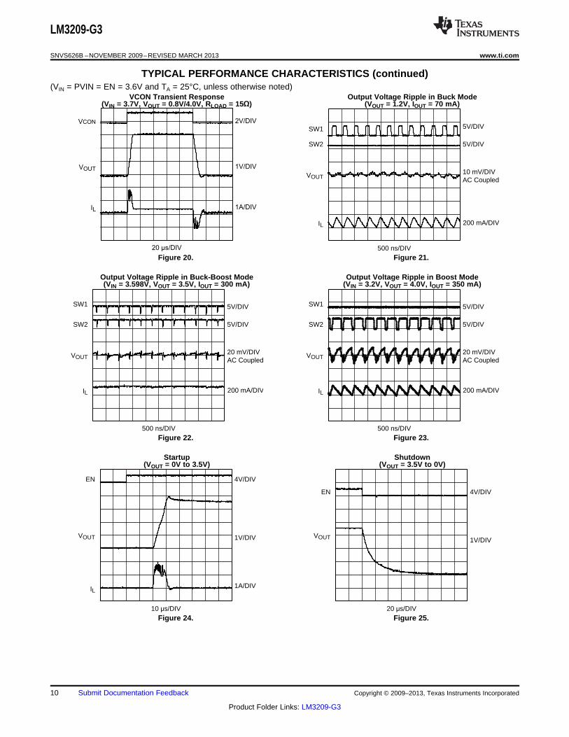
The LM3209-G3 features dynamically adjustable output voltage which eliminates the need for external feedbackresistors. The output can be set from 0.6V to 4.2V by changing the voltage on the analog VCON pin. This featureis useful in cell phone RF PA applications where peak power is needed only when the handset is far away fromthe base station or when data is being transmitted. In other instances, the transmitting power can be reduced.Hence the supply voltage to the PA can be reduced, promoting longer battery life. In order to adaptively adjustthe supply voltage to the PA in real time in a cell phone application, the output voltage transition should be fastenough in order to meet the RF transmit signal specifications. LM3209-G3 offers ultra fast output voltagetransitions without drawing very large currents from the battery supply. With a current limit of 1700 mA (typ.), theoutput voltage can transition from 0.8V to 4.0V in less than 20 µs with a load resistance of 11.4Ω.
SEAMLESS MODE TRANSITION
In a typical non-inverting buck-boost converter, all four power switches, M1 through M4, are switched everycycle. This operation increases MOSFET drive losses and lowers the converter efficiency. The LM3209-G3switches only two power switches every cycle to improve converter efficiency. Hence it operates either as a buckconverter or a boost converter depending upon the input and output voltage conditions. This creates a boundarybetween the buck and boost modes of operation. When the input battery voltage is close to the set outputvoltage, the converter automatically switches to four-switch operation seamlessly such that the output voltagedoes not see any perturbations at the mode boundary. The excellent mode transition capability of LM3209-G3enables low noise output with the highest efficiency. Internal feedback loop compensation ensures stableoperation in buck, boost, as well as the buck-boost mode transition region.
VCON OVER-VOLTAGE CLAMP
The LM3209-G3 features an internal clamp on the analog VCON pin voltage to limit the output voltage to amaximum safe value. The VCON voltage is internally switched to a reference voltage of approximately 1.6Vwhen the VCON in voltage exceeds 1.6V. This limits the output voltage to approximately 4.8V and protects thepart from over voltage stress.
SNVS626B –NOVEMBER 2009–REVISED MARCH 2013 www.ti.com
THERMAL OVERLOAD PROTECTION
The LM3209-G3 has a thermal overload protection function that operates to protect itself from short-term misuseand over-load conditions. When the junction temperature exceeds approximately 150°C, the device inhibitsoperation. All power MOSFET switches are turned off. When the temperature drops below 120°C, normaloperation resumes. Prolonged operation in thermal overload conditions may damage the device and isconsidered bad practice.
www.ti.com SNVS626B –NOVEMBER 2009–REVISED MARCH 2013
APPLICATION INFORMATION
SETTING THE OUTPUT VOLTAGE
The LM3209-G3 features a pin-controlled variable output voltage which eliminates the need for external feedbackresistors. It can be programmed for an output voltage from 0.6V to 4.2V by setting the voltage on the VCON pin,as in the following formula.
VOUT = 3 x VCON (1)
When VCON is between 0.2V and 1.4V, the output voltage will follow this formula.
Internally, VCON is clamped to avoid exceeding the maximum output voltage. When the VCON voltage is greaterthan 1.6V, the output voltage is regulated at approximately 4.8V.
OUTPUT CURRENT CAPABILITY
The LM3209-G3 is designed for a maximum load capability of 650 mA when VIN ≥ 3.0V and 500 mA when VIN <3.0V.
Table 1. Output Voltage vs. Maximum Output Current
VOUT VIN Maximum IOUT
4.2V > 3.0V 650 mA
4.2V ≤ 3.0V 500 mA
3.6V ≥ 3.2V 1000 mA
RECOMMENDED EXTERNAL COMPONENTS
INDUCTOR SELECTION
A 2.2 µH inductor with a saturation current rating over 1900 mA and low inductance drop at the full DC biascondition is recommended for almost all applications. An inductor with a DC resistance of less than 0.1Ω andlower ESR should be used to get good efficiency for the entire output current range.
If an inductance with a lower ISAT rating is used in the application, the VCON Transient Response time will beaffected. The rise time of the output voltage will be increased because the inductor will saturate and cannotcharge the output capacitor quickly enough. If a winding type inductor is selected, the efficiency in light loadconditions may be degraded due to higher ESR losses.
Table 2. Suggested Inductors (2.2 µH)
Vendor Part Number Dimensions (mm) ISAT (30%) IRATING(Δ40°C) DCR (mΩ)
FDK MIPSZ2520D2R2 (2.2 µH) 2.5 x 2.0 x 1.0 1.5A 1.1A 110
Murata LQH2HPN1R0NG0 2.5 x 2.0 x 1.2 1.8A 1.1A 115
Samsung CIG22H2R2MNE 2.5 x 2.0 x 1.2 1.9A 1.6A 116
INPUT CAPACITOR SELECTION
A ceramic input capacitor of 10 µF, 6.3V or higher is sufficient for most applications. Place the input capacitor asclose as possible to the PVIN and PGND pins of the device. A larger value or higher voltage rating may be usedto improve input filtering. Use X7R, X5R, or B types; do not use Y5V or F. DC bias characteristics of ceramiccapacitors must be considered when selecting case sizes like 0603(1608), 0805(2012), or smaller profile. Theinput filter capacitor supplies current to the PMOS switch in the first half of each cycle and reduces the voltageripple imposed on the input power source. A ceramic capacitor's low ESR provides the best noise filtering ofinput voltage spikes caused by this rapidly changing current.
SNVS626B –NOVEMBER 2009–REVISED MARCH 2013 www.ti.com
OUTPUT CAPACITOR SELECTION
Use a 4.7 µF, 6.3V, X7R, X5R, or B types; do not use Y5V or F. DC bias characteristics of ceramic capacitorsmust be considered. DC bias characteristics vary from manufacturer to manufacturer, and DC bias curves shouldbe requested from them as part of the capacitor selection process.
The output filter capacitor smooths out current flow from the inductor to the load, helps maintain a steady outputvoltage during transient load changes and reduces output voltage ripple. These capacitors must be selected withsufficiency capacitance and low ESR to perform these functions. Note that the output voltage ripple is dependenton the inductor current ripple and the Equivalent Series Resistance of the output capacitor (ESR). The ESR isfrequency dependent (as well as temperature dependent); make sure the value used for calculations is at theswitching frequency of the part.
Table 3. SUGGESTED CAPACITORS
Model Vendor
10 µF for CIN
C1608X5R0J106K TDK
4.7 µF for COUT
ECJ1VB0J475K Panasonic
GRM188R60J475ME84D Murata
GRM219R61A475KE19 Murata
RECOMMENDED EXTERNAL COMPONENT COMBINATIONS FOR VCON TRANSIENT
Achieving optimum Output Voltage (VCON) Transient is expected to require both an inductor with smallerinductance degradation and an output capacitor with modest capacitance. FDK MIPSZ2520D2R2 and PanasonicECJ1VB0J475K are one sample of the external component combination.
An inductor with a large inductance drop at high DC bias causes slower charging current to the output capacitor.An output capacitor with less capacitance drop at high voltage will cause a big overshoot. However, an outputcapacitor with a large capacitance drop generates bigger output voltage ripple.
DSBGA PACKAGE ASSEMBLY AND USE
Use of the DSBGA package requires specialized board layout, precision mounting and careful re-flowtechniques, as detailed in Texas Instruments Application Note 1112. Refer to the section Surface MountTechnology (SMD) Assembly Considerations. For best results in assembly, alignment ordinals on the PC boardshould be used to facilitate placement of the device. The pad style used with DSBGA package must be theNSMD (non-solder mask defined) type. This means that the solder-mask opening is larger than the pad size.This prevents a lip that otherwise forms if the solder-mask and pad overlap, from holding the device off thesurface of the board and interfering with mounting. See Application Note 1112 for specific instructions how to dothis.
The 12-bump package used for LM3209-G3 has 300 micron solder balls and requires 10.82 mil pads formounting on the circuit board. The trace to each pad should enter the pad with a 90° entry angle to preventdebris from being caught in deep corners. Initially, the trace to each pad should be 7 mil wide, for a sectionapproximately 7 mil long, as a thermal relief. Then each trance should neck up or down to its optimal width. Theimportant criterion is symmetry. This ensures the solder bumps on the LM3209-G3 re-flow evenly and that thedevice solders level to the board. In particular, special attention must be paid to the pads for bumps A3, B3, andD3. Because PVIN and PGND are typically connected to large copper planes, inadequate thermal relief canresult in late or inadequate re-flow of these bumps.
The DSBGA package is optimized for the smallest possible size in applications with red or infrared opaquecases. Because the DSBGA package lacks the plastic encapsulation characteristic of larger devices, it isvulnerable to light. Backside metallization and/or epoxy coating, along with front-side shading by the printedcircuit board, reduce this sensitivity. However, the package has exposed die edges. In particular, DSBGAdevices are sensitive to light (in the red and infrared range) shining on the package's exposed die edges.
www.ti.com SNVS626B –NOVEMBER 2009–REVISED MARCH 2013
BOARD LAYOUT CONSIDERATIONS
PC board layout is an important part of DC-DC converter design. Poor board layout can disrupt the performanceof a DC-DC converter and surrounding circuitry by contributing to EMI, ground bounce, and resistive voltage lossin the traces.1. Place the LM3209-G3, inductor and filter capacitors close together and make the traces short. The traces
between these components carry relatively high switching currents and act as antennas. Following this rulereduces radiated noise. Special care must be given to place the input filter capacitor very close to the PVINand PGND pins.
2. Connect the ground pins of the LM3209-G3 and filter capacitors together using a generous component-sidecopper fill as a pseudo-ground plane. Then connect this to the ground-plane (if one is used) with severalvias. This reduces ground-plane noise by preventing the switching currents from circulating through theground plane. It also reduces ground bounce at the LM3209-G3 by giving it a low-impedance groundconnection.
3. Use wide traces between the power components and for power connections to the DC-DC converter circuit.This reduces voltage errors caused by resistive losses across the traces.
4. Route noise sensitive traces such as the voltage feedback path away from noisy traces between the powercomponents. The voltage feedback trace must remain close to the LM3209-G3 circuit and should be routeddirectly from FB to VOUT at the output capacitor and should be routed opposite to noisy components. Thisreduces EMI radiated onto the DC-DC converter's own voltage feedback trace.
5. Place noise sensitive circuitry, such as radio IF blocks, away from the DC-DC converter, CMOS digitalblocks, and other noisy circuitry. Interference with noise-sensitive circuitry in the system can be reducedthrough distance.
In mobile phones, for example, a common practice is to place the DC-DC converter on one corner of the board,arrange the CMOS digital circuitry around it (since this also generates noise), and then place sensitivepreamplifiers and IF stages on the diagonally opposing corner. Often, the sensitive circuitry is shielded with ametal pan and power to it is post-regulated to reduce conducted noise, using low-dropout linear regulators.
LM3209TLE-G3/NOPB ACTIVE DSBGA YZR 12 250 Green (RoHS& no Sb/Br)
SNAGCU Level-1-260C-UNLIM -30 to 85 09G3
LM3209TLX-G3/NOPB ACTIVE DSBGA YZR 12 3000 Green (RoHS& no Sb/Br)
SNAGCU Level-1-260C-UNLIM -30 to 85 09G3
(1) The marketing status values are defined as follows:ACTIVE: Product device recommended for new designs.LIFEBUY: TI has announced that the device will be discontinued, and a lifetime-buy period is in effect.NRND: Not recommended for new designs. Device is in production to support existing customers, but TI does not recommend using this part in a new design.PREVIEW: Device has been announced but is not in production. Samples may or may not be available.OBSOLETE: TI has discontinued the production of the device.
(2) Eco Plan - The planned eco-friendly classification: Pb-Free (RoHS), Pb-Free (RoHS Exempt), or Green (RoHS & no Sb/Br) - please check http://www.ti.com/productcontent for the latest availabilityinformation and additional product content details.TBD: The Pb-Free/Green conversion plan has not been defined.Pb-Free (RoHS): TI's terms "Lead-Free" or "Pb-Free" mean semiconductor products that are compatible with the current RoHS requirements for all 6 substances, including the requirement thatlead not exceed 0.1% by weight in homogeneous materials. Where designed to be soldered at high temperatures, TI Pb-Free products are suitable for use in specified lead-free processes.Pb-Free (RoHS Exempt): This component has a RoHS exemption for either 1) lead-based flip-chip solder bumps used between the die and package, or 2) lead-based die adhesive used betweenthe die and leadframe. The component is otherwise considered Pb-Free (RoHS compatible) as defined above.Green (RoHS & no Sb/Br): TI defines "Green" to mean Pb-Free (RoHS compatible), and free of Bromine (Br) and Antimony (Sb) based flame retardants (Br or Sb do not exceed 0.1% by weightin homogeneous material)
(3) MSL, Peak Temp. -- The Moisture Sensitivity Level rating according to the JEDEC industry standard classifications, and peak solder temperature.
(4) There may be additional marking, which relates to the logo, the lot trace code information, or the environmental category on the device.
(5) Multiple Device Markings will be inside parentheses. Only one Device Marking contained in parentheses and separated by a "~" will appear on a device. If a line is indented then it is a continuationof the previous line and the two combined represent the entire Device Marking for that device.
Important Information and Disclaimer:The information provided on this page represents TI's knowledge and belief as of the date that it is provided. TI bases its knowledge and belief on informationprovided by third parties, and makes no representation or warranty as to the accuracy of such information. Efforts are underway to better integrate information from third parties. TI has taken andcontinues to take reasonable steps to provide representative and accurate information but may not have conducted destructive testing or chemical analysis on incoming materials and chemicals.TI and TI suppliers consider certain information to be proprietary, and thus CAS numbers and other limited information may not be available for release.
In no event shall TI's liability arising out of such information exceed the total purchase price of the TI part(s) at issue in this document sold by TI to Customer on an annual basis.
A. All linear dimensions are in millimeters. Dimensioning and tolerancing per ASME Y14.5M-1994.B. This drawing is subject to change without notice.
4215049/A 12/12
NOTES:
D: Max =
E: Max =
2.529 mm, Min =
2.022 mm, Min =
2.469 mm
1.961 mm
IMPORTANT NOTICE
Texas Instruments Incorporated (TI) reserves the right to make corrections, enhancements, improvements and other changes to itssemiconductor products and services per JESD46, latest issue, and to discontinue any product or service per JESD48, latest issue. Buyersshould obtain the latest relevant information before placing orders and should verify that such information is current and complete.TI’s published terms of sale for semiconductor products (http://www.ti.com/sc/docs/stdterms.htm) apply to the sale of packaged integratedcircuit products that TI has qualified and released to market. Additional terms may apply to the use or sale of other types of TI products andservices.Reproduction of significant portions of TI information in TI data sheets is permissible only if reproduction is without alteration and isaccompanied by all associated warranties, conditions, limitations, and notices. TI is not responsible or liable for such reproduceddocumentation. Information of third parties may be subject to additional restrictions. Resale of TI products or services with statementsdifferent from or beyond the parameters stated by TI for that product or service voids all express and any implied warranties for theassociated TI product or service and is an unfair and deceptive business practice. TI is not responsible or liable for any such statements.Buyers and others who are developing systems that incorporate TI products (collectively, “Designers”) understand and agree that Designersremain responsible for using their independent analysis, evaluation and judgment in designing their applications and that Designers havefull and exclusive responsibility to assure the safety of Designers' applications and compliance of their applications (and of all TI productsused in or for Designers’ applications) with all applicable regulations, laws and other applicable requirements. Designer represents that, withrespect to their applications, Designer has all the necessary expertise to create and implement safeguards that (1) anticipate dangerousconsequences of failures, (2) monitor failures and their consequences, and (3) lessen the likelihood of failures that might cause harm andtake appropriate actions. Designer agrees that prior to using or distributing any applications that include TI products, Designer willthoroughly test such applications and the functionality of such TI products as used in such applications.TI’s provision of technical, application or other design advice, quality characterization, reliability data or other services or information,including, but not limited to, reference designs and materials relating to evaluation modules, (collectively, “TI Resources”) are intended toassist designers who are developing applications that incorporate TI products; by downloading, accessing or using TI Resources in anyway, Designer (individually or, if Designer is acting on behalf of a company, Designer’s company) agrees to use any particular TI Resourcesolely for this purpose and subject to the terms of this Notice.TI’s provision of TI Resources does not expand or otherwise alter TI’s applicable published warranties or warranty disclaimers for TIproducts, and no additional obligations or liabilities arise from TI providing such TI Resources. TI reserves the right to make corrections,enhancements, improvements and other changes to its TI Resources. TI has not conducted any testing other than that specificallydescribed in the published documentation for a particular TI Resource.Designer is authorized to use, copy and modify any individual TI Resource only in connection with the development of applications thatinclude the TI product(s) identified in such TI Resource. NO OTHER LICENSE, EXPRESS OR IMPLIED, BY ESTOPPEL OR OTHERWISETO ANY OTHER TI INTELLECTUAL PROPERTY RIGHT, AND NO LICENSE TO ANY TECHNOLOGY OR INTELLECTUAL PROPERTYRIGHT OF TI OR ANY THIRD PARTY IS GRANTED HEREIN, including but not limited to any patent right, copyright, mask work right, orother intellectual property right relating to any combination, machine, or process in which TI products or services are used. Informationregarding or referencing third-party products or services does not constitute a license to use such products or services, or a warranty orendorsement thereof. Use of TI Resources may require a license from a third party under the patents or other intellectual property of thethird party, or a license from TI under the patents or other intellectual property of TI.TI RESOURCES ARE PROVIDED “AS IS” AND WITH ALL FAULTS. TI DISCLAIMS ALL OTHER WARRANTIES ORREPRESENTATIONS, EXPRESS OR IMPLIED, REGARDING RESOURCES OR USE THEREOF, INCLUDING BUT NOT LIMITED TOACCURACY OR COMPLETENESS, TITLE, ANY EPIDEMIC FAILURE WARRANTY AND ANY IMPLIED WARRANTIES OFMERCHANTABILITY, FITNESS FOR A PARTICULAR PURPOSE, AND NON-INFRINGEMENT OF ANY THIRD PARTY INTELLECTUALPROPERTY RIGHTS. TI SHALL NOT BE LIABLE FOR AND SHALL NOT DEFEND OR INDEMNIFY DESIGNER AGAINST ANY CLAIM,INCLUDING BUT NOT LIMITED TO ANY INFRINGEMENT CLAIM THAT RELATES TO OR IS BASED ON ANY COMBINATION OFPRODUCTS EVEN IF DESCRIBED IN TI RESOURCES OR OTHERWISE. IN NO EVENT SHALL TI BE LIABLE FOR ANY ACTUAL,DIRECT, SPECIAL, COLLATERAL, INDIRECT, PUNITIVE, INCIDENTAL, CONSEQUENTIAL OR EXEMPLARY DAMAGES INCONNECTION WITH OR ARISING OUT OF TI RESOURCES OR USE THEREOF, AND REGARDLESS OF WHETHER TI HAS BEENADVISED OF THE POSSIBILITY OF SUCH DAMAGES.Unless TI has explicitly designated an individual product as meeting the requirements of a particular industry standard (e.g., ISO/TS 16949and ISO 26262), TI is not responsible for any failure to meet such industry standard requirements.Where TI specifically promotes products as facilitating functional safety or as compliant with industry functional safety standards, suchproducts are intended to help enable customers to design and create their own applications that meet applicable functional safety standardsand requirements. Using products in an application does not by itself establish any safety features in the application. Designers mustensure compliance with safety-related requirements and standards applicable to their applications. Designer may not use any TI products inlife-critical medical equipment unless authorized officers of the parties have executed a special contract specifically governing such use.Life-critical medical equipment is medical equipment where failure of such equipment would cause serious bodily injury or death (e.g., lifesupport, pacemakers, defibrillators, heart pumps, neurostimulators, and implantables). Such equipment includes, without limitation, allmedical devices identified by the U.S. Food and Drug Administration as Class III devices and equivalent classifications outside the U.S.TI may expressly designate certain products as completing a particular qualification (e.g., Q100, Military Grade, or Enhanced Product).Designers agree that it has the necessary expertise to select the product with the appropriate qualification designation for their applicationsand that proper product selection is at Designers’ own risk. Designers are solely responsible for compliance with all legal and regulatoryrequirements in connection with such selection.Designer will fully indemnify TI and its representatives against any damages, costs, losses, and/or liabilities arising out of Designer’s non-compliance with the terms and provisions of this Notice.