www.ti.com SNVS762B –JANUARY 2000–REVISED MARCH 2013
LM3916 Dot/Bar Display DriverCheck for Samples: LM3916
1FEATURES DESCRIPTIONThe LM3916 is a monolithic integrated circuit that
2• Fast Responding Electronic VU Metersenses analog voltage levels and drives ten LEDs,
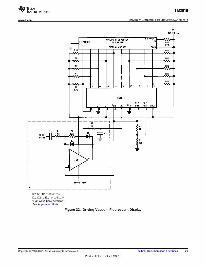
• Drivers LEDs, LCDs, or Vacuum Fluorescents LCDs or vacuum fluorescent displays, providing an• Bar or Dot Display Mode Externally Selectable electronic version of the popular VU meter. One pin
by User changes the display from a bar graph to a moving dotdisplay. LED current drive is regulated and• Expandable to Displays of 70 dBprogrammable, eliminating the need for current
• Internal Voltage Reference from 1.2V to 12V limiting resistors. The whole display system can• Operates with Single Supply of 3V to 25V operate from a single supply as low as 3V or as high
as 25V.• Inputs Operate Down to Ground• Output Current Programmable from 1 mA to 30 The IC contains an adjustable voltage reference and
an accurate ten-step voltage divider. The high-mAimpedance input buffer accepts signals down to• Input Withstands ±35V without Damage orground and up to within 1.5V of the positive supply.False OutputsFurther, it needs no protection against inputs of ±35V.
• Outputs are Current Regulated, Open The input buffer drives 10 individual comparatorsCollectors referenced to the precision divider. Accuracy is
typically better than 0.2 dB.• Directly Drives TTL or CMOS• The Internal 10-step Divider is Floating and Audio applications include average or peak level
indicators, and power meters. Replacing conventionalcan be Referenced to a Wide Range ofmeters with an LED bar graph results in a fasterVoltagesresponding, more rugged display with high visibilityThe LM3916 is Rated for Operation from 0°C tothat retains the ease of interpretation of an analog+70°C. The LM3916N-1 is Available in an 18-display.lead PDIP Package.The LM3916 is extremely easy to apply. A 1.2V full-scale meter requires only one resistor in addition tothe ten LEDs. One more resistor programs the full-scale anywhere from 1.2V to 12V independent ofsupply voltage. LED brightness is easily controlledwith a single pot.
The LM3916 is very versatile. The outputs can driveLCDs, vacuum fluorescents and incandescent bulbsas well as LEDs of any color. Multiple devices can becascaded for a dot or bar mode display for increasedrange and/or resolution. Useful in other applicationsare the linear LM3914 and the logarithmic LM3915.
1
Please be aware that an important notice concerning availability, standard warranty, and use in critical applications ofTexas Instruments semiconductor products and disclaimers thereto appears at the end of this data sheet.
2All trademarks are the property of their respective owners.
SNVS762B –JANUARY 2000–REVISED MARCH 2013 www.ti.com
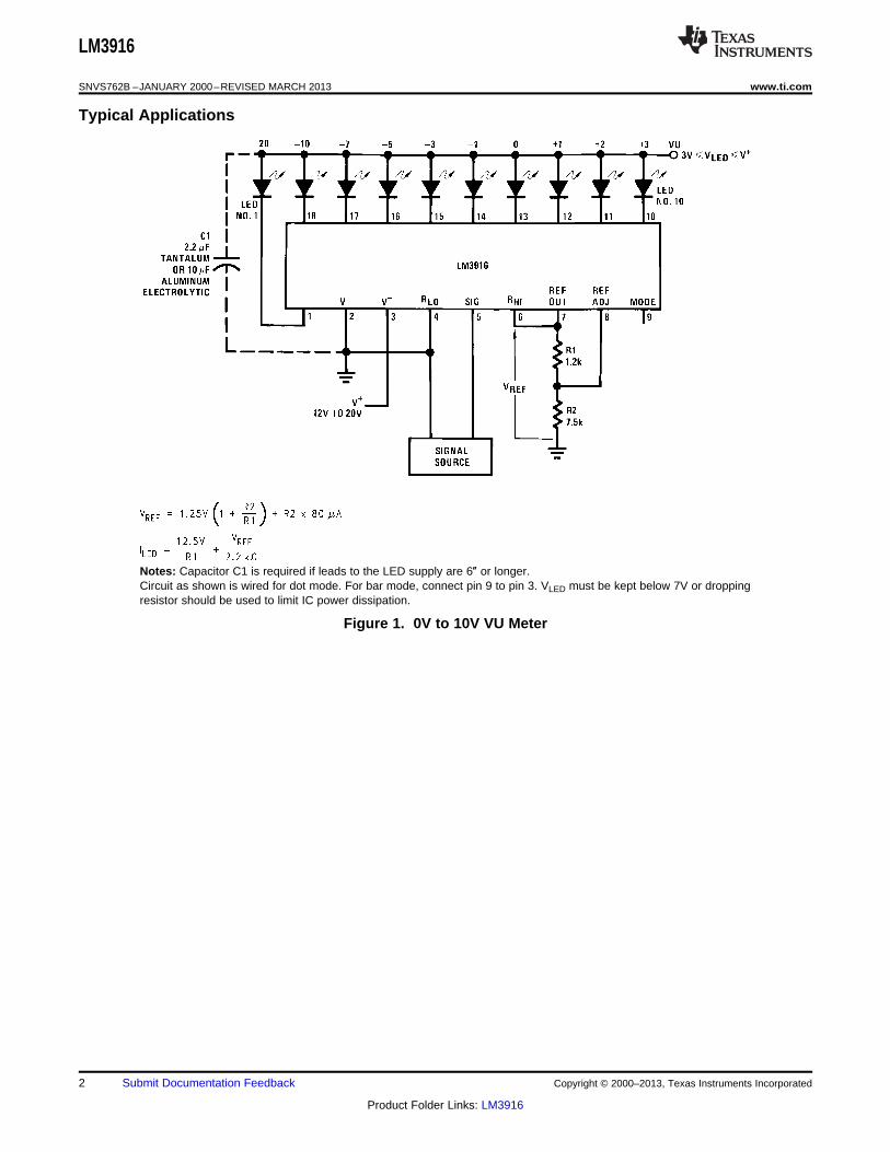
Typical Applications
Notes: Capacitor C1 is required if leads to the LED supply are 6″ or longer.Circuit as shown is wired for dot mode. For bar mode, connect pin 9 to pin 3. VLED must be kept below 7V or droppingresistor should be used to limit IC power dissipation.
www.ti.com SNVS762B –JANUARY 2000–REVISED MARCH 2013
These devices have limited built-in ESD protection. The leads should be shorted together or the device placed in conductive foamduring storage or handling to prevent electrostatic damage to the MOS gates.
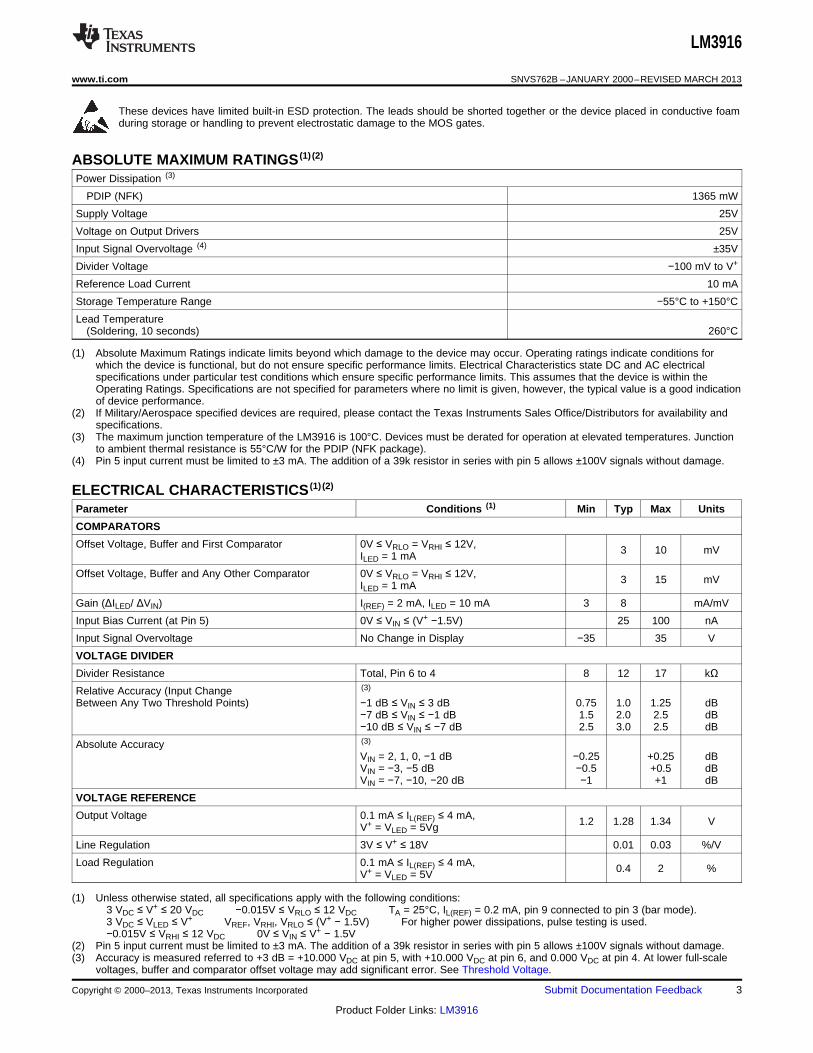
ABSOLUTE MAXIMUM RATINGS (1) (2)
Power Dissipation (3)
PDIP (NFK) 1365 mW
Supply Voltage 25V
Voltage on Output Drivers 25V
Input Signal Overvoltage (4) ±35V
Divider Voltage −100 mV to V+
Reference Load Current 10 mA
Storage Temperature Range −55°C to +150°C
Lead Temperature(Soldering, 10 seconds) 260°C
(1) Absolute Maximum Ratings indicate limits beyond which damage to the device may occur. Operating ratings indicate conditions forwhich the device is functional, but do not ensure specific performance limits. Electrical Characteristics state DC and AC electricalspecifications under particular test conditions which ensure specific performance limits. This assumes that the device is within theOperating Ratings. Specifications are not specified for parameters where no limit is given, however, the typical value is a good indicationof device performance.
(2) If Military/Aerospace specified devices are required, please contact the Texas Instruments Sales Office/Distributors for availability andspecifications.
(3) The maximum junction temperature of the LM3916 is 100°C. Devices must be derated for operation at elevated temperatures. Junctionto ambient thermal resistance is 55°C/W for the PDIP (NFK package).
(4) Pin 5 input current must be limited to ±3 mA. The addition of a 39k resistor in series with pin 5 allows ±100V signals without damage.
ELECTRICAL CHARACTERISTICS (1) (2)
Parameter Conditions (1) Min Typ Max Units
COMPARATORS
Offset Voltage, Buffer and First Comparator 0V ≤ VRLO = VRHI ≤ 12V, 3 10 mVILED = 1 mA
Offset Voltage, Buffer and Any Other Comparator 0V ≤ VRLO = VRHI ≤ 12V, 3 15 mVILED = 1 mA
Gain (ΔILED/ ΔVIN) I(REF) = 2 mA, ILED = 10 mA 3 8 mA/mV
Input Bias Current (at Pin 5) 0V ≤ VIN ≤ (V+ −1.5V) 25 100 nA
Input Signal Overvoltage No Change in Display −35 35 V
(1) Unless otherwise stated, all specifications apply with the following conditions:3 VDC ≤ V+ ≤ 20 VDC −0.015V ≤ VRLO ≤ 12 VDC TA = 25°C, IL(REF) = 0.2 mA, pin 9 connected to pin 3 (bar mode).3 VDC ≤ VLED ≤ V+ VREF, VRHI, VRLO ≤ (V+ − 1.5V) For higher power dissipations, pulse testing is used.−0.015V ≤ VRHI ≤ 12 VDC 0V ≤ VIN ≤ V+ − 1.5V
(2) Pin 5 input current must be limited to ±3 mA. The addition of a 39k resistor in series with pin 5 allows ±100V signals without damage.(3) Accuracy is measured referred to +3 dB = +10.000 VDC at pin 5, with +10.000 VDC at pin 6, and 0.000 VDC at pin 4. At lower full-scale
voltages, buffer and comparator offset voltage may add significant error. See Threshold Voltage.
SNVS762B –JANUARY 2000–REVISED MARCH 2013 www.ti.com
ELECTRICAL CHARACTERISTICS(1)(2) (continued)Parameter Conditions (1) Min Typ Max Units
Output Voltage Change with Temperature 0°C ≤ TA ≤ +70°C, IL(REF) = 1 mA, 1 %V+ = VLED = 5V
Adjust Pin Current 75 120 μA
OUTPUT DRIVERS
LED Current V+ = VLED = 5V, IL(REF) = 1 mA 7 10 13 mA
LED Current Difference (Between Largest and Smallest VLED = 5V, ILED = 2 mA 0.12 0.4 mALED Currents) VLED = 5V, ILED = 20 mA 1.2 3 mA
LED Current Regulation 2V ≤ VLED ≤ 17VILED 2 mA 0.1 0.25 mAILED = 20 mA 1 3 mA
Dropout Voltage ILED(ON) = 20 mA @ VLED = 5V, 1.5 VΔILED = 2 mA
Saturation Voltage ILED = 2.0 mA, IL(REF) = 0.4 mA 0.15 0.4 V
Output Leakage, Each Collector Bar Mode (4) 0.1 100 μA
Output Leakage Dot Mode (4)
Pins 10–18 0.1 100 μA
Pin 1 60 150 450 μA
SUPPLY CURRENT
Standby Supply Current V+ = + 5V, IL(REF) = 0.2 mA 2.4 4.2 mA(All Outputs Off) V+ = + 20V, IL(REF) = 1.0 mA 6.1 9.2 mA
(4) Bar mode results when pin 9 is within 20 mV of V+. Dot mode results when pin 9 is pulled at least 200 mV below V+. LED #10 (pin 10output current) is disabled if pin 9 is pulled 0.9V or more below VLED.
(1) Accuracy is measured referred to +3 dB = +10.000 VDC at pin 5, with +10.000 VDC at pin 6, and 0.000 VDC at pin 4. At lower full-scalevoltages, buffer and comparator offset voltage may add significant error. See Threshold Voltage.
SNVS762B –JANUARY 2000–REVISED MARCH 2013 www.ti.com
FUNCTIONAL DESCRIPTION
The simplified LM3916 block diagram is included to give the general idea of the circuit's operation. A high inputimpedance buffer operates with signals from ground to 12V, and is protected against reverse and overvoltagesignals. The signal is then applied to a series of 10 comparators; each of which is biased to a differentcomparison level by the resistor string.
In the example illustrated, the resistor string is connected to the internal 1.25V reference voltage. As the inputvoltage varies from 0 to 1.25, the comparator outputs are driven low one by one, switching on the LED indicators.The resistor divider can be connected between any 2 voltages, providing that they are at least 1.5V below V+ andno lower than V−.
INTERNAL VOLTAGE REFERENCE
The reference is designed to be adjustable and develops a nominal 1.25V between the REF OUT (pin 7) andREF ADJ (pin 8) terminals. The reference voltage is impressed across program resistor R1 and, since thevoltage is constant, a constant current I1 then flows through the output set resistor R2 giving an output voltage of:
Since the 120 μA current (max) from the adjust terminal represents an error term, the reference was designed tominimize changes of this current with V+ and load changes. For correct operation, reference load current shouldbe between 80 μA and 5 mA. Load capacitance should be less than 0.05 μF.
CURRENT PROGRAMMING
A feature not completely illustrated by the block diagram is the LED brightness control. The current drawn out ofthe reference voltage pin (pin 7) determines LED current. Approximately 10 times this current will be drawnthrough each lighted LED, and this current will be relatively constant despite supply voltage and temperaturechanges. Current drawn by the internal 10-resistor divider, as well as by the external current and voltage-settingdivider should be included in calculating LED drive current. The ability to modulate LED brightness with time, orin proportion to input voltage and other signals can lead to a number of novel displays or ways of indicating inputovervoltages, alarms, etc.
The LM3916 outputs are current-limited NPN transistors as shown below. An internal feedback loop regulatesthe transistor drive. Output current is held at about 10 times the reference load current, independent of outputvoltage and processing variables, as long as the transistor is not saturated.
www.ti.com SNVS762B –JANUARY 2000–REVISED MARCH 2013
Figure 14. LM3916 Output Circuit
Outputs may be run in saturation with no adverse effects, making it possible to directly drive logic. The effectivesaturation resistance of the output transistors, equal to RE plus the transistors' collector resistance, is about 50Ω.It's also possible to drive LEDs from rectified AC with no filtering. To avoid oscillations, the LED supply should bebypassed with a 2.2 μF tantalum or 10 μF aluminum electrolytic capacitor.
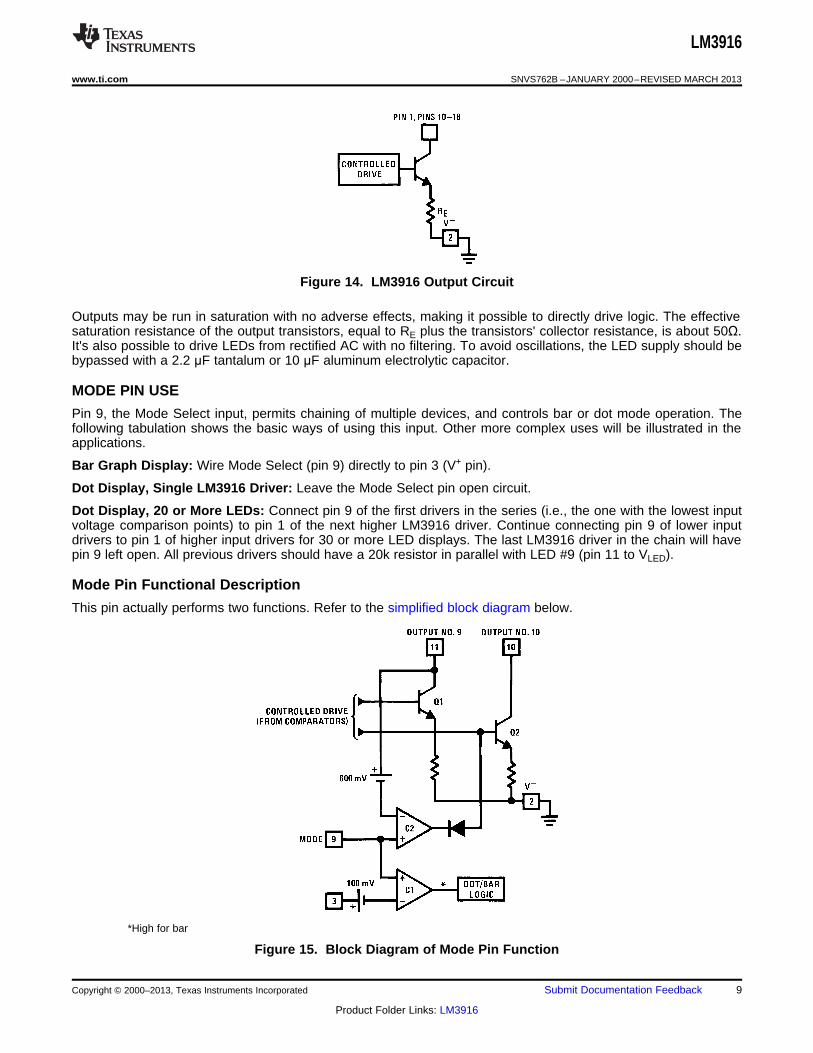
MODE PIN USE
Pin 9, the Mode Select input, permits chaining of multiple devices, and controls bar or dot mode operation. Thefollowing tabulation shows the basic ways of using this input. Other more complex uses will be illustrated in theapplications.
Bar Graph Display: Wire Mode Select (pin 9) directly to pin 3 (V+ pin).
Dot Display, Single LM3916 Driver: Leave the Mode Select pin open circuit.
Dot Display, 20 or More LEDs: Connect pin 9 of the first drivers in the series (i.e., the one with the lowest inputvoltage comparison points) to pin 1 of the next higher LM3916 driver. Continue connecting pin 9 of lower inputdrivers to pin 1 of higher input drivers for 30 or more LED displays. The last LM3916 driver in the chain will havepin 9 left open. All previous drivers should have a 20k resistor in parallel with LED #9 (pin 11 to VLED).
Mode Pin Functional Description
This pin actually performs two functions. Refer to the simplified block diagram below.
SNVS762B –JANUARY 2000–REVISED MARCH 2013 www.ti.com
DOT OR BAR MODE SELECTION
The voltage at pin 9 is sensed by comparator C1, nominally referenced to (V+ −100 mV). The chip is in bar modewhen pin 9 is above this level; otherwise it's in dot mode. The comparator is designed so that pin 9 can be leftopen circuit for dot mode.
Taking into account comparator gain and variation in the 100 mV reference level, pin 9 should be no more than20 mV below V+ for bar mode and more than 200 mV below V+ (or open circuit) for dot mode. In mostapplications, pin 9 is either open (dot mode) or tied to V+ (bar mode). In bar mode, pin 9 should be connecteddirectly to pin 3. Large currents drawn from the power supply (LED current, for example) should not share thispath so that large IR drops are avoided.
DOT MODE CARRY
In order for display to make sense when multiple drivers are cascaded in dot mode, special circuitry has beenincluded to shut off LED #10 of the first device when LED #1 of the second device comes on. The connection forcascading in dot mode has already been described and is depicted in Figure 16.
As long as the input signal voltage is below the threshold of the second driver, LED #11 is off. Pin 9 of driver #1thus sees effectively an open circuit so the chip is in dot mode. As soon as the input voltage reaches thethreshold of LED #11, pin 9 of driver #1 is pulled an LED drop (1.5V or more) below VLED. This condition issensed by comparator C2, referenced 600 mV below VLED. This forces the output of C2 low, which shuts offoutput transistor Q2, extinguishing LED #10.
VLED is sensed via the 20k resistor connected to pin 11. The very small current (less than 100 μA) that is divertedfrom LED #9 does not noticeably affect its intensity.
An auxiliary current source at pin 1 keeps at least 100 μA flowing through LED #11 even if the input voltage riseshigh enough to extinguish the LED. This ensures that pin 9 of driver #1 is held low enough to force LED #10 offwhen any higher LED is illuminated. While 100 μA does not normally produce significant LED illumination, it maybe noticeable when using high-efficiency LEDs in a dark environment. If this is bothersome, the simple cure is toshunt LED #11 (and LED #1) with a 10k resistor. The 1V 1R drop is more than the 900 mV worst case requiredto hold off LED #10 yet small enough that LED #11 does not conduct significantly.
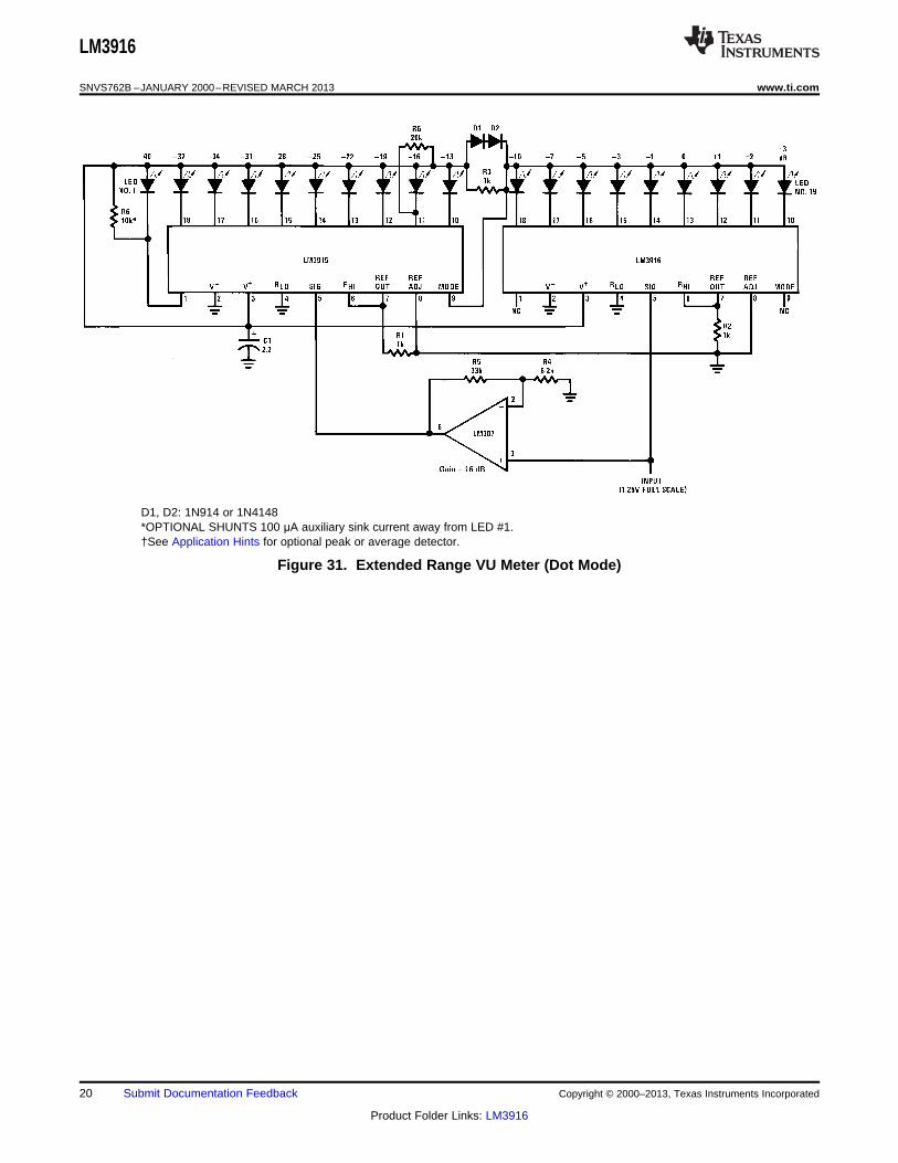
In some circuits a number of outputs on the higher device are not used. Examples include the high resolution VUmeter and the expanded range VU meter circuits (see Typical Applications). To provide the proper carry sensevoltage in dot mode, the LEDs of the higher driver IC are tied to VLED through two series-connected diodes asshown in Figure 17. Shunting the diodes with a 1k resistor provides a path for driver leakage current.
Figure 16. Cascading LM3914/15/16 Series in Dot Mode
www.ti.com SNVS762B –JANUARY 2000–REVISED MARCH 2013
Figure 17. Cascading Drivers in Dot Mode with Pin 1 of Driver #2 Unused
OTHER DEVICE CHARACTERISTICS
The LM3915 is relatively low-powered itself, and since any number of LEDs can be powered from about 3V, it isa very efficient display driver. Typical standby supply current (all LEDs OFF) is 1.6 mA. However, any referenceloading adds 4 times that current drain to the V+ (pin 3) supply input. For example, an LM3915 with a 1 mAreference pin load (1.3k) would supply almost 10 mA to every LED while drawing only 10 mA from its V+ pinsupply. At full-scale, the IC is typically drawing less than 10% of the current supplied to the display.
The display driver does not have built-in hysteresis so that the display does not jump instantly from one LED tothe next. Under rapidly changing signal conditions, this cuts down high frequency noise and often an annoyingflicker. An “overlap” is built in so that at no time are all segments completely off the dot mode. Generally one LEDfades in while the other fades out over a 1 mV range. The change may be much more rapid between LED #10 ofone device and LED #1 of a second device cascaded.
Application Hints
The most difficult problem occurs when large LED currents are being drawn, especially in bar graph mode.These currents flowing out of the ground pin cause voltage drops in external wiring, and thus errors andoscillations. Bringing the return wires from signal sources, reference ground and bottom of the resistor string to asingle point very near pin 2 is the best solution.
Long wires from VLED to LED anode common can cause oscillations. The usual cure is bypassing the LEDanodes with a 2.2 μF tantalum or 10 μF aluminum electrolytic capacitor. If the LED anode line wiring isinaccessible, often a 0.1 μF capacitor from pin 1 to pin 2 will be sufficient.
If there is a large amount of LED overlap in the bar mode, oscillation or excessive noise is usually the problem.In cases where proper wiring and bypassing fail to stop oscillations, V+ voltage at pin 3 is usually belowsuggested limits. When several LEDs are lit in dot mode, the problem is usually an AC component of the inputsignal which should be filtered out. Expanded scale meter applications may have one or both ends of the internalvoltage divider terminated at relatively high value resistors. These high-impedance ends should be bypassed topin 2 with 0.1 μF.
Power dissipation, especially in bar mode should be given consideration. For example, with a 5V supply and allLEDs programmed to 20 mA the driver will dissipate over 600 mW. In this case a 7.5Ω resistor in series with theLED supply will cut device heating in half. The negative end of the resistor should be bypassed with a 2.2 μFsolid tantalum or 10 μF aluminum electrolytic capacitor to pin 2.
TIPS ON RECTIFIER CIRCUITS
The simplest way to display an AC signal using the LM3916 is to apply it right to pin 5 unrectified. Since the LEDilluminated represents the instantaneous value of the AC waveform, one can readily discern both peak andaverage values of audio signals in this manner. The LM3916 will respond to positive half-cycles only but will notbe damaged by signals up to ±35V (or up to ±100V if a 39k resistor is in series with the input). A smear or bartype display results even though the LM3916 is connected for dot mode. The LEDs should be run at 20 mA to 30mA for high enough average intensity.
SNVS762B –JANUARY 2000–REVISED MARCH 2013 www.ti.com
True average or peak detection requires rectification. If an LM3916 is set up with 10V full scale across its voltagedivider, the turn-on point for the first LED is only 450 mV. A simple silicon diode rectifier won't work well at thelow end due to the 600 mV diode threshold. The half-wave peak detector in Figure 18 uses a PNP emitter-follower in front of the diode. Now, the transistor's base-emitter voltage cancels out the diode offset, within about100 mV. This approach is usually satisfactory when a single LM3916 is used for a 23 dB display.
Display circuits such as the extended range VU meter using two or more drivers for a dynamic range of 40 dB orgreater require more accurate detection. In the precision half-wave rectifier of Figure 19 the effective diode offsetis reduced by a factor equal to the open-loop gain of the op amp. Filter capacitor C2 charges through R3 anddischarges through R2 and R3, so that appropriate selection of these values results in either a peak or anaverage detector. The circuit has a gain equal to R2/R1.
It's best to capacitively couple the input. Audio sources frequently have a small DC offset that can causesignificant error at the low end of the log display. Op amps that slew quickly, such as the LF351, LF353 orLF356, are needed to faithfully respond to sudden transients. It may be necessary to trim out the op amp DCoffset voltage to accurately cover a 60 dB range. Best results are obtained if the circuit is adjusted for the correctoutput when a low-level AC signal (10 to 20 mV) is applied, rather than adjusting for zero output with zero input.
*DC Couple
Figure 18. Half-Wave Peak Detector
D1, D2: 1N914 or 1N4148
Average Peak
R2 1k 100k
R3 100k 1k
R1 = R2 for AV = 1R1 = R2/10 for AV = 10C1 = 10/R1
www.ti.com SNVS762B –JANUARY 2000–REVISED MARCH 2013
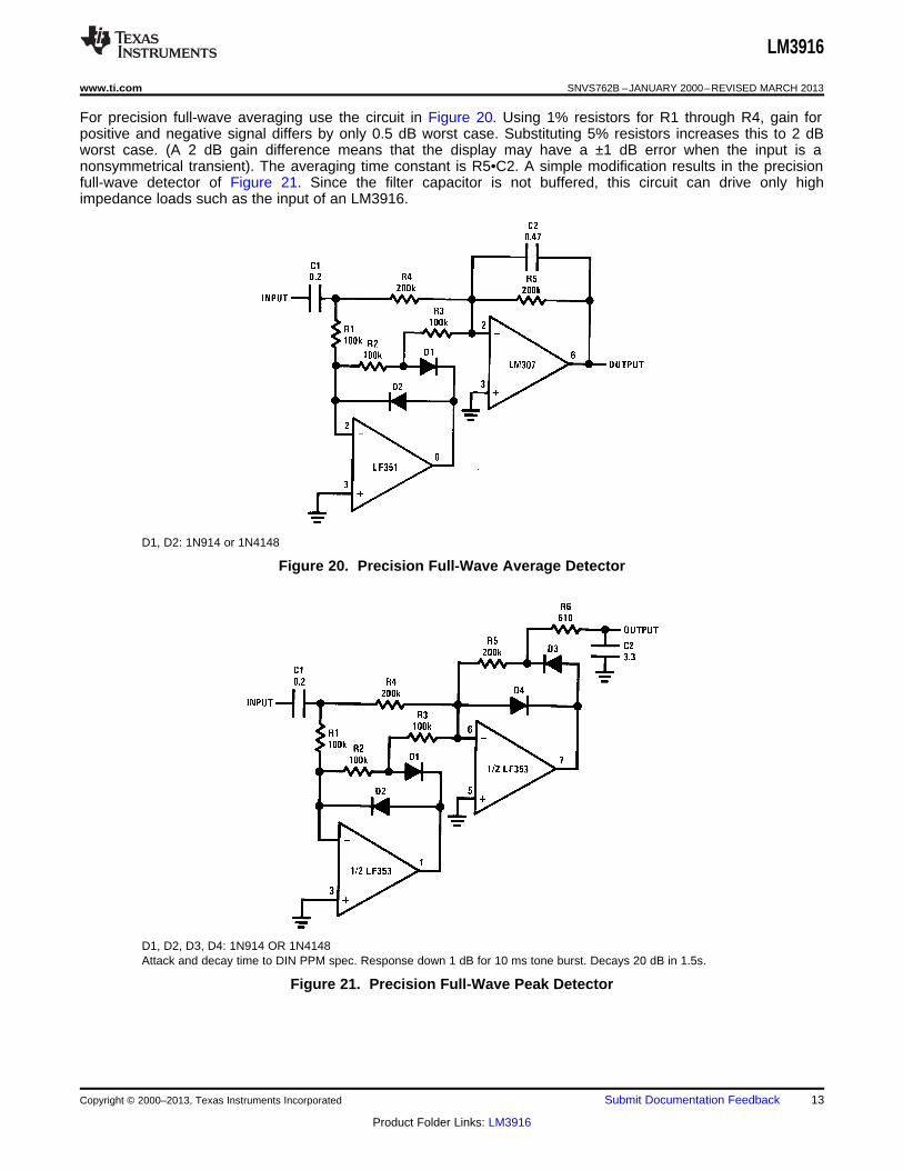
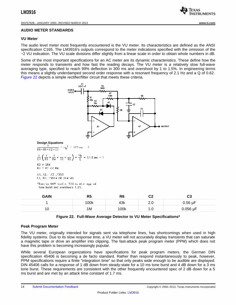
For precision full-wave averaging use the circuit in Figure 20. Using 1% resistors for R1 through R4, gain forpositive and negative signal differs by only 0.5 dB worst case. Substituting 5% resistors increases this to 2 dBworst case. (A 2 dB gain difference means that the display may have a ±1 dB error when the input is anonsymmetrical transient). The averaging time constant is R5•C2. A simple modification results in the precisionfull-wave detector of Figure 21. Since the filter capacitor is not buffered, this circuit can drive only highimpedance loads such as the input of an LM3916.
D1, D2: 1N914 or 1N4148
Figure 20. Precision Full-Wave Average Detector
D1, D2, D3, D4: 1N914 OR 1N4148Attack and decay time to DIN PPM spec. Response down 1 dB for 10 ms tone burst. Decays 20 dB in 1.5s.
SNVS762B –JANUARY 2000–REVISED MARCH 2013 www.ti.com
AUDIO METER STANDARDS
VU Meter
The audio level meter most frequently encountered is the VU meter. Its characteristics are defined as the ANSIspecification C165. The LM3916's outputs correspond to the meter indications specified with the omission of the−2 VU indication. The VU scale divisions differ slightly from a linear scale in order to obtain whole numbers in dB.
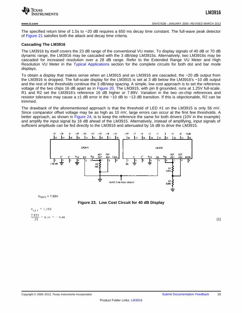
Some of the most important specifications for an AC meter are its dynamic characteristics. These define how themeter responds to transients and how fast the reading decays. The VU meter is a relatively slow full-waveaveraging type, specified to reach 99% deflection in 300 ms and overshoot by 1 to 1.5%. In engineering termsthis means a slightly underdamped second order response with a resonant frequency of 2.1 Hz and a Q of 0.62.Figure 22 depicts a simple rectifier/filter circuit that meets these criteria.
Design Equations
GAIN R5 R6 C2 C3
1 100k 43k 2.0 0.56 μF
10 1M 100k 1.0 0.056 μF
Figure 22. Full-Wave Average Detector to VU Meter Specifications*
Peak Program Meter
The VU meter, originally intended for signals sent via telephone lines, has shortcomings when used in highfidelity systems. Due to its slow response time, a VU meter will not accurately display transients that can saturatea magnetic tape or drive an amplifier into clipping. The fast-attack peak program meter (PPM) which does nothave this problem is becoming increasingly popular.
While several European organizations have specifications for peak program meters, the German DINspecification 45406 is becoming a de facto standard. Rather than respond instantaneously to peak, however,PPM specifications require a finite “integration time” so that only peaks wide enough to be audible are displayed.DIN 45406 calls for a response of 1 dB down from steady-state for a 10 ms tone burst and 4 dB down for a 3 mstone burst. These requirements are consistent with the other frequently encountered spec of 2 dB down for a 5ms burst and are met by an attack time constant of 1.7 ms.
www.ti.com SNVS762B –JANUARY 2000–REVISED MARCH 2013
The specified return time of 1.5s to −20 dB requires a 650 ms decay time constant. The full-wave peak detectorof Figure 21 satisfies both the attack and decay time criteria.
Cascading The LM3916
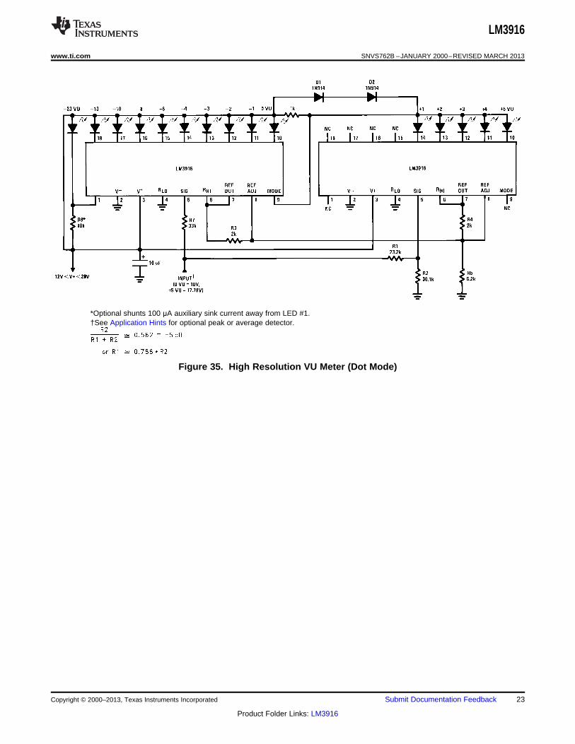
The LM3916 by itself covers the 23 dB range of the conventional VU meter. To display signals of 40 dB or 70 dBdynamic range, the LM3916 may be cascaded with the 3 dB/step LM3915s. Alternatively, two LM3916s may becascaded for increased resolution over a 28 dB range. Refer to the Extended Range VU Meter and HighResolution VU Meter in the Typical Applications section for the complete circuits for both dot and bar modedisplays.
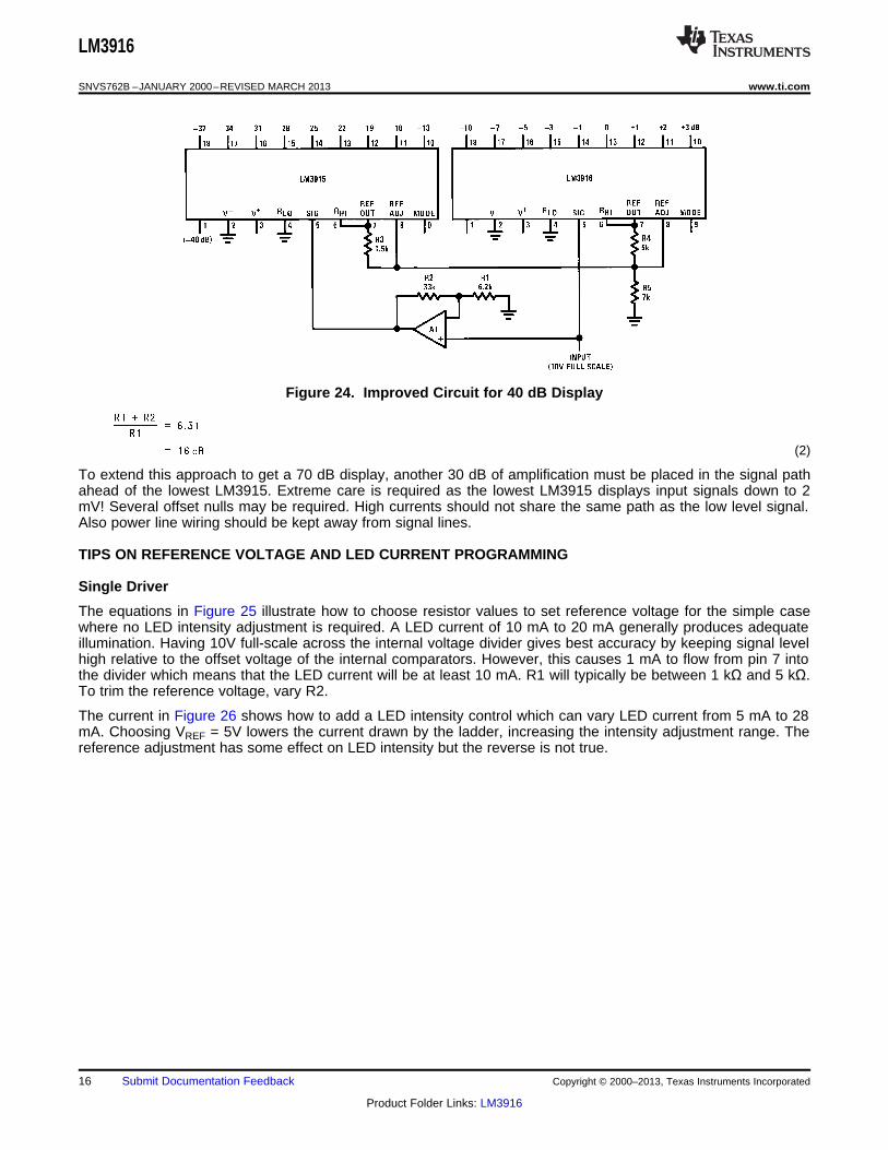
To obtain a display that makes sense when an LM3915 and an LM3916 are cascaded, the −20 dB output fromthe LM3916 is dropped. The full-scale display for the LM3915 is set at 3 dB below the LM3916's −10 dB outputand the rest of the thresholds continue the 3 dB/step spacing. A simple, low cost approach is to set the referencevoltage of the two chips 16 dB apart as in Figure 20. The LM3915, with pin 8 grounded, runs at 1.25V full-scale.R1 and R2 set the LM3916's reference 16 dB higher or 7.89V. Variation in the two on-chip references andresistor tolerance may cause a ±1 dB error in the −10 dB to −13 dB transition. If this is objectionable, R2 can betrimmed.
The drawback of the aforementioned approach is that the threshold of LED #1 on the LM3915 is only 56 mV.Since comparator offset voltage may be as high as 10 mV, large errors can occur at the first few thresholds. Abetter approach, as shown in Figure 24, is to keep the reference the same for both drivers (10V in the example)and amplify the input signal by 16 dB ahead of the LM3915. Alternatively, instead of amplifying, input signals ofsufficient amplitude can be fed directly to the LM3916 and attenuated by 16 dB to drive the LM3915.
SNVS762B –JANUARY 2000–REVISED MARCH 2013 www.ti.com
Figure 24. Improved Circuit for 40 dB Display
(2)
To extend this approach to get a 70 dB display, another 30 dB of amplification must be placed in the signal pathahead of the lowest LM3915. Extreme care is required as the lowest LM3915 displays input signals down to 2mV! Several offset nulls may be required. High currents should not share the same path as the low level signal.Also power line wiring should be kept away from signal lines.
TIPS ON REFERENCE VOLTAGE AND LED CURRENT PROGRAMMING
Single Driver
The equations in Figure 25 illustrate how to choose resistor values to set reference voltage for the simple casewhere no LED intensity adjustment is required. A LED current of 10 mA to 20 mA generally produces adequateillumination. Having 10V full-scale across the internal voltage divider gives best accuracy by keeping signal levelhigh relative to the offset voltage of the internal comparators. However, this causes 1 mA to flow from pin 7 intothe divider which means that the LED current will be at least 10 mA. R1 will typically be between 1 kΩ and 5 kΩ.To trim the reference voltage, vary R2.
The current in Figure 26 shows how to add a LED intensity control which can vary LED current from 5 mA to 28mA. Choosing VREF = 5V lowers the current drawn by the ladder, increasing the intensity adjustment range. Thereference adjustment has some effect on LED intensity but the reverse is not true.
www.ti.com SNVS762B –JANUARY 2000–REVISED MARCH 2013
Figure 25. Design Equations for Fixed LED Intensity
5 mA ≤ ILED ≤ 28 mA @ VREF = 5V
Figure 26. Varying LED Intensity
Multiple Drivers
Figure 27 shows how to obtain a common reference trim and intensity control for two drivers. The two ICs maybe connected in cascade or may be handling separate channels for stereo. This technique can be extended forlarger numbers of drivers by varying the values of R1, R2 and R3. Because the LM3915 has a greater ladderresistance, R5 was picked less than R7 in such a way as to provide equal reference load currents. The ICs'internal references track within 100 mV so that worst case error from chip to chip is only 0.2 dB for VREF = 5V.
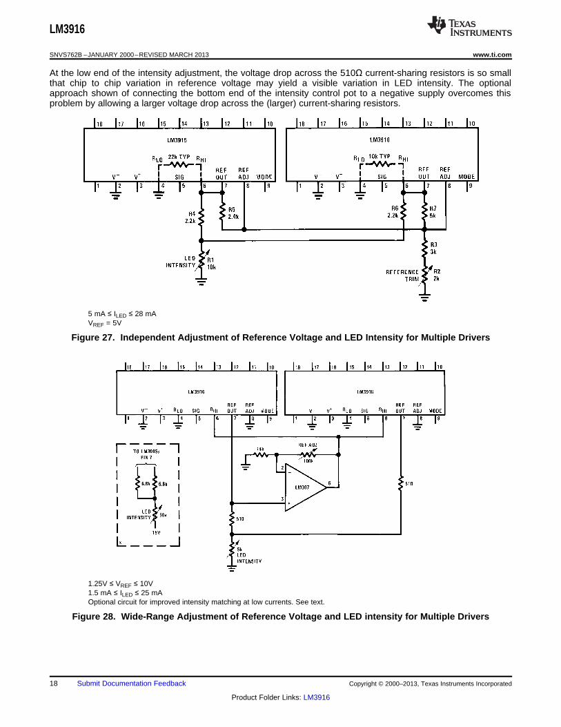
The scheme in Figure 28 is useful when the reference and LED intensity must be adjusted independently over awide range. The RHI voltage can be adjusted from 1.2V to 10V with no effect on LED current. Since the internaldivider here does not load down the reference, minimum LED current is much lower. At the minimumrecommended reference load of 80 μA, LED current is about 0.8 mA. The resistor values shown give a LEDcurrent range from 1.5 mA to 25 mA.
SNVS762B –JANUARY 2000–REVISED MARCH 2013 www.ti.com
At the low end of the intensity adjustment, the voltage drop across the 510Ω current-sharing resistors is so smallthat chip to chip variation in reference voltage may yield a visible variation in LED intensity. The optionalapproach shown of connecting the bottom end of the intensity control pot to a negative supply overcomes thisproblem by allowing a larger voltage drop across the (larger) current-sharing resistors.
5 mA ≤ ILED ≤ 28 mAVREF = 5V
Figure 27. Independent Adjustment of Reference Voltage and LED Intensity for Multiple Drivers
1.25V ≤ VREF ≤ 10V1.5 mA ≤ ILED ≤ 25 mAOptional circuit for improved intensity matching at low currents. See text.
Figure 28. Wide-Range Adjustment of Reference Voltage and LED intensity for Multiple Drivers
www.ti.com SNVS762B –JANUARY 2000–REVISED MARCH 2013
Other Applications
For increased resolution, it's possible to obtain a display with a smooth transition between LEDs. This isaccomplished by superimposing an AC waveform on top of the input level as shown in Figure 29. The signal canbe a triangle, sawtooth or sine wave from 60 Hz to 1 kHz. The display can be run in either dot or bar mode.
Figure 29. 0V to 10V VU Meter with Smooth Transitions
Typical Applications
This application shows that the LED supply requires minimal filtering.*See Application Hints for optional Peak or Average Detector.†Adjust R3 for 3 dB difference between LED #11 and LED #12
SNVS762B –JANUARY 2000–REVISED MARCH 2013 www.ti.com
*The input to the Dot-Bar switch may be taken from cathodes of other LEDs. Display will change to bar as soon asthe LED so selected begins to light.**Optional. Shunts 100 μA auxiliary sink current away from LED #1.
Figure 33. Indicator and Alarm, Full-Scale Changes Display From Dot to Bar
*See Application Hints for optional peak or average detector.
www.ti.com SNVS762B –JANUARY 2000–REVISED MARCH 2013
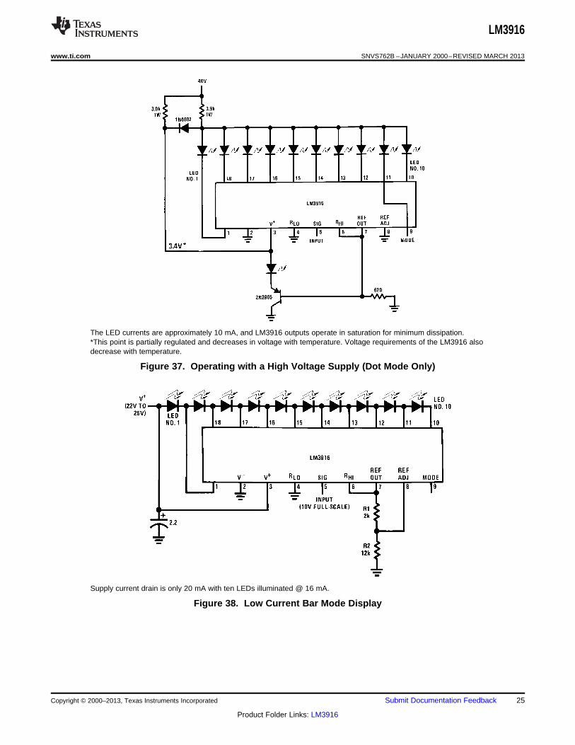
The LED currents are approximately 10 mA, and LM3916 outputs operate in saturation for minimum dissipation.*This point is partially regulated and decreases in voltage with temperature. Voltage requirements of the LM3916 alsodecrease with temperature.
Figure 37. Operating with a High Voltage Supply (Dot Mode Only)
Supply current drain is only 20 mA with ten LEDs illuminated @ 16 mA.
SNVS762B –JANUARY 2000–REVISED MARCH 2013 www.ti.com
Figure 39. Driving Liquid Crystal Display
Full-scale causes the full bar display to flash. If the junction of R1 and C1 is connected to a different LED cathode, thedisplay will flash when that LED lights, and at any higher input signal.
www.ti.com SNVS762B –JANUARY 2000–REVISED MARCH 2013
Connection Diagram
Figure 41. Top ViewPDIP Package
See Package Number NFK0018A
Definition of Terms
Absolute Accuracy: The difference between the observed threshold voltage and the ideal threshold voltage foreach comparator. Specified and tested with 10V across the internal voltage divider so that resistor ratiomatching error predominates over comparator offset voltage.
Adjust Pin Current: Current flowing out of the reference amplifier pin when the reference amplifier is in thelinear region.
Comparator Gain: The ratio of the change in output current (ILED) to the change in input voltage (VIN) requiredto produce it for a comparator in the linear region.
Dropout Voltage: The voltage measured at the current source outputs required to make the output current fallby 10%.
Input Bias Current: Current flowing out of the signal input when the input buffer is in the linear region.
LED Current Regulation: The change in output current over the specified range of LED supply voltage (VLED)as measured at the current source outputs. As the forward voltage of an LED does not changesignificantly with a small change in forward current, this is equivalent to changing the voltage at the LEDanodes by the same amount.
Line Regulation: The average change in reference output voltage (VREF) over the specified range of supplyvoltage (V+).
Load Regulation: The change in reference output voltage over the specified range of load current (IL(REF)).
Offset Voltage: The differential input voltage which must be applied to each comparator to bias the output inthe linear region. Most significant error when the voltage across the internal voltage divider is small.Specified and tested with pin 6 voltage (VRHI) equal to pin 4 voltage (VRLO).
Relative Accuracy: The difference between any two adjacent threshold points. Specified and tested with 10Vacross the internal voltage divider so that resistor ratio matching error predominates over comparatoroffset voltage.
SNVS762B –JANUARY 2000–REVISED MARCH 2013 www.ti.com
REVISION HISTORY
Changes from Revision A (March 2013) to Revision B Page
• Changed layout of National Data Sheet to TI format .......................................................................................................... 27
LM3916N-1 ACTIVE PDIP NFK 18 20 TBD Call TI Call TI 0 to 70 LM3916N-1
LM3916N-1/NOPB ACTIVE PDIP NFK 18 20 Green (RoHS& no Sb/Br)
Call TI Level-1-NA-UNLIM 0 to 70 LM3916N-1
(1) The marketing status values are defined as follows:ACTIVE: Product device recommended for new designs.LIFEBUY: TI has announced that the device will be discontinued, and a lifetime-buy period is in effect.NRND: Not recommended for new designs. Device is in production to support existing customers, but TI does not recommend using this part in a new design.PREVIEW: Device has been announced but is not in production. Samples may or may not be available.OBSOLETE: TI has discontinued the production of the device.
(2) Eco Plan - The planned eco-friendly classification: Pb-Free (RoHS), Pb-Free (RoHS Exempt), or Green (RoHS & no Sb/Br) - please check http://www.ti.com/productcontent for the latest availabilityinformation and additional product content details.TBD: The Pb-Free/Green conversion plan has not been defined.Pb-Free (RoHS): TI's terms "Lead-Free" or "Pb-Free" mean semiconductor products that are compatible with the current RoHS requirements for all 6 substances, including the requirement thatlead not exceed 0.1% by weight in homogeneous materials. Where designed to be soldered at high temperatures, TI Pb-Free products are suitable for use in specified lead-free processes.Pb-Free (RoHS Exempt): This component has a RoHS exemption for either 1) lead-based flip-chip solder bumps used between the die and package, or 2) lead-based die adhesive used betweenthe die and leadframe. The component is otherwise considered Pb-Free (RoHS compatible) as defined above.Green (RoHS & no Sb/Br): TI defines "Green" to mean Pb-Free (RoHS compatible), and free of Bromine (Br) and Antimony (Sb) based flame retardants (Br or Sb do not exceed 0.1% by weightin homogeneous material)
(3) MSL, Peak Temp. -- The Moisture Sensitivity Level rating according to the JEDEC industry standard classifications, and peak solder temperature.
(4) There may be additional marking, which relates to the logo, the lot trace code information, or the environmental category on the device.
(5) Multiple Device Markings will be inside parentheses. Only one Device Marking contained in parentheses and separated by a "~" will appear on a device. If a line is indented then it is a continuationof the previous line and the two combined represent the entire Device Marking for that device.
Important Information and Disclaimer:The information provided on this page represents TI's knowledge and belief as of the date that it is provided. TI bases its knowledge and belief on informationprovided by third parties, and makes no representation or warranty as to the accuracy of such information. Efforts are underway to better integrate information from third parties. TI has taken andcontinues to take reasonable steps to provide representative and accurate information but may not have conducted destructive testing or chemical analysis on incoming materials and chemicals.TI and TI suppliers consider certain information to be proprietary, and thus CAS numbers and other limited information may not be available for release.
In no event shall TI's liability arising out of such information exceed the total purchase price of the TI part(s) at issue in this document sold by TI to Customer on an annual basis.
Texas Instruments Incorporated and its subsidiaries (TI) reserve the right to make corrections, enhancements, improvements and otherchanges to its semiconductor products and services per JESD46, latest issue, and to discontinue any product or service per JESD48, latestissue. Buyers should obtain the latest relevant information before placing orders and should verify that such information is current andcomplete. All semiconductor products (also referred to herein as “components”) are sold subject to TI’s terms and conditions of salesupplied at the time of order acknowledgment.
TI warrants performance of its components to the specifications applicable at the time of sale, in accordance with the warranty in TI’s termsand conditions of sale of semiconductor products. Testing and other quality control techniques are used to the extent TI deems necessaryto support this warranty. Except where mandated by applicable law, testing of all parameters of each component is not necessarilyperformed.
TI assumes no liability for applications assistance or the design of Buyers’ products. Buyers are responsible for their products andapplications using TI components. To minimize the risks associated with Buyers’ products and applications, Buyers should provideadequate design and operating safeguards.
TI does not warrant or represent that any license, either express or implied, is granted under any patent right, copyright, mask work right, orother intellectual property right relating to any combination, machine, or process in which TI components or services are used. Informationpublished by TI regarding third-party products or services does not constitute a license to use such products or services or a warranty orendorsement thereof. Use of such information may require a license from a third party under the patents or other intellectual property of thethird party, or a license from TI under the patents or other intellectual property of TI.
Reproduction of significant portions of TI information in TI data books or data sheets is permissible only if reproduction is without alterationand is accompanied by all associated warranties, conditions, limitations, and notices. TI is not responsible or liable for such altereddocumentation. Information of third parties may be subject to additional restrictions.
Resale of TI components or services with statements different from or beyond the parameters stated by TI for that component or servicevoids all express and any implied warranties for the associated TI component or service and is an unfair and deceptive business practice.TI is not responsible or liable for any such statements.
Buyer acknowledges and agrees that it is solely responsible for compliance with all legal, regulatory and safety-related requirementsconcerning its products, and any use of TI components in its applications, notwithstanding any applications-related information or supportthat may be provided by TI. Buyer represents and agrees that it has all the necessary expertise to create and implement safeguards whichanticipate dangerous consequences of failures, monitor failures and their consequences, lessen the likelihood of failures that might causeharm and take appropriate remedial actions. Buyer will fully indemnify TI and its representatives against any damages arising out of the useof any TI components in safety-critical applications.
In some cases, TI components may be promoted specifically to facilitate safety-related applications. With such components, TI’s goal is tohelp enable customers to design and create their own end-product solutions that meet applicable functional safety standards andrequirements. Nonetheless, such components are subject to these terms.
No TI components are authorized for use in FDA Class III (or similar life-critical medical equipment) unless authorized officers of the partieshave executed a special agreement specifically governing such use.
Only those TI components which TI has specifically designated as military grade or “enhanced plastic” are designed and intended for use inmilitary/aerospace applications or environments. Buyer acknowledges and agrees that any military or aerospace use of TI componentswhich have not been so designated is solely at the Buyer's risk, and that Buyer is solely responsible for compliance with all legal andregulatory requirements in connection with such use.
TI has specifically designated certain components as meeting ISO/TS16949 requirements, mainly for automotive use. In any case of use ofnon-designated products, TI will not be responsible for any failure to meet ISO/TS16949.
Products Applications
Audio www.ti.com/audio Automotive and Transportation www.ti.com/automotive
Amplifiers amplifier.ti.com Communications and Telecom www.ti.com/communications
Data Converters dataconverter.ti.com Computers and Peripherals www.ti.com/computers