LM3916Dot/Bar Display DriverGeneral DescriptionThe LM3916 is a monolithic integrated circuit that sensesanalog voltage levels and drives ten LEDs, LCDs or vacuumfluorescent displays, providing an electronic version of thepopular VU meter. One pin changes the display from a bargraph to a moving dot display. LED current drive is regulatedand programmable, eliminating the need for current limitingresistors. The whole display system can operate from asingle supply as low as 3V or as high as 25V.
The IC contains an adjustable voltage reference and an ac-curate ten-step voltage divider. The high-impedance inputbuffer accepts signals down to ground and up to within 1.5Vof the positive supply. Further, it needs no protection againstinputs of ±35V. The input buffer drives 10 individual com-parators referenced to the precision divider. Accuracy is typi-cally better than 0.2 dB.
Audio applications include average or peak level indicators,and power meters. Replacing conventional meters with anLED bar graph results in a faster responding, more ruggeddisplay with high visibility that retains the ease of interpreta-tion of an analog display.
The LM3916 is extremely easy to apply. A 1.2V full-scalemeter requires only one resistor in addition to the ten LEDs.One more resistor programs the full-scale anywhere from1.2V to 12V independent of supply voltage. LED brightnessis easily controlled with a single pot.
The LM3916 is very versatile. The outputs can drive LCDs,vacuum fluorescents and incandescent bulbs as well asLEDs of any color. Multiple devices can be cascaded for adot or bar mode display for increased range and/or resolu-tion. Useful in other applications are the linear LM3914 andthe logarithmic LM3915.
Featuresn Fast responding electronic VU metern Drivers LEDs, LCDs, or vacuum fluorescentsn Bar or dot display mode externally selectable by usern Expandable to displays of 70 dBn Internal voltage reference from 1.2V to 12Vn Operates with single supply of 3V to 25Vn Inputs operate down to groundn Output current programmable from 1 mA to 30 mAn Input withstands ±35V without damage or false outputsn Outputs are current regulated, open collectorsn Directly drives TTL or CMOSn The internal 10-step divider is floating and can be
referenced to a wide range of voltages
The LM3916 is rated for operation from 0˚C to +70˚C. TheLM3916N-1 is available in an 18-lead molded DIP package.
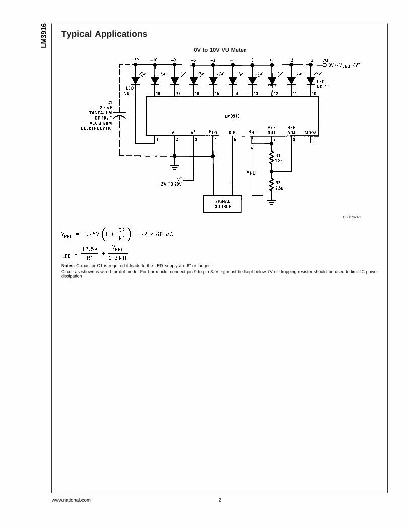
Notes: Capacitor C1 is required if leads to the LED supply are 6" or longer.Circuit as shown is wired for dot mode. For bar mode, connect pin 9 to pin 3. VLED must be kept below 7V or dropping resistor should be used to limit IC powerdissipation.
LM39
16
www.national.com 2
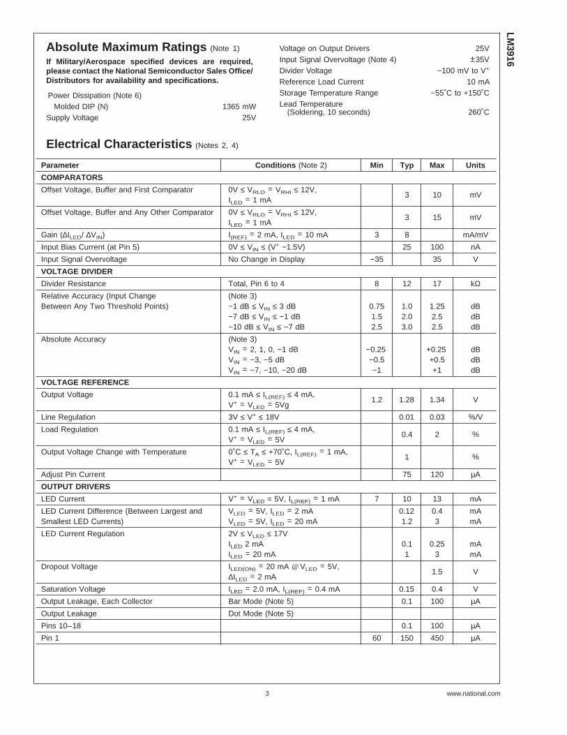
Absolute Maximum Ratings (Note 1)
If Military/Aerospace specified devices are required,please contact the National Semiconductor Sales Office/Distributors for availability and specifications.
Power Dissipation (Note 6)Molded DIP (N) 1365 mW
Supply Voltage 25V
Voltage on Output Drivers 25VInput Signal Overvoltage (Note 4) ±35VDivider Voltage −100 mV to V+
Reference Load Current 10 mAStorage Temperature Range −55˚C to +150˚CLead Temperature
(Soldering, 10 seconds) 260˚C
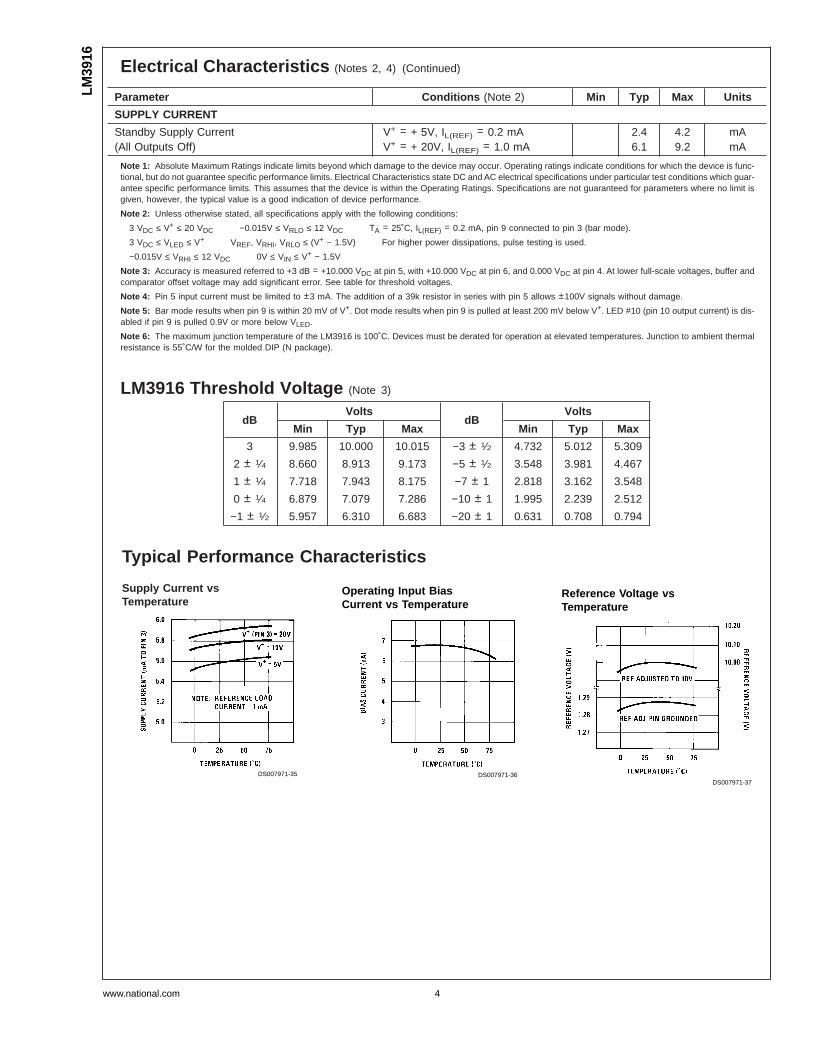
Electrical Characteristics (Notes 2, 4)
Parameter Conditions (Note 2) Min Typ Max Units
COMPARATORS
Offset Voltage, Buffer and First Comparator 0V ≤ VRLO = VRHI ≤ 12V,ILED = 1 mA
3 10 mV
Offset Voltage, Buffer and Any Other Comparator 0V ≤ VRLO = VRHI ≤ 12V,ILED = 1 mA
3 15 mV
Gain (∆ILED/ ∆VIN) I(REF) = 2 mA, ILED = 10 mA 3 8 mA/mV
Input Bias Current (at Pin 5) 0V ≤ VIN ≤ (V+ −1.5V) 25 100 nA
Input Signal Overvoltage No Change in Display −35 35 V
VOLTAGE DIVIDER
Divider Resistance Total, Pin 6 to 4 8 12 17 kΩRelative Accuracy (Input ChangeBetween Any Two Threshold Points)
(Note 3)−1 dB ≤ VIN ≤ 3 dB−7 dB ≤ VIN ≤ −1 dB−10 dB ≤ VIN ≤ −7 dB
Note 1: Absolute Maximum Ratings indicate limits beyond which damage to the device may occur. Operating ratings indicate conditions for which the device is func-tional, but do not guarantee specific performance limits. Electrical Characteristics state DC and AC electrical specifications under particular test conditions which guar-antee specific performance limits. This assumes that the device is within the Operating Ratings. Specifications are not guaranteed for parameters where no limit isgiven, however, the typical value is a good indication of device performance.
Note 2: Unless otherwise stated, all specifications apply with the following conditions:
3 VDC ≤ V+ ≤ 20 VDC −0.015V ≤ VRLO ≤ 12 VDC TA = 25˚C, IL(REF) = 0.2 mA, pin 9 connected to pin 3 (bar mode).
3 VDC ≤ VLED ≤ V+ VREF, VRHI, VRLO ≤ (V+ − 1.5V) For higher power dissipations, pulse testing is used.
−0.015V ≤ VRHI ≤ 12 VDC 0V ≤ VIN ≤ V+ − 1.5V
Note 3: Accuracy is measured referred to +3 dB = +10.000 VDC at pin 5, with +10.000 VDC at pin 6, and 0.000 VDC at pin 4. At lower full-scale voltages, buffer andcomparator offset voltage may add significant error. See table for threshold voltages.
Note 4: Pin 5 input current must be limited to ±3 mA. The addition of a 39k resistor in series with pin 5 allows ±100V signals without damage.
Note 5: Bar mode results when pin 9 is within 20 mV of V+. Dot mode results when pin 9 is pulled at least 200 mV below V+. LED #10 (pin 10 output current) is dis-abled if pin 9 is pulled 0.9V or more below VLED.
Note 6: The maximum junction temperature of the LM3916 is 100˚C. Devices must be derated for operation at elevated temperatures. Junction to ambient thermalresistance is 55˚C/W for the molded DIP (N package).
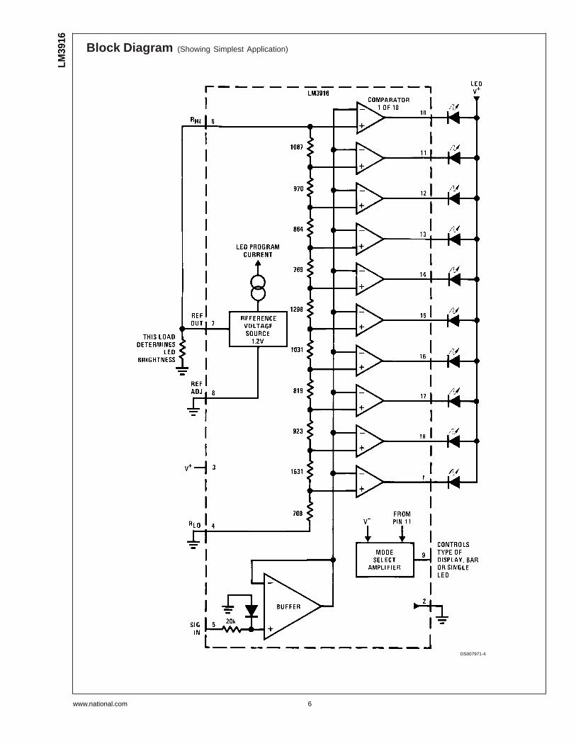
Functional DescriptionThe simplified LM3916 block diagram is included to give thegeneral idea of the circuit’s operation. A high input imped-ance buffer operates with signals from ground to 12V, and isprotected against reverse and overvoltage signals. The sig-nal is then applied to a series of 10 comparators; each ofwhich is biased to a different comparison level by the resistorstring.
In the example illustrated, the resistor string is connected tothe internal 1.25V reference voltage. As the input voltagevaries from 0 to 1.25, the comparator outputs are driven lowone by one, switching on the LED indicators. The resistor di-vider can be connected between any 2 voltages, providingthat they are at least 1.5V below V+ and no lower than V−.
INTERNAL VOLTAGE REFERENCE
The reference is designed to be adjustable and develops anominal 1.25V between the REF OUT (pin 7) and REF ADJ(pin 8) terminals. The reference voltage is impressed acrossprogram resistor R1 and, since the voltage is constant, aconstant current I1 then flows through the output set resistorR2 giving an output voltage of:
Since the 120 µA current (max) from the adjust terminal rep-resents an error term, the reference was designed to mini-mize changes of this current with V+ and load changes. Forcorrect operation, reference load current should be between80 µA and 5 mA. Load capacitance should be less than0.05 µF.
CURRENT PROGRAMMING
A feature not completely illustrated by the block diagram isthe LED brightness control. The current drawn out of the ref-erence voltage pin (pin 7) determines LED current. Approxi-mately 10 times this current will be drawn through eachlighted LED, and this current will be relatively constant de-spite supply voltage and temperature changes. Currentdrawn by the internal 10-resistor divider, as well as by the ex-ternal current and voltage-setting divider should be includedin calculating LED drive current. The ability to modulate LEDbrightness with time, or in proportion to input voltage andother signals can lead to a number of novel displays or waysof indicating input overvoltages, alarms, etc.
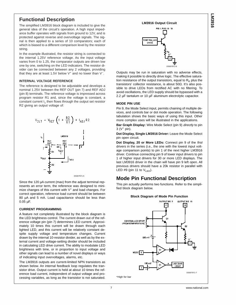
The LM3916 outputs are current-limited NPN transistors asshown below. An internal feedback loop regulates the tran-sistor drive. Output current is held at about 10 times the ref-erence load current, independent of output voltage and pro-cessing variables, as long as the transistor is not saturated.
Outputs may be run in saturation with no adverse effects,making it possible to directly drive logic. The effective satura-tion resistance of the output transistors, equal to RE plus thetransistors’ collector resistance, is about 50Ω. It’s also pos-sible to drive LEDs from rectified AC with no filtering. Toavoid oscillations, the LED supply should be bypassed with a2.2 µF tantalum or 10 µF aluminum electrolytic capacitor.
MODE PIN USE
Pin 9, the Mode Select input, permits chaining of multiple de-vices, and controls bar or dot mode operation. The followingtabulation shows the basic ways of using this input. Othermore complex uses will be illustrated in the applications.
Bar Graph Display: Wire Mode Select (pin 9) directly to pin3 (V+ pin).
Dot Display, Single LM3916 Driver: Leave the Mode Selectpin open circuit.
Dot Display, 20 or More LEDs: Connect pin 9 of the firstdrivers in the series (i.e., the one with the lowest input volt-age comparison points) to pin 1 of the next higher LM3916driver. Continue connecting pin 9 of lower input drivers to pin1 of higher input drivers for 30 or more LED displays. Thelast LM3916 driver in the chain will have pin 9 left open. Allprevious drivers should have a 20k resistor in parallel withLED #9 (pin 11 to VLED).
Mode Pin Functional DescriptionThis pin actually performs two functions. Refer to the simpli-fied block diagram below.
DS007971-5
LM3916 Output Circuit
DS007971-6
Block Diagram of Mode Pin Function
DS007971-7
*High for bar
LM3916
www.national.com7
Mode Pin Functional Description(Continued)
DOT OR BAR MODE SELECTION
The voltage at pin 9 is sensed by comparator C1, nominallyreferenced to (V+ −100 mV). The chip is in bar mode whenpin 9 is above this level; otherwise it’s in dot mode. The com-parator is designed so that pin 9 can be left open circuit fordot mode.
Taking into account comparator gain and variation in the100 mV reference level, pin 9 should be no more than 20 mVbelow V+ for bar mode and more than 200 mV below V+ (oropen circuit) for dot mode. In most applications, pin 9 is ei-ther open (dot mode) or tied to V+ (bar mode). In bar mode,pin 9 should be connected directly to pin 3. Large currentsdrawn from the power supply (LED current, for example)should not share this path so that large IR drops are avoided.
DOT MODE CARRY
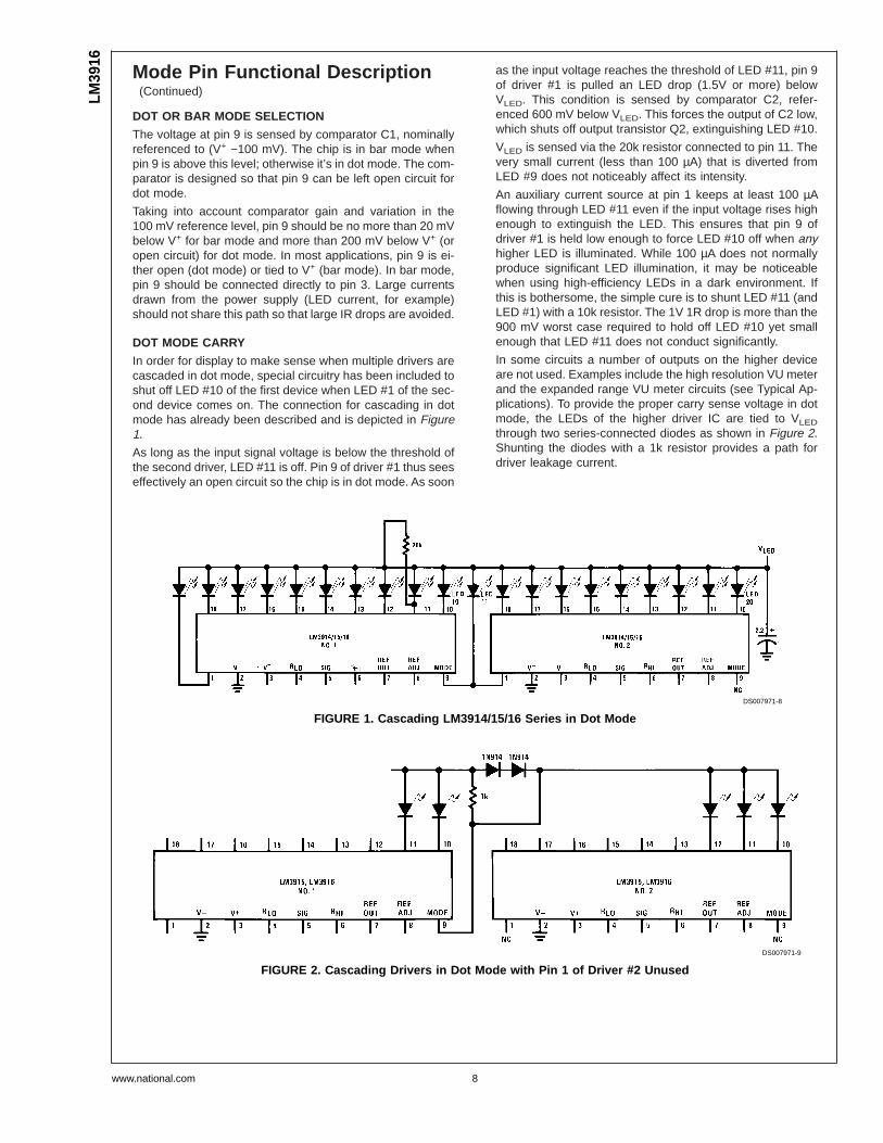
In order for display to make sense when multiple drivers arecascaded in dot mode, special circuitry has been included toshut off LED #10 of the first device when LED #1 of the sec-ond device comes on. The connection for cascading in dotmode has already been described and is depicted in Figure1.
As long as the input signal voltage is below the threshold ofthe second driver, LED #11 is off. Pin 9 of driver #1 thus seeseffectively an open circuit so the chip is in dot mode. As soon
as the input voltage reaches the threshold of LED #11, pin 9of driver #1 is pulled an LED drop (1.5V or more) belowVLED. This condition is sensed by comparator C2, refer-enced 600 mV below VLED. This forces the output of C2 low,which shuts off output transistor Q2, extinguishing LED #10.
VLED is sensed via the 20k resistor connected to pin 11. Thevery small current (less than 100 µA) that is diverted fromLED #9 does not noticeably affect its intensity.
An auxiliary current source at pin 1 keeps at least 100 µAflowing through LED #11 even if the input voltage rises highenough to extinguish the LED. This ensures that pin 9 ofdriver #1 is held low enough to force LED #10 off when anyhigher LED is illuminated. While 100 µA does not normallyproduce significant LED illumination, it may be noticeablewhen using high-efficiency LEDs in a dark environment. Ifthis is bothersome, the simple cure is to shunt LED #11 (andLED #1) with a 10k resistor. The 1V 1R drop is more than the900 mV worst case required to hold off LED #10 yet smallenough that LED #11 does not conduct significantly.
In some circuits a number of outputs on the higher deviceare not used. Examples include the high resolution VU meterand the expanded range VU meter circuits (see Typical Ap-plications). To provide the proper carry sense voltage in dotmode, the LEDs of the higher driver IC are tied to VLED
through two series-connected diodes as shown in Figure 2.Shunting the diodes with a 1k resistor provides a path fordriver leakage current.
DS007971-8
FIGURE 1. Cascading LM3914/15/16 Series in Dot Mode
DS007971-9
FIGURE 2. Cascading Drivers in Dot Mode with Pin 1 of Driver #2 Unused
LM39
16
www.national.com 8
Mode Pin Functional Description(Continued)
OTHER DEVICE CHARACTERISTICS
The LM3915 is relatively low-powered itself, and since anynumber of LEDs can be powered from about 3V, it is a veryefficient display driver. Typical standby supply current (allLEDs OFF) is 1.6 mA. However, any reference loading adds4 times that current drain to the V+ (pin 3) supply input. Forexample, an LM3915 with a 1 mA reference pin load (1.3k)would supply almost 10 mA to every LED while drawing only10 mA from its V+ pin supply. At full-scale, the IC is typicallydrawing less than 10% of the current supplied to the display.
The display driver does not have built-in hysteresis so thatthe display does not jump instantly from one LED to the next.Under rapidly changing signal conditions, this cuts downhigh frequency noise and often an annoying flicker. An “over-lap” is built in so that at no time are all segments completelyoff the dot mode. Generally one LED fades in while the otherfades out over a 1 mV range. The change may be muchmore rapid between LED #10 of one device and LED #1 of asecond device cascaded.
Application HintsThe most difficult problem occurs when large LED currentsare being drawn, especially in bar graph mode. These cur-rents flowing out of the ground pin cause voltage drops in ex-ternal wiring, and thus errors and oscillations. Bringing thereturn wires from signal sources, reference ground and bot-tom of the resistor string to a single point very near pin 2 isthe best solution.
Long wires from VLED to LED anode common can cause os-cillations. The usual cure is bypassing the LED anodes witha 2.2 µF tantalum or 10 µF aluminum electrolytic capacitor. Ifthe LED anode line wiring is inaccessible, often a 0.1 µF ca-pacitor from pin 1 to pin 2 will be sufficient.
If there is a large amount of LED overlap in the bar mode, os-cillation or excessive noise is usually the problem. In caseswhere proper wiring and bypassing fail to stop oscillations,V+ voltage at pin 3 is usually below suggested limits. Whenseveral LEDs are lit in dot mode, the problem is usually anAC component of the input signal which should be filteredout. Expanded scale meter applications may have one orboth ends of the internal voltage divider terminated at rela-tively high value resistors. These high-impedance endsshould be bypassed to pin 2 with 0.1 µF.
Power dissipation, especially in bar mode should be givenconsideration. For example, with a 5V supply and all LEDsprogrammed to 20 mA the driver will dissipate over 600 mW.In this case a 7.5Ω resistor in series with the LED supply willcut device heating in half. The negative end of the resistorshould be bypassed with a 2.2 µF solid tantalum or 10 µFaluminum electrolytic capacitor to pin 2.
TIPS ON RECTIFIER CIRCUITS
The simplest way to display an AC signal using the LM3916is to apply it right to pin 5 unrectified. Since the LED illumi-nated represents the instantaneous value of the AC wave-form, one can readily discern both peak and average valuesof audio signals in this manner. The LM3916 will respond topositive half-cycles only but will not be damaged by signalsup to ±35V (or up to ±100V if a 39k resistor is in series withthe input). A smear or bar type display results even thoughthe LM3916 is connected for dot mode. The LEDs should berun at 20 mA to 30 mA for high enough average intensity.
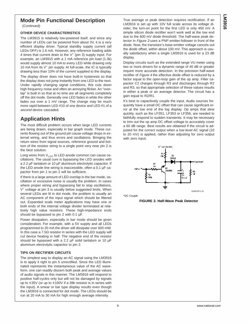
True average or peak detection requires rectification. If anLM3916 is set up with 10V full scale across its voltage di-vider, the turn-on point for the first LED is only 450 mV. Asimple silicon diode rectifier won’t work well at the low enddue to the 600 mV diode threshold. The half-wave peak de-tector in Figure 3 uses a PNP emitter-follower in front of thediode. Now, the transistor’s base-emitter voltage cancels outthe diode offset, within about 100 mV. This approach is usu-ally satisfactory when a single LM3916 is used for a 23 dBdisplay.
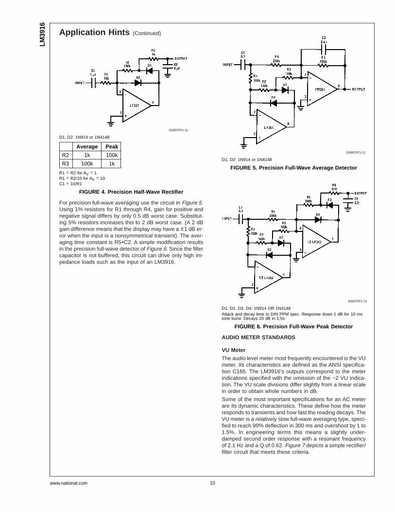
Display circuits such as the extended range VU meter usingtwo or more drivers for a dynamic range of 40 dB or greaterrequire more accurate detection. In the precision half-waverectifier of Figure 4 the effective diode offset is reduced by afactor equal to the open-loop gain of the op amp. Filter ca-pacitor C2 charges through R3 and discharges through R2and R3, so that appropriate selection of these values resultsin either a peak or an average detector. The circuit has again equal to R2/R1.
It’s best to capacitively couple the input. Audio sources fre-quently have a small DC offset that can cause significant er-ror at the low end of the log display. Op amps that slewquickly, such as the LF351, LF353 or LF356, are needed tofaithfully respond to sudden transients. It may be necessaryto trim out the op amp DC offset voltage to accurately covera 60 dB range. Best results are obtained if the circuit is ad-justed for the correct output when a low-level AC signal (10to 20 mV) is applied, rather than adjusting for zero outputwith zero input.
DS007971-10
*DC Couple
FIGURE 3. Half-Wave Peak Detector
LM3916
www.national.com9
Application Hints (Continued)
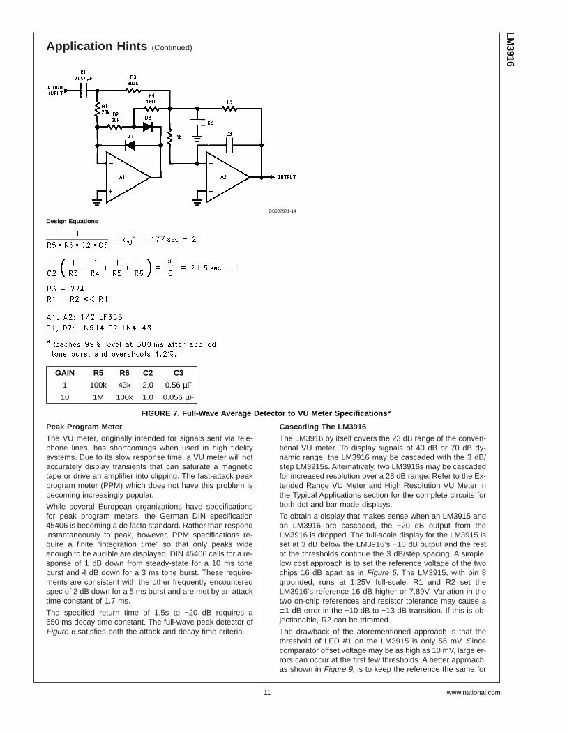
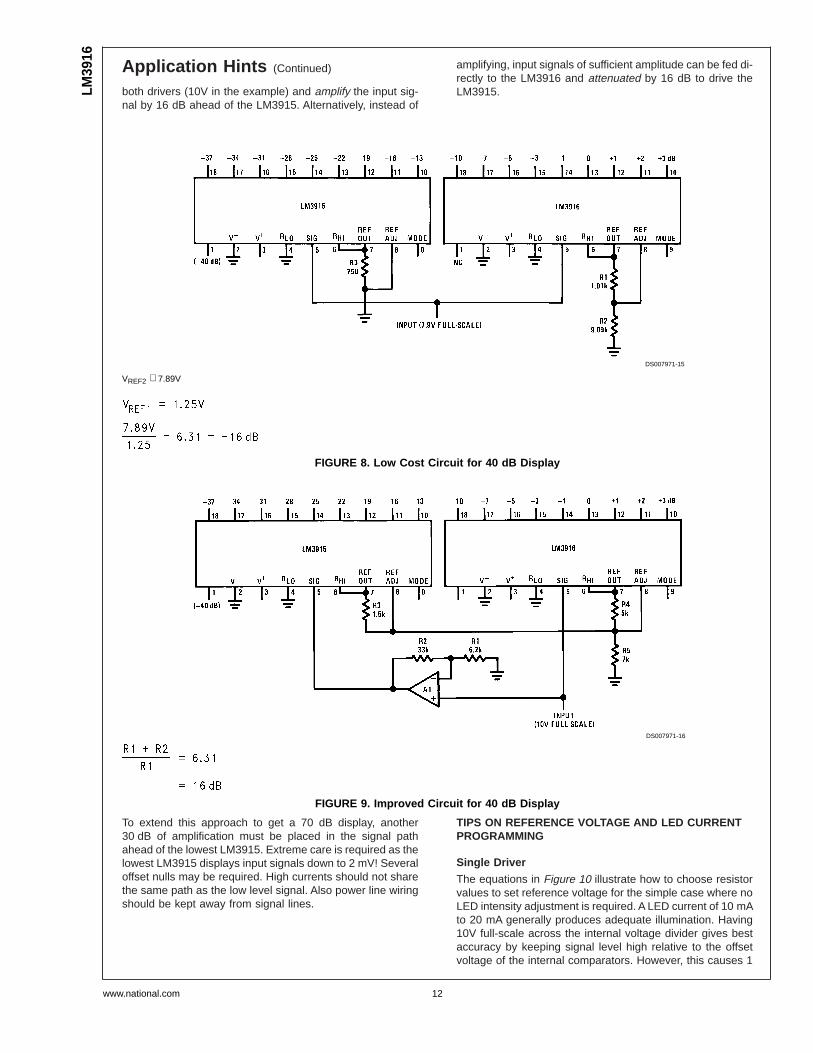
For precision full-wave averaging use the circuit in Figure 5.Using 1% resistors for R1 through R4, gain for positive andnegative signal differs by only 0.5 dB worst case. Substitut-ing 5% resistors increases this to 2 dB worst case. (A 2 dBgain difference means that the display may have a ±1 dB er-ror when the input is a nonsymmetrical transient). The aver-aging time constant is R5•C2. A simple modification resultsin the precision full-wave detector of Figure 6. Since the filtercapacitor is not buffered, this circuit can drive only high im-pedance loads such as the input of an LM3916.
AUDIO METER STANDARDS
VU Meter
The audio level meter most frequently encountered is the VUmeter. Its characteristics are defined as the ANSI specifica-tion C165. The LM3916’s outputs correspond to the meterindications specified with the omission of the −2 VU indica-tion. The VU scale divisions differ slightly from a linear scalein order to obtain whole numbers in dB.
Some of the most important specifications for an AC meterare its dynamic characteristics. These define how the meterresponds to transients and how fast the reading decays. TheVU meter is a relatively slow full-wave averaging type, speci-fied to reach 99% deflection in 300 ms and overshoot by 1 to1.5%. In engineering terms this means a slightly under-damped second order response with a resonant frequencyof 2.1 Hz and a Q of 0.62. Figure 7 depicts a simple rectifier/filter circuit that meets these criteria.
DS007971-11
D1, D2: 1N914 or 1N4148
Average Peak
R2 1k 100k
R3 100k 1k
R1 = R2 for AV = 1R1 = R2/10 for AV = 10C1 = 10/R1
FIGURE 4. Precision Half-Wave Rectifier
DS007971-12
D1, D2: 1N914 or 1N4148
FIGURE 5. Precision Full-Wave Average Detector
DS007971-13
D1, D2, D3, D4: 1N914 OR 1N4148Attack and decay time to DIN PPM spec. Response down 1 dB for 10 mstone burst. Decays 20 dB in 1.5s.
FIGURE 6. Precision Full-Wave Peak Detector
LM39
16
www.national.com 10
Application Hints (Continued)
Peak Program Meter
The VU meter, originally intended for signals sent via tele-phone lines, has shortcomings when used in high fidelitysystems. Due to its slow response time, a VU meter will notaccurately display transients that can saturate a magnetictape or drive an amplifier into clipping. The fast-attack peakprogram meter (PPM) which does not have this problem isbecoming increasingly popular.
While several European organizations have specificationsfor peak program meters, the German DIN specification45406 is becoming a de facto standard. Rather than respondinstantaneously to peak, however, PPM specifications re-quire a finite “integration time” so that only peaks wideenough to be audible are displayed. DIN 45406 calls for a re-sponse of 1 dB down from steady-state for a 10 ms toneburst and 4 dB down for a 3 ms tone burst. These require-ments are consistent with the other frequently encounteredspec of 2 dB down for a 5 ms burst and are met by an attacktime constant of 1.7 ms.
The specified return time of 1.5s to −20 dB requires a650 ms decay time constant. The full-wave peak detector ofFigure 6 satisfies both the attack and decay time criteria.
Cascading The LM3916
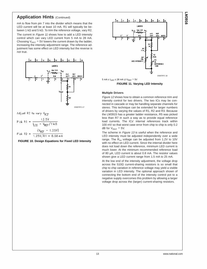
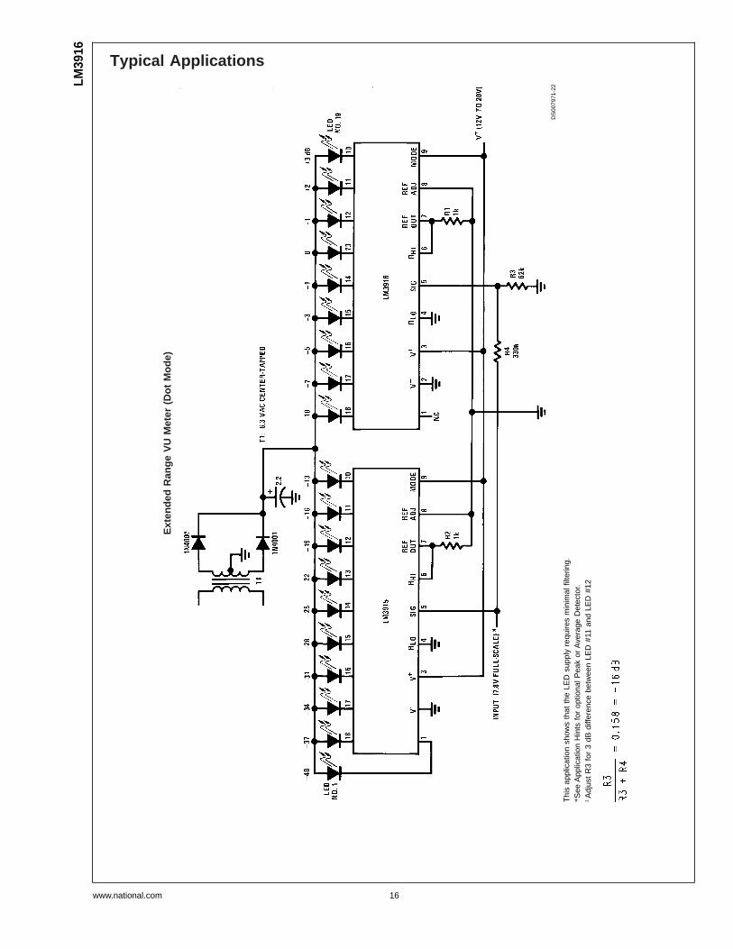
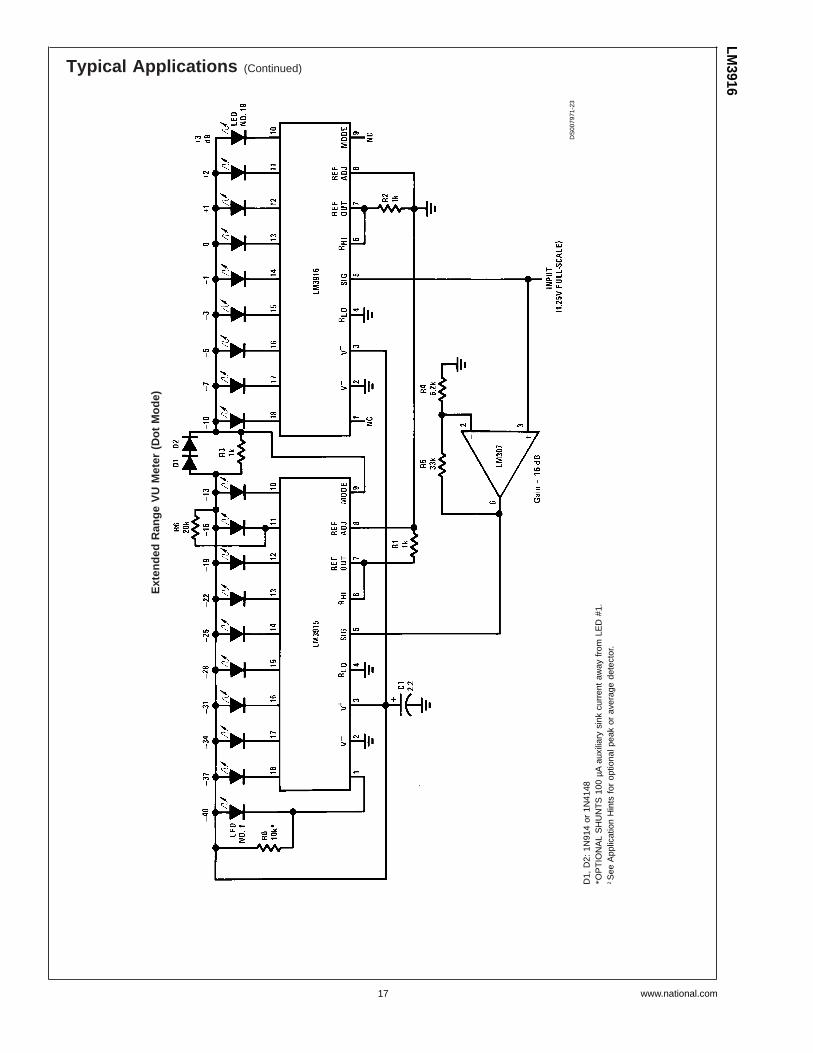
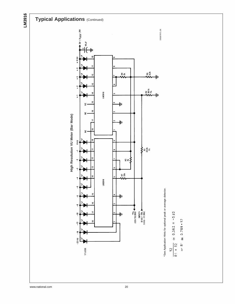
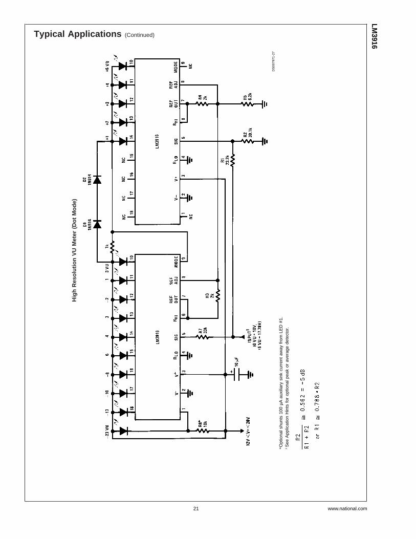
The LM3916 by itself covers the 23 dB range of the conven-tional VU meter. To display signals of 40 dB or 70 dB dy-namic range, the LM3916 may be cascaded with the 3 dB/step LM3915s. Alternatively, two LM3916s may be cascadedfor increased resolution over a 28 dB range. Refer to the Ex-tended Range VU Meter and High Resolution VU Meter inthe Typical Applications section for the complete circuits forboth dot and bar mode displays.
To obtain a display that makes sense when an LM3915 andan LM3916 are cascaded, the −20 dB output from theLM3916 is dropped. The full-scale display for the LM3915 isset at 3 dB below the LM3916’s −10 dB output and the restof the thresholds continue the 3 dB/step spacing. A simple,low cost approach is to set the reference voltage of the twochips 16 dB apart as in Figure 5. The LM3915, with pin 8grounded, runs at 1.25V full-scale. R1 and R2 set theLM3916’s reference 16 dB higher or 7.89V. Variation in thetwo on-chip references and resistor tolerance may cause a±1 dB error in the −10 dB to −13 dB transition. If this is ob-jectionable, R2 can be trimmed.
The drawback of the aforementioned approach is that thethreshold of LED #1 on the LM3915 is only 56 mV. Sincecomparator offset voltage may be as high as 10 mV, large er-rors can occur at the first few thresholds. A better approach,as shown in Figure 9, is to keep the reference the same for
DS007971-14
Design Equations
GAIN R5 R6 C2 C3
1 100k 43k 2.0 0.56 µF
10 1M 100k 1.0 0.056 µF
FIGURE 7. Full-Wave Average Detector to VU Meter Specifications *
LM3916
www.national.com11
Application Hints (Continued)
both drivers (10V in the example) and amplify the input sig-nal by 16 dB ahead of the LM3915. Alternatively, instead of
amplifying, input signals of sufficient amplitude can be fed di-rectly to the LM3916 and attenuated by 16 dB to drive theLM3915.
To extend this approach to get a 70 dB display, another30 dB of amplification must be placed in the signal pathahead of the lowest LM3915. Extreme care is required as thelowest LM3915 displays input signals down to 2 mV! Severaloffset nulls may be required. High currents should not sharethe same path as the low level signal. Also power line wiringshould be kept away from signal lines.
TIPS ON REFERENCE VOLTAGE AND LED CURRENTPROGRAMMING
Single Driver
The equations in Figure 10 illustrate how to choose resistorvalues to set reference voltage for the simple case where noLED intensity adjustment is required. A LED current of 10 mAto 20 mA generally produces adequate illumination. Having10V full-scale across the internal voltage divider gives bestaccuracy by keeping signal level high relative to the offsetvoltage of the internal comparators. However, this causes 1
DS007971-15
VREF2 ≅ 7.89V
FIGURE 8. Low Cost Circuit for 40 dB Display
DS007971-16
FIGURE 9. Improved Circuit for 40 dB Display
LM39
16
www.national.com 12
Application Hints (Continued)
mA to flow from pin 7 into the divider which means that theLED current will be at least 10 mA. R1 will typically be be-tween 1 kΩ and 5 kΩ. To trim the reference voltage, vary R2.
The current in Figure 11 shows how to add a LED intensitycontrol which can vary LED current from 5 mA to 28 mA.Choosing VREF = 5V lowers the current drawn by the ladder,increasing the intensity adjustment range. The reference ad-justment has some effect on LED intensity but the reverse isnot true.
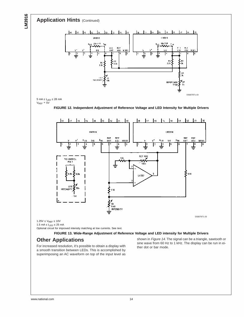
Multiple Drivers
Figure 12 shows how to obtain a common reference trim andintensity control for two drivers. The two ICs may be con-nected in cascade or may be handling separate channels forstereo. This technique can be extended for larger numbersof drivers by varying the values of R1, R2 and R3. Becausethe LM3915 has a greater ladder resistance, R5 was pickedless than R7 in such a way as to provide equal referenceload currents. The ICs’ internal references track within100 mV so that worst case error from chip to chip is only 0.2dB for VREF = 5V.
The scheme in Figure 13 is useful when the reference andLED intensity must be adjusted independently over a widerange. The RHI voltage can be adjusted from 1.2V to 10Vwith no effect on LED current. Since the internal divider heredoes not load down the reference, minimum LED current ismuch lower. At the minimum recommended reference loadof 80 µA, LED current is about 0.8 mA. The resistor valuesshown give a LED current range from 1.5 mA to 25 mA.
At the low end of the intensity adjustment, the voltage dropacross the 510Ω current-sharing resistors is so small thatchip to chip variation in reference voltage may yield a visiblevariation in LED intensity. The optional approach shown ofconnecting the bottom end of the intensity control pot to anegative supply overcomes this problem by allowing a largervoltage drop across the (larger) current-sharing resistors.
DS007971-17
FIGURE 10. Design Equations for Fixed LED Intensity
DS007971-18
5 mA ≤ ILED ≤ 28 mA @ VREF = 5V
FIGURE 11. Varying LED Intensity
LM3916
www.national.com13
Application Hints (Continued)
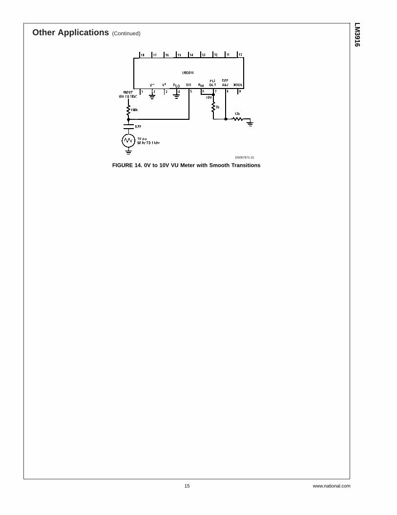
Other ApplicationsFor increased resolution, it’s possible to obtain a display witha smooth transition between LEDs. This is accomplished bysuperimposing an AC waveform on top of the input level as
shown in Figure 14. The signal can be a triangle, sawtooth orsine wave from 60 Hz to 1 kHz. The display can be run in ei-ther dot or bar mode.
DS007971-19
5 mA ≤ ILED ≤ 28 mAVREF = 5V
FIGURE 12. Independent Adjustment of Reference Voltage and LED Intensity for Multiple Drivers
DS007971-20
1.25V ≤ VREF ≤ 10V1.5 mA ≤ ILED ≤ 25 mAOptional circuit for improved intensity matching at low currents. See text.
FIGURE 13. Wide-Range Adjustment of Reference Voltage and LED intensity for Multiple Drivers
LM39
16
www.national.com 14
Other Applications (Continued)
DS007971-21
FIGURE 14. 0V to 10V VU Meter with Smooth Transitions
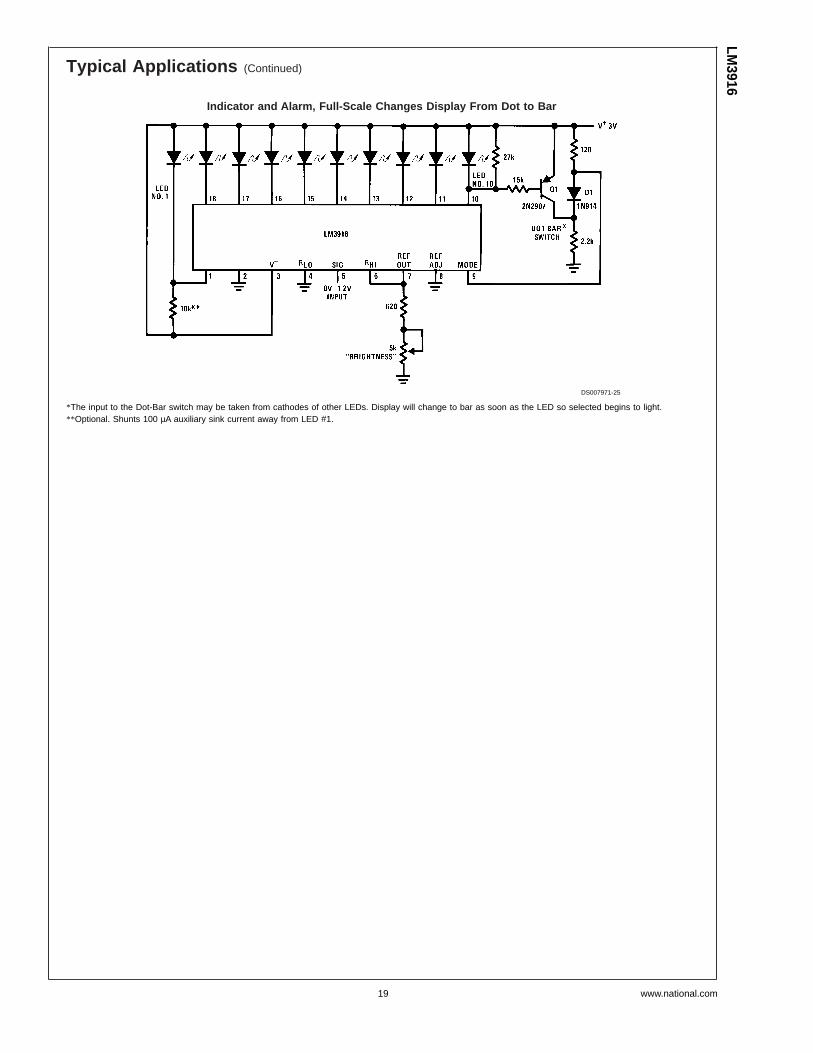
Indicator and Alarm, Full-Scale Changes Display From Dot to Bar
DS007971-25
*The input to the Dot-Bar switch may be taken from cathodes of other LEDs. Display will change to bar as soon as the LED so selected begins to light.**Optional. Shunts 100 µA auxiliary sink current away from LED #1.
LM3916
www.national.com19
Typical Applications (Continued)
Hig
hR
esol
utio
nV
UM
eter
(Bar
Mod
e)
DS
0079
71-2
6
* See
App
licat
ion
Hin
tsfo
rop
tiona
lpea
kor
aver
age
dete
ctor
.
LM39
16
www.national.com 20
Typical Applications (Continued)
Hig
hR
esol
utio
nV
UM
eter
(Dot
Mod
e)
DS
0079
71-2
7
* Opt
iona
lshu
nts
100
µAau
xilia
rysi
nkcu
rren
taw
ayfr
omLE
D# 1
.† S
eeA
pplic
atio
nH
ints
for
optio
nalp
eak
orav
erag
ede
tect
or.
LM3916
www.national.com21
Typical Applications (Continued)
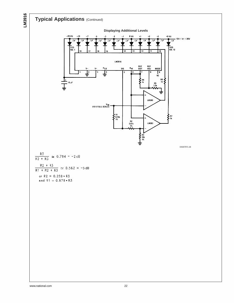
Displaying Additional Levels
DS007971-28
LM39
16
www.national.com 22
Typical Applications (Continued)
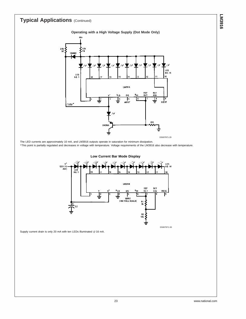
Operating with a High Voltage Supply (Dot Mode Only)
DS007971-29
The LED currents are approximately 10 mA, and LM3916 outputs operate in saturation for minimum dissipation.*This point is partially regulated and decreases in voltage with temperature. Voltage requirements of the LM3916 also decrease with temperature.
Low Current Bar Mode Display
DS007971-30
Supply current drain is only 20 mA with ten LEDs illuminated @ 16 mA.
LM3916
www.national.com23
Typical Applications (Continued)
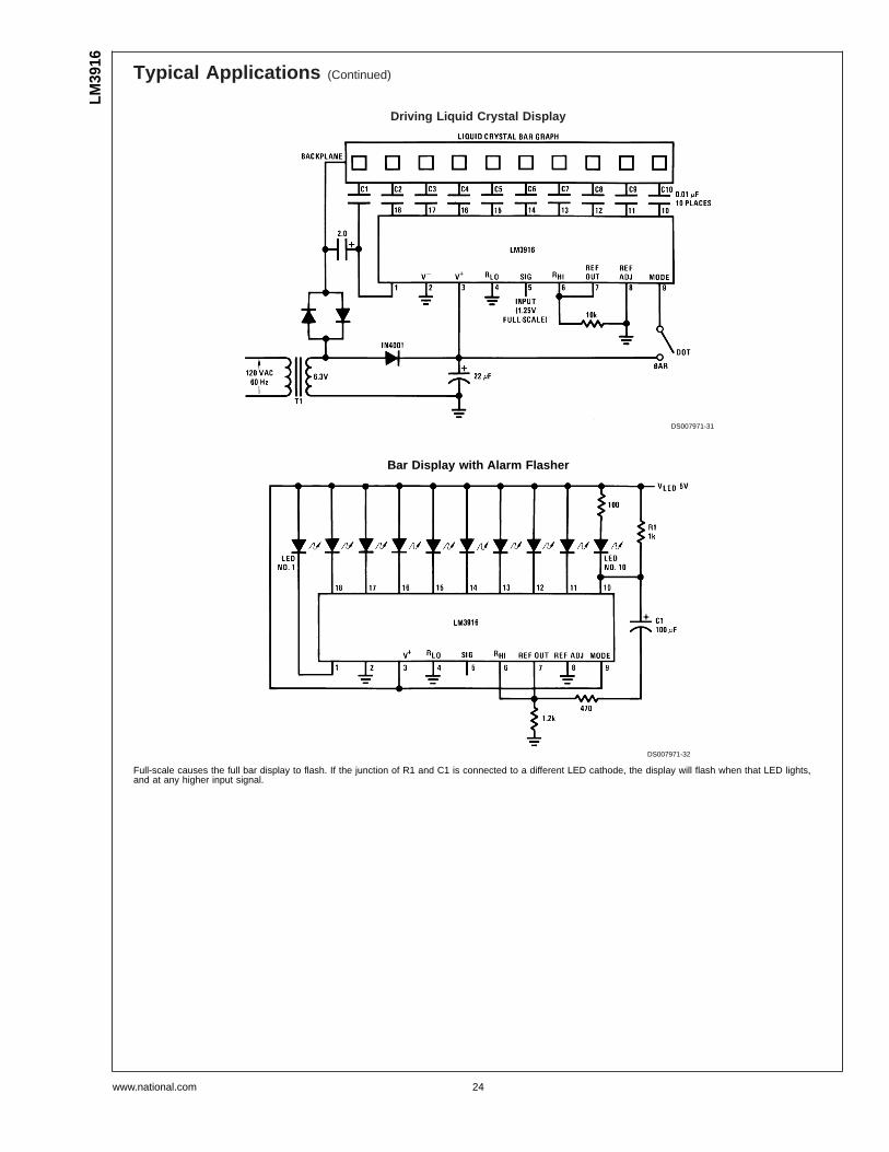
Driving Liquid Crystal Display
DS007971-31
Bar Display with Alarm Flasher
DS007971-32
Full-scale causes the full bar display to flash. If the junction of R1 and C1 is connected to a different LED cathode, the display will flash when that LED lights,and at any higher input signal.
LM39
16
www.national.com 24
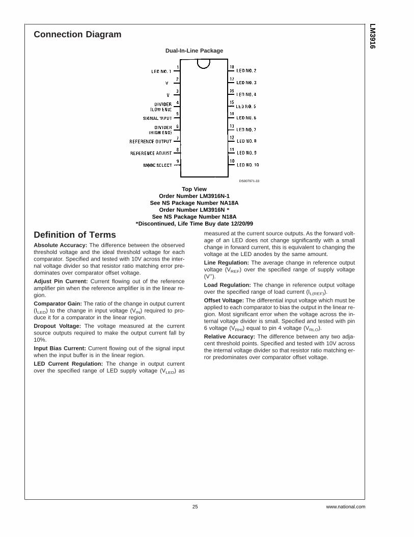
Connection Diagram
Definition of TermsAbsolute Accuracy: The difference between the observedthreshold voltage and the ideal threshold voltage for eachcomparator. Specified and tested with 10V across the inter-nal voltage divider so that resistor ratio matching error pre-dominates over comparator offset voltage.
Adjust Pin Current: Current flowing out of the referenceamplifier pin when the reference amplifier is in the linear re-gion.
Comparator Gain: The ratio of the change in output current(ILED) to the change in input voltage (VIN) required to pro-duce it for a comparator in the linear region.
Dropout Voltage: The voltage measured at the currentsource outputs required to make the output current fall by10%.
Input Bias Current: Current flowing out of the signal inputwhen the input buffer is in the linear region.
LED Current Regulation: The change in output currentover the specified range of LED supply voltage (VLED) as
measured at the current source outputs. As the forward volt-age of an LED does not change significantly with a smallchange in forward current, this is equivalent to changing thevoltage at the LED anodes by the same amount.
Line Regulation: The average change in reference outputvoltage (VREF) over the specified range of supply voltage(V+).
Load Regulation: The change in reference output voltageover the specified range of load current (IL(REF)).
Offset Voltage: The differential input voltage which must beapplied to each comparator to bias the output in the linear re-gion. Most significant error when the voltage across the in-ternal voltage divider is small. Specified and tested with pin6 voltage (VRHI) equal to pin 4 voltage (VRLO).
Relative Accuracy: The difference between any two adja-cent threshold points. Specified and tested with 10V acrossthe internal voltage divider so that resistor ratio matching er-ror predominates over comparator offset voltage.
Dual-In-Line Package
DS007971-33
Top ViewOrder Number LM3916N-1
See NS Package Number NA18AOrder Number LM3916N *
See NS Package Number N18A*Discontinued, Life Time Buy date 12/20/99