PIN Diode Limiter 0.4 - 2.5 GHz Rev. V1 LM501202-L-C-300 MACOM Technology Solutions Inc. (MACOM) and its affiliates reserve the right to make changes to the product(s) or information contained herein without notice. Visit www.macom.com for additional data sheets and product information. For further information and support please visit: https://www.macom.com/support DC-0015215 1 Features Surface Mount Limiter in 8 mm x 5 mm x 2.5 mm Package Incorporates PIN Limiter Diodes DC Blocks & DC Return Higher Peak Power Handling than Plastic: 125 W Higher Average Power Handling than Plastic: 5 W CW Lower Insertion Loss: 0.4 dB Lower Flat Leakage Power: 21 dB RoHS* Compliant Description The LM501202-L-C-300 surface mount silicon PIN diode limiter is manufactured using a proven hybrid manufacturing process incorporating PIN diodes and passive devices integrated within a ceramic substrate. This low profile, compact, surface mount component offers superior low and high signal performance to comparable MMIC devices in QFN packages. The limiter modules are designed to optimize small signal insertion loss, noise figure and high signal flat leakage performance from 0.4 - 2.5 GHz. Using PIN diodes with lower thermal resistance (<70°C/W), RF CW incident power levels of 37 dBm and RF peak incident power levels of 51 dBm @ 1 μs RF pulse width, 0.1% duty cycle are very achievable. In addition, this design concept provides lower flat leakage power (<21 dBm) and lower spike leakage energy (<0.2 Ergs) for superior LNA protection. This LM501202-L-C-300 limiters are ideal for receiver protection in octave band radar applications, requiring high volume, surface mount, solder re-flow manufacturing. These products are durable, reliable, and capable of meeting all military, commercial, and industrial environments. The devices are fully RoHS compliant and are available in tube or tape-reel. * Restrictions on Hazardous Substances, European Union Directive 2011/65/EU. Limiter Schematic Ordering Information Part Number Package LM501202-L-C-300-T tube packaging LM501202-L-C-300-R 250 or 500 piece reel LM501202-L-C-300-W waffle packaging LM501202-L-C-300-E RF evaluation board Pin Out
Transcript
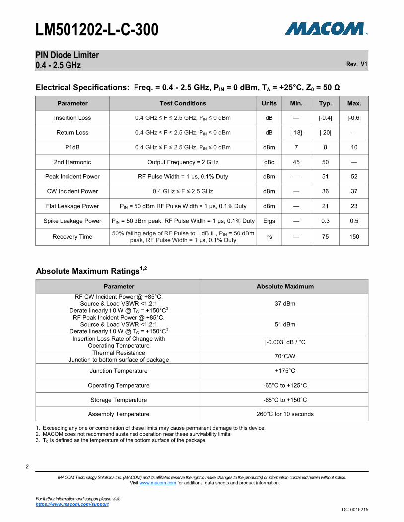
PIN Diode Limiter 0.4 - 2.5 GHz
Rev. V1
LM501202-L-C-300
1 1
MACOM Technology Solutions Inc. (MACOM) and its affiliates reserve the right to make changes to the product(s) or information contained herein without notice. Visit www.macom.com for additional data sheets and product information.
For further information and support please visit: https://www.macom.com/support
DC-0015215
1
Features
Surface Mount Limiter in 8 mm x 5 mm x 2.5 mm Package
Incorporates PIN Limiter Diodes
DC Blocks & DC Return
Higher Peak Power Handling than Plastic: 125 W
Higher Average Power Handling than Plastic: 5 W CW
Lower Insertion Loss: 0.4 dB
Lower Flat Leakage Power: 21 dB
RoHS* Compliant
Description
The LM501202-L-C-300 surface mount silicon PIN diode limiter is manufactured using a proven hybrid manufacturing process incorporating PIN diodes and passive devices integrated within a ceramic substrate. This low profile, compact, surface mount component offers superior low and high signal performance to comparable MMIC devices in QFN packages. The limiter modules are designed to optimize small signal insertion loss, noise figure and high signal flat leakage performance from 0.4 - 2.5 GHz. Using PIN diodes with lower thermal resistance (<70°C/W), RF CW incident power levels of 37 dBm and RF peak incident power levels of 51 dBm @ 1 μs RF pulse width, 0.1% duty cycle are very achievable. In addition, this design concept provides lower flat leakage power (<21 dBm) and lower spike leakage energy (<0.2 Ergs) for superior LNA protection. This LM501202-L-C-300 limiters are ideal for receiver protection in octave band radar applications, requiring high volume, surface mount, solder re-flow manufacturing. These products are durable, reliable, and capable of meeting all military, commercial, and industrial environments. The devices are fully RoHS compliant and are available in tube or tape-reel.
* Restrictions on Hazardous Substances, European Union Directive 2011/65/EU.
MACOM Technology Solutions Inc. (MACOM) and its affiliates reserve the right to make changes to the product(s) or information contained herein without notice. Visit www.macom.com for additional data sheets and product information.
For further information and support please visit: https://www.macom.com/support
Insertion Loss Rate of Change with Operating Temperature
|-0.003| dB / °C
Thermal Resistance Junction to bottom surface of package
70°C/W
Junction Temperature +175°C
Operating Temperature -65°C to +125°C
Storage Temperature -65°C to +150°C
Assembly Temperature 260°C for 10 seconds
1. Exceeding any one or combination of these limits may cause permanent damage to this device. 2. MACOM does not recommend sustained operation near these survivability limits. 3. TC is defined as the temperature of the bottom surface of the package.
MACOM Technology Solutions Inc. (MACOM) and its affiliates reserve the right to make changes to the product(s) or information contained herein without notice. Visit www.macom.com for additional data sheets and product information.
For further information and support please visit: https://www.macom.com/support
DC-0015215
3
Typical Performance Curves
Insertion Loss vs. Frequency Return Loss vs. Frequency
MACOM Technology Solutions Inc. (MACOM) and its affiliates reserve the right to make changes to the product(s) or information contained herein without notice. Visit www.macom.com for additional data sheets and product information.
For further information and support please visit: https://www.macom.com/support
DC-0015215
4
Handling Procedures
Please observe the following precautions to avoid damage:
Static and Moisture Sensitivity
These electronic devices are sensitive to electrostatic discharge (ESD) and can be damaged by static electricity. Proper ESD control techniques should be used when handling these Class 0 (HBM) devices. The moisture sensitivity level rating for this device is MSL 2.
Environmental Capabilities
This limiter is capable of meeting the environmental requirements of MIL-STD-750 and MIL-STD-202.
Assembly Instructions
LM501202-L-C‐300 may be placed onto circuit boards with pick and place manufacturing equipment from tube or tape-reel dispensing. The devices are attached to the circuit board using conventional solder re-flow or wave soldering procedures with RoHS type or Sn63/Pb37 type solders per Table 1 and Graph 1 Time-Temperature recommended profile.
RF Circuit Solder Footprint, case style 300 (CS300)
Recommended RF circuit is Rogers R04350B, 10 mils thick. The hatched metal area on circuit side of device is RF, DC and thermal grounded. Vias should be solid copper fill and gold plated for optimum heat transfer from backside of switch module through circuit vias to metal thermal ground.
MACOM Technology Solutions Inc. (MACOM) and its affiliates reserve the right to make changes to the product(s) or information contained herein without notice. Visit www.macom.com for additional data sheets and product information.
For further information and support please visit: https://www.macom.com/support
DC-0015215
5
Criteria for Proper Mounting on PCB
When a large signal is incident upon the input of the LM501202-L-C-300, the impedance of the coarse limiter diodes is forced to a low value by the charge which is injected into these diodes by the combination of the current from the internal detector stage and the large RF voltage initially present across these diodes. As the impedance of these diodes decreases, an increasingly large impedance mismatch with the impedance of the transmission line to which the limiter is connected is created. Ultimately, the impedance of the coarse limiter diodes is reduced to a few ohms or less. This mismatch creates a standing wave, with a current maximum and voltage minimum located at the position of the coarse limiter diodes. While the large majority of the input signal power is reflected back to its source due to the impedance mismatch, the significant RF current that flows at the current maximum causes Joule heating to occur in the coarse limiter diodes. In order to maintain the junction temperature of these diodes below their maximum rated value, there must be a path with minimal thermal resistance from the coarse diodes to the external system heat sink. Also, there must be a minimal electrical resistance and inductance between the underside of the limiter module package and the system ground in order to achieve maximum RF isolation between the input and the output of the limiter module.
For these reasons, it is imperative that there are no voids in the electrical and thermal paths directly under the coarse limiter diodes. Care must be taken when mounting the LM501202-L-C-300 to avoid voids in the solder joint in the area along the lengthwise axis of the package, under and between the filled vias in the AlN substrate of the module which are shown in the diagram (above). It is also important to ensure no solder voids exist between the limiter module RF ports and the PCB to which the limiter module is attached. No greater than 50% of the remaining metalized area on the bottom of the package may contain solder voids.
MACOM Technology Solutions Inc. (MACOM) and its affiliates reserve the right to make changes to the product(s) or information contained herein without notice. Visit www.macom.com for additional data sheets and product information.
For further information and support please visit: https://www.macom.com/support
DC-0015215
6
The evaluation board for the LM501202-L-C-300 limiter is shown above. This evaluation board comprises two sections: the evaluation circuit for the limiter module; and, a reference transmission line. The limiter module is mounted in position U1. Its RF input is connected to J1 and its output port is connected to J2, via two 50-Ω microstrip transmission lines. The reference path 50-Ω microstrip transmission line structure can be utilized to determine the insertion loss of the transmission line structures between the limiter module output and J2, so that their respective insertion losses may be subtracted from the total insertion loss measured between J1 and J2. This enables the resolution of the insertion loss of the limiter module only. The evaluation board is supplied mounted on a heat sink. The maximum RF input power specified in the Absolute Maximum Ratings table must not be exceeded.
MACOM Technology Solutions Inc. (MACOM) and its affiliates reserve the right to make changes to the product(s) or information contained herein without notice. Visit www.macom.com for additional data sheets and product information.
For further information and support please visit: https://www.macom.com/support
DC-0015215
8
The hatched metal area on circuit side of device is RF, DC and thermal grounded. Dimensions are in inches (mm) Substrate Material: 20 mil thick Alumina Nitride (ALN) RF Cover: Black Ceramic Top Side and Backside Metallization: 100 µ IN. typical plated over Ti-Pd.
MACOM Technology Solutions Inc. (MACOM) and its affiliates reserve the right to make changes to the product(s) or information contained herein without notice. Visit www.macom.com for additional data sheets and product information.
For further information and support please visit: https://www.macom.com/support
DC-0015215
9
MACOM Technology Solutions Inc. All rights reserved. Information in this document is provided in connection with MACOM Technology Solutions Inc ("MACOM")products. These materials are provided by MACOM as a service to its customers and may be used for informational purposes only. Except as provided in MACOM's Terms and Conditions of Sale for such products or in any separate agreement related to this document, MACOM assumes no liability whatsoever. MACOM assumes no responsibility for errors or omissions in these materials. MACOM may make changes to specifications and product descriptions at any time, without notice. MACOM makes no commitment to update the information and shall have no responsibility whatsoever for conflicts or incompatibilities arising from future changes to its specifications and product descriptions. No license, express or implied, by estoppels or otherwise, to any intellectual property rights is granted by this document. THESE MATERIALS ARE PROVIDED "AS IS" WITHOUT WARRANTY OF ANY KIND, EITHER EXPRESS OR IMPLIED, RELATING TO SALE AND/OR USE OF MACOM PRODUCTS INCLUDING LIABILITY OR WARRANTIES RELATING TO FITNESS FOR A PARTICULAR PURPOSE, CONSEQUENTIAL OR INCIDENTAL DAMAGES, MERCHANTABILITY, OR INFRINGEMENT OF ANY PATENT, COPYRIGHT OR OTHER INTELLECTUAL PROPERTY RIGHT. MACOM FURTHER DOES NOT WARRANT THE ACCURACY OR COMPLETENESS OF THE INFORMATION, TEXT, GRAPHICS OR OTHER ITEMS CONTAINED WITHIN THESE MATERIALS. MACOM SHALL NOT BE LIABLE FOR ANY SPECIAL, INDIRECT, INCIDENTAL, OR CONSEQUENTIAL DAMAGES, INCLUDING WITHOUT LIMITATION, LOST REVENUES OR LOST PROFITS, WHICH MAY RESULT FROM THE USE OF THESE MATERIALS. MACOM products are not intended for use in medical, lifesaving or life sustaining applications. MACOM customers using or selling MACOM products for use in such applications do so at their own risk and agree to fully indemnify MACOM for any damages resulting from such improper use or sale.