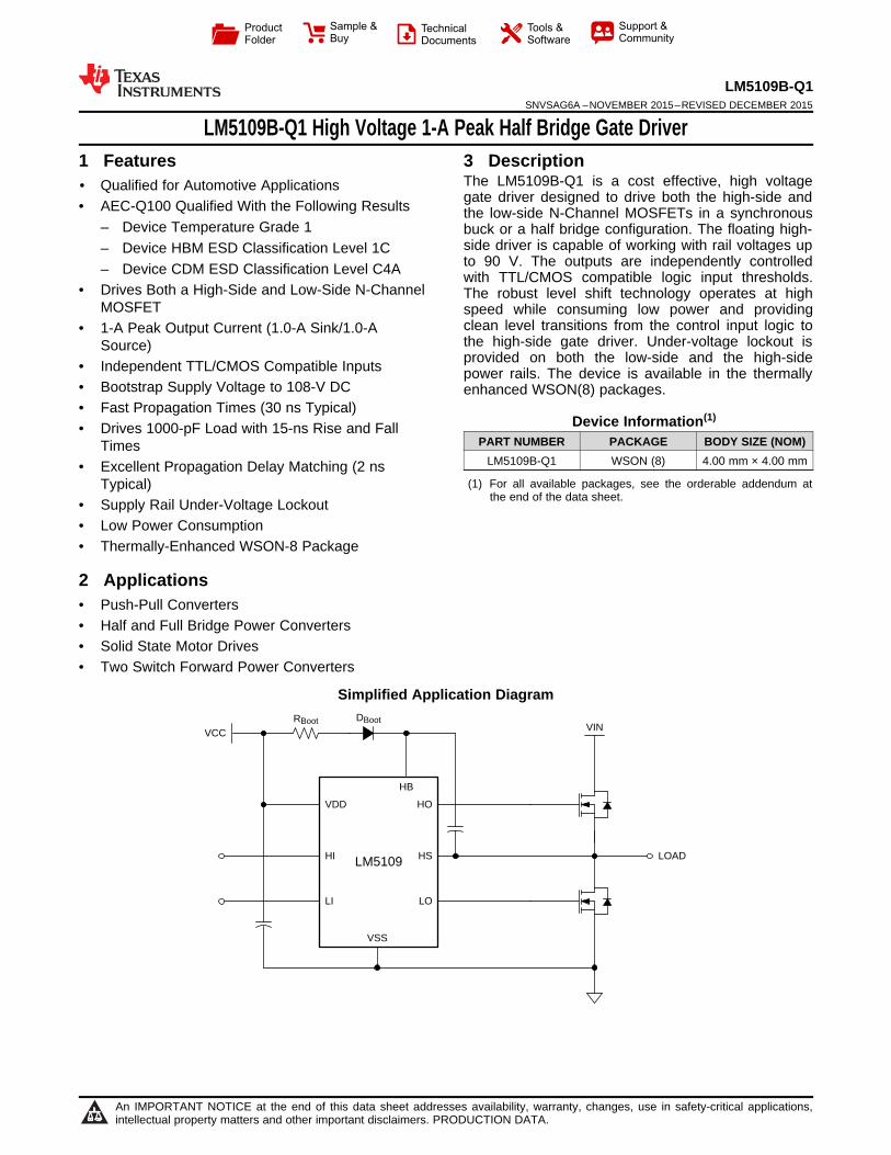
LM5109 VIN VCC VDD HI LI VSS HS LO HO HB R Boot D Boot LOAD Product Folder Sample & Buy Technical Documents Tools & Software Support & Community LM5109B-Q1 SNVSAG6A – NOVEMBER 2015 – REVISED DECEMBER 2015 LM5109B-Q1 High Voltage 1-A Peak Half Bridge Gate Driver 1 Features 3 Description The LM5109B-Q1 is a cost effective, high voltage 1• Qualified for Automotive Applications gate driver designed to drive both the high-side and • AEC-Q100 Qualified With the Following Results the low-side N-Channel MOSFETs in a synchronous – Device Temperature Grade 1 buck or a half bridge configuration. The floating high- side driver is capable of working with rail voltages up – Device HBM ESD Classification Level 1C to 90 V. The outputs are independently controlled – Device CDM ESD Classification Level C4A with TTL/CMOS compatible logic input thresholds. • Drives Both a High-Side and Low-Side N-Channel The robust level shift technology operates at high MOSFET speed while consuming low power and providing clean level transitions from the control input logic to • 1-A Peak Output Current (1.0-A Sink/1.0-A the high-side gate driver. Under-voltage lockout is Source) provided on both the low-side and the high-side • Independent TTL/CMOS Compatible Inputs power rails. The device is available in the thermally • Bootstrap Supply Voltage to 108-V DC enhanced WSON(8) packages. • Fast Propagation Times (30 ns Typical) Device Information (1) • Drives 1000-pF Load with 15-ns Rise and Fall PART NUMBER PACKAGE BODY SIZE (NOM) Times LM5109B-Q1 WSON (8) 4.00 mm × 4.00 mm • Excellent Propagation Delay Matching (2 ns (1) For all available packages, see the orderable addendum at Typical) the end of the data sheet. • Supply Rail Under-Voltage Lockout • Low Power Consumption • Thermally-Enhanced WSON-8 Package 2 Applications • Push-Pull Converters • Half and Full Bridge Power Converters • Solid State Motor Drives • Two Switch Forward Power Converters Simplified Application Diagram 1 An IMPORTANT NOTICE at the end of this data sheet addresses availability, warranty, changes, use in safety-critical applications, intellectual property matters and other important disclaimers. PRODUCTION DATA.
Transcript
LM5109
VINVCC
VDD
HI
LI
VSS
HS
LO
HO
HB
RBoot DBoot
LOAD
Product
Folder
Sample &Buy
Technical
Documents
Tools &
Software
Support &Community
LM5109B-Q1SNVSAG6A –NOVEMBER 2015–REVISED DECEMBER 2015
LM5109B-Q1 High Voltage 1-A Peak Half Bridge Gate Driver1 Features 3 Description
The LM5109B-Q1 is a cost effective, high voltage1• Qualified for Automotive Applications
gate driver designed to drive both the high-side and• AEC-Q100 Qualified With the Following Results the low-side N-Channel MOSFETs in a synchronous– Device Temperature Grade 1 buck or a half bridge configuration. The floating high-
side driver is capable of working with rail voltages up– Device HBM ESD Classification Level 1Cto 90 V. The outputs are independently controlled– Device CDM ESD Classification Level C4A with TTL/CMOS compatible logic input thresholds.
• Drives Both a High-Side and Low-Side N-Channel The robust level shift technology operates at highMOSFET speed while consuming low power and providing
clean level transitions from the control input logic to• 1-A Peak Output Current (1.0-A Sink/1.0-Athe high-side gate driver. Under-voltage lockout isSource)provided on both the low-side and the high-side• Independent TTL/CMOS Compatible Inputs power rails. The device is available in the thermally
• Bootstrap Supply Voltage to 108-V DC enhanced WSON(8) packages.• Fast Propagation Times (30 ns Typical)
Device Information(1)• Drives 1000-pF Load with 15-ns Rise and Fall
PART NUMBER PACKAGE BODY SIZE (NOM)TimesLM5109B-Q1 WSON (8) 4.00 mm × 4.00 mm• Excellent Propagation Delay Matching (2 ns
(1) For all available packages, see the orderable addendum atTypical)the end of the data sheet.• Supply Rail Under-Voltage Lockout
• Low Power Consumption• Thermally-Enhanced WSON-8 Package
2 Applications• Push-Pull Converters• Half and Full Bridge Power Converters• Solid State Motor Drives• Two Switch Forward Power Converters
Simplified Application Diagram
1
An IMPORTANT NOTICE at the end of this data sheet addresses availability, warranty, changes, use in safety-critical applications,intellectual property matters and other important disclaimers. PRODUCTION DATA.
LM5109B-Q1www.ti.com SNVSAG6A –NOVEMBER 2015–REVISED DECEMBER 2015
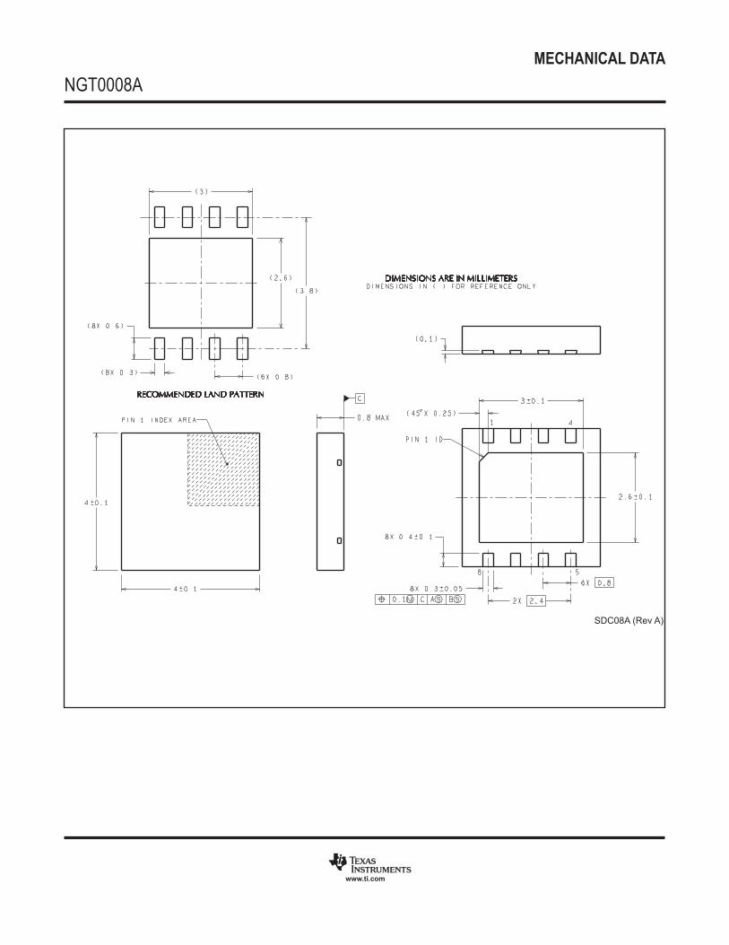
5 Pin Configuration and Functions
NGT Package8-Pin WSON
Top View
Pin FunctionsPIN
I/O (1) DESCRIPTION APPLICATIONS INFORMATIONNO. (2) NAME
Locally decouple to VSS using low ESR/ESL capacitor located as close1 VDD P Positive gate drive supply to IC as possible.The HI input is TTL/CMOS Compatible input thresholds. Unused HI2 HI I High side control input input should be tied to ground and not left open.The LI input is TTL/CMOS Compatible input thresholds. Unused LI3 LI I Low side control input input should be tied to ground and not left open.
4 VSS G Ground reference All signals are referenced to this ground.Low side gate driver5 LO O Connect to the gate of the low-side N-MOS device.outputHigh side source Connect to the negative terminal of the bootstrap capacitor and to the6 HS P connection source of the high-side N-MOS device.High side gate driver7 HO O Connect to the gate of the high-side N-MOS device.output
Connect the positive terminal of the bootstrap capacitor to HB and theHigh side gate driver8 HB P negative terminal of the bootstrap capacitor to HS. The bootstrappositive supply rail capacitor should be placed as close to IC as possible.
(1) P = Power, G = Ground, I = Input, O = Output, I/O = Input/Output(2) For WSON-8 package, it is recommended that the exposed pad on the bottom of the package be soldered to ground plane on the PCB
and the ground plane should extend out from underneath the package to improve heat dissipation.
LM5109B-Q1SNVSAG6A –NOVEMBER 2015–REVISED DECEMBER 2015 www.ti.com
6 Specifications
6.1 Absolute Maximum Ratingsover operating free-air temperature range (unless otherwise noted) (1)
MIN MAX UNITVDD to VSS –0.3 18 VHB to HS –0.3 18 VLI or HI to VSS –0.3 VDD + 0.3 VLO to VSS –0.3 VDD + 0.3 VHO to VSS VHS – 0.3 VHB + 0.3 VHS to VSS
(2) –5 90 VHB to VSS 108 VJunction temperature –40 150 °CStorage temperature, Tstg –55 150 °C
(1) Stresses beyond those listed under Absolute Maximum Ratings may cause permanent damage to the device. These are stress ratingsonly, which do not imply functional operation of the device at these or any other conditions beyond those indicated under RecommendedOperating Conditions. Exposure to absolute-maximum-rated conditions for extended periods may affect device reliability.
(2) In the application, the HS node is clamped by the body diode of the external lower N-MOSFET, therefore the HS voltage will generallynot exceed –1 V. However in some applications, board resistance and inductance may result in the HS node exceeding this statedvoltage transiently. If negative transients occur on HS, the HS voltage must never be more negative than VDD – 15 V. For example, ifVDD = 10 V, the negative transients at HS must not exceed –5 V.
6.2 ESD RatingsVALUE UNIT
Human-body model (HBM), per AEC Q100-002 (1) 1500V(ESD) Electrostatic discharge V
Charged-device model (CDM), per AEC Q100-011 750
(1) AEC Q100-002 indicates that HBM stressing shall be in accordance with the ANSI/ESDA/JEDEC JS-001 specification.
6.3 Recommended Operating Conditionsover operating free-air temperature range (unless otherwise noted)
MIN NOM MAX UNITVDD 8 14 VHS (1) –1 90 VHB VHS+8 VHS+14 VHS Slew Rate < 50 V/nsJunction Temperature –40 125 °C
(1) In the application, the HS node is clamped by the body diode of the external lower N-MOSFET, therefore the HS voltage will generallynot exceed –1 V. However in some applications, board resistance and inductance may result in the HS node exceeding this statedvoltage transiently. If negative transients occur on HS, the HS voltage must never be more negative than VDD – 15 V. For example, ifVDD = 10 V, the negative transients at HS must not exceed –5 V.
LM5109B-Q1www.ti.com SNVSAG6A –NOVEMBER 2015–REVISED DECEMBER 2015
7 Detailed Description
7.1 OverviewThe LM5109B-Q1 is a cost-effective, high voltage gate driver designed to drive both the high-side and the low-side N-channel FETs in a synchronous buck or a half-bridge configuration. The outputs are independentlycontrolled with TTL/CMOS compatible input thresholds. The floating high-side driver is capable of working withHB voltage up to 108 V. An external high voltage diode must be provided to charge high side gate drivebootstrap capacitor. A robust level shifter operates at high speed while consuming low power and providing cleanlevel transitions from the control logic to the high side gate driver. Under-voltage lockout (UVLO) is provided onboth the low side and the high side power rails.
7.2 Functional Block Diagram
7.3 Feature Description
7.3.1 Start-up and UVLOBoth top and bottom drivers include UVLO protection circuitry which monitors the supply voltage (VDD) andbootstrap capacitor voltage (VHB–HS) independently. The UVLO circuit inhibits each output until sufficient supplyvoltage is available to turn on the external MOSFETs, and the built-in UVLO hysteresis prevents chatteringduring supply voltage variations. When the supply voltage is applied to the VDD pin of the LM5109B-Q1, the topand bottom gates are held low until VDD exceeds the UVLO threshold, typically about 6.7 V. Any UVLO conditionon the bootstrap capacitor (VHB–HS) will only disable the high- side output (HO).
Table 1. VDD UVLO Feature Logic OperationCondition (VHB-HS>VHBR for all case below) HI LI HO LO
VDD-VSS < VDDR during device start-up H L L LVDD-VSS < VDDR during device start-up L H L LVDD-VSS < VDDR during device start-up H H L LVDD-VSS < VDDR during device start-up L L L L
VDD-VSS < VDDR – VDDH after device start-up H L L LVDD-VSS < VDDR – VDDH after device start-up L H L LVDD-VSS < VDDR – VDDH after device start-up H H L LVDD-VSS < VDDR – VDDH after device start-up L L L L
LM5109B-Q1SNVSAG6A –NOVEMBER 2015–REVISED DECEMBER 2015 www.ti.com
Table 2. VHB-HS UVLO Feature Logic OperationCondition (VDD>VDDR for all case below) HI LI HO LO
VHB-HS < VHBR during device start-up H L L LVHB-HS < VHBR during device start-up L H L HVHB-HS < VHBR during device start-up H H L HVHB-HS < VHBR during device start-up L L L L
VHB-HS < VHBR – VHBH after device start-up H L L LVHB-HS < VHBR – VHBH after device start-up L H L HVHB-HS < VHBR – VHBH after device start-up H H L HVHB-HS < VHBR – VHBH after device start-up L L L L
7.3.2 Level ShiftThe level shift circuit is the interface from the high-side input to the high-side driver stage which is referenced tothe switch node (HS). The level shift allows control of the HO output which is referenced to the HS pin andprovides excellent delay matching with the low-side driver.
7.3.3 Output StagesThe output stages are the interface to the power MOSFETs in the power train. High slew rate, low resistance,and high peak current capability of both outputs allow for efficient switching of the power MOSFETs. The low-side output stage is referenced to VSS and the high-side is referenced to HS.
7.4 HS Transient Voltages Below Ground
The HS node will always be clamped by the body diode of the lower external FET. In some situations, boardresistances and inductances can cause the HS node to transiently swing several volts below ground. The HSnode can swing below ground provided:1. HS must always be at a lower potential than HO. Pulling HO more than –0.3 V below HS can activate
parasitic transistors resulting in excessive current flow from the HB supply, possibly resulting in damage tothe IC. The same relationship is true with LO and VSS. If necessary, a Schottky diode can be placedexternally between HO and HS or LO and GND to protect the IC from this type of transient. The diode mustbe placed as close to the IC pins as possible in order to be effective.
2. HB to HS operating voltage should be 15 V or less. Hence, if the HS pin transient voltage is –5 V, VDDshould be ideally limited to 10 V to keep HB to HS below 15 V.
3. Low ESR bypass capacitors from HB to HS and from VDD to VSS are essential for proper operation. Thecapacitor should be located at the leads of the IC to minimize series inductance. The peak currents from LOand HO can be quite large. Any series inductances with the bypass capacitor will cause voltage ringing at theleads of the IC which must be avoided for reliable operation.
7.5 Device Functional ModesThe device operates in normal mode and UVLO mode. See Start-up and UVLO for more information on UVLOoperation mode. In normal mode when the VDD and VHB–HS are above UVLO threshold, the output stage isdependent on the states of the HI and LI pins. The output HO and LO will be low if input state is floating.
Table 3. INPUT/OUTPUT Logic TableHI LI HO (1) LO (2)
L L L LL H L HH L H LH H H H
Floating Floating L L
(1) HO is measured with respect to the HS.(2) LO is measured with respect to the VSS.
LM5109B-Q1www.ti.com SNVSAG6A –NOVEMBER 2015–REVISED DECEMBER 2015
8 Application and Implementation
NOTEInformation in the following applications sections is not part of the TI componentspecification, and TI does not warrant its accuracy or completeness. TI’s customers areresponsible for determining suitability of components for their purposes. Customers shouldvalidate and test their design implementation to confirm system functionality.
8.1 Application InformationTo operate fast switching of power MOSFETs at high switching frequencies and to reduce associated switchinglosses, a powerful gate driver is employed between the PWM output of controller and the gates of the powersemiconductor devices. Also, gate drivers are indispensable when it is impossible for the PWM controller todirectly drive the gates of the switching devices. With the advent of digital power, this situation is oftenencountered because the PWM signal from the digital controller is often a 3.3 V logic signal which cannoteffectively turn on a power switch. Level shift circuit is needed to boost the 3.3 V signal to the gate-drive voltage(such as 12 V) in order to fully turn-on the power device and minimize conduction losses. Traditional buffer drivecircuits based on NPN/PNP bipolar transistors in totem-pole arrangement prove inadequate with digital powerbecause they lack level-shifting capability. Gate drivers effectively combine both the level-shifting and buffer-drivefunctions. Gate drivers also find other needs such as minimizing the effect of high-frequency switching noise (byplacing the high-current driver IC physically close to the power switch), driving gate-drive transformers andcontrolling floating power-device gates, reducing power dissipation and thermal stress in controllers by movinggate charge power losses from the controller into the driver.
The LM5109B-Q1 is the high voltage gate drivers designed to drive both the high-side and low-side N-ChannelMOSFETs in a half-bridge/full bridge configuration or in a synchronous buck circuit. The floating high side driveris capable of operating with supply voltages up to 90V. This allows for N-Channel MOSFETs control in half-bridge, full-bridge, push-pull, two switch forward and active clamp topologies. The outputs are independentlycontrolled. Each channel is controlled by its respective input pins (HI and LI), allowing full and independentflexibility to control ON and OFF state of the output.
8.2 Typical Application
Figure 14. LM5109B-Q1 Driving MOSFETs in a Half Bridge Converter
8.2.2.1 Select Bootstrap and VDD CapacitorThe bootstrap capacitor must maintain the VHB-HS voltage above the UVLO threshold for normal operation.Calculate the maximum allowable drop across the bootstrap capacitor with Equation 1.
where• VDD = Supply voltage of the gate drive IC;• VDH = Bootstrap diode forward voltage drop;• VHBL = VHBRmax – VHBH, HB falling threshold; (1)
Then, the total charge needed per switching cycle could be estimated by Equation 2.
where• QG: Total MOSFET gate charge• IHBS: HB to VSS Leakage current• DMax: Converter maximum duty cycle• IHB: HB Quiescent current (2)
Therefore, the minimum CBoot should be:
(3)
In practice, the value of the CBoot capacitor should be greater than calculated to allow for situations where thepower stage may skip pulse due to load transients. It is recommended to have enough margins and place thebootstrap capacitor as close to the HB and HS pins as possible.
CBoot = 100 nF (4)
As a general rule the local VDD bypass capacitor should be 10 times greater than the value of CBoot, as shown inEquation 5.
CVDD = 1 µF (5)
The bootstrap and bias capacitors should be ceramic types with X7R dielectric. The voltage rating should betwice that of the maximum VDD considering capacitance tolerances once the devices have a DC bias voltageacross them and to ensure long-term reliability.
8.2.2.2 Select External Bootstrap Diode and Its Series ResistorThe bootstrap capacitor is charged by the VDD through the external bootstrap diode every cycle when low sideMOSFET turns on. The charging of the capacitor involves high peak currents, and therefore transient powerdissipation in the bootstrap diode may be significant and the conduction loss also depends on its forward voltagedrop. Both the diode conduction losses and reverse recovery losses contribute to the total losses in the gatedriver circuit.
LM5109B-Q1www.ti.com SNVSAG6A –NOVEMBER 2015–REVISED DECEMBER 2015
For the selection of external bootstrap diodes, please refer to the application note SNVA083A. Bootstrap resistorRBOOT is selected to reduce the inrush current in DBOOT and limit the ramp up slew rate of voltage of VHB-HSduring each switching cycle, especially when HS pin have excessive negative transient voltage. RBOOTrecommended value is between 2 Ω and 10 Ω depending on diode selection. A current limiting resistor of 2.2 Ωis selected to limit inrush current of bootstrap diode, and the estimated peak current on the DBoot is shown inEquation 6.
where• VDH is the Bootstrap diode forward voltage drop (6)
8.2.2.3 Selecting External Gate Driver ResistorExternal Gate Driver Resistor, RGATE, is sized to reduce ringing caused by parasitic inductances andcapacitances and also to limit the current coming out of the gate driver.
Peak HO pull-up current are calculated by the following equations.
where• IOHH – Peak pull-up current;• VDH – Bootstrap diode forward voltage drop;• RHOH – Gate driver internal HO pull-up resistance, provide by driver datasheet directly or estimated from the
Similarly, Peak HO pull-down current is shown in Equation 8.
where• RHOL is HO pull-down resistance (8)
Peak LO pullup current is shown in Equation 9.
where• RLOH is LO pull-up resistance. (9)
Peak LO pulldown current is shown in Equation 10.
where• RLOL is LO pull-down resistance (10)
For some scenarios, if the applications require fast turn-off, an anti-paralleled diode on RGate could be used tobypass the external gate drive resistor and speed-up turn-off transition.
8.2.2.4 Estimate the Driver Power LossThe total driver IC power dissipation can be estimated through the following components.1. Static power losses, PQC, due to quiescent current – IDD and IHB;
10 A 0.95 2 10 17 nP C 500 kHz 710 V 0.6 mA 9 V 0.2 mA 7 2 V 0.5 nC2 500 kHz 0.134 W12 4.7 2.2
V :
u P u u u u u u u : :
u u:
GD_RSW
GD_R Gate GFEQG1
T& G
n2
I tDD
_
R¦
R R RP 2 V Q u u u u
LM5109B-Q1SNVSAG6A –NOVEMBER 2015–REVISED DECEMBER 2015 www.ti.com
2. Level-shifter losses, PIHBS, due high side leakage current – IHBS;PIHBS = VHB × IHBS × D
where• D is high side switch duty cycle (12)
3. Dynamic losses, PQG1&2, due to the FETs gate charge – QG;
where• QG is total FETs gate charge;• fSW is switching frequency;• RGD_R is average value of pull-up and pull-down resistor;• RGate is external gate drive resistor;• RGFET_Int is internal FETs gate resistor; (13)
4. Level-shifter dynamic losses, PLS, during high side switching due to required level-shifter charge on eachswitching cycle – QP;
PLS = VHB × QP × fSW (14)
In this example, the estimated gate driver loss in LM5109B-Q1 is shown in Equation 15.
(15)
For a given ambient temperature, the maximum allowable power loss of the IC can be defined as shown inEquation 16.
where• PLM5109BQ = The total power dissipation of the driver• TJ = Junction temperature• TA = Ambient temperature• RθJA = Junction-to-ambient thermal resistance (16)
The thermal metrics for the driver package is summarized in the Thermal Information section of the datasheet.For detailed information regarding the thermal information table, please refer to the Texas Instrumentsapplication note entitled Semiconductor and IC Package Thermal Metrics (SPRA953.).
8.2.3 Application CurvesFigure 15 and Figure 16 shows the rising/falling time and turn-on/off propagation delay testing waveform in roomtemperature, and waveform measurement data (see the bottom part of the waveform). Each channel,HI/LI/HO/LO, is labeled and displayed on the left hand of the waveforms.
The testing condition: load capacitance is 1 nF, VDD = 12 V, fSW = 500 kHz.
HI and LI share one same input from function generator, therefore, besides the propagation delay andrising/falling time, the difference of the propagation delay between HO and LO gives the propagation delaymatching data.
LM5109B-Q1SNVSAG6A –NOVEMBER 2015–REVISED DECEMBER 2015 www.ti.com
9 Power Supply RecommendationsThe recommended bias supply voltage range for LM5109B-Q1 is from 8 V to 14 V. The lower end of this range isgoverned by the internal under voltage-lockout (UVLO) protection feature of the VDD supply circuit blocks. Theupper-end of this range is driven by the 18-V absolute maximum voltage rating of the VDD. It is recommended tokeep a 4-V margin to allow for transient voltage spikes.
The UVLO protection feature also involves a hysteresis function. This means that once the device is operating innormal mode, if the VDD voltage drops, the device continues to operate in normal mode as far as the voltagedrop do not exceeds the hysteresis specification, VDDH. If the voltage drop is more than hysteresis specification,the device will shut down. Therefore, while operating at or near the 8-V range, the voltage ripple on the auxiliarypower supply output should be smaller than the hysteresis specification of LM5109B-Q1 to avoid triggeringdevice-shutdown.
A local bypass capacitor should be placed between the VDD and GND pins. And this capacitor should be locatedas close to the device as possible. A low ESR, ceramic surface mount capacitor is recommended. TIrecommends using 2 capacitors across VDD and GND: a 100 nF ceramic surface-mount capacitor for highfrequency filtering placed very close to VDD and GND pin, and another surface-mount capacitor, 220 nF to 10µF, for IC bias requirements. In a similar manner, the current pulses delivered by the HO pin are sourced fromthe HB pin. Therefore, a 22-nF to 220-nF local decoupling capacitor is recommended between the HB and HSpins.
LM5109B-Q1www.ti.com SNVSAG6A –NOVEMBER 2015–REVISED DECEMBER 2015
10 Layout
10.1 Layout Guidelines
Optimum performance of high and low-side gate drivers cannot be achieved without taking due considerationsduring circuit board layout. The following points are emphasized:1. Low ESR/ESL capacitors must be connected close to the IC between VDD and VSS pins and between HB
and HS pins to support high peak currents drawn from VDD and HB during the turn-on of the externalMOSFETs.
2. To prevent large voltage transients at the drain of the top MOSFET, a low ESR electrolytic capacitor and agood quality ceramic capacitor must be connected between the MOSFET drain and ground (VSS).
3. In order to avoid large negative transients on the switch node (HS) pin, the parasitic inductances betweenthe source of the high side MOSFET and the drain of the low side MOSFET (synchronous rectifier) must beminimized.
4. Grounding considerations:– The first priority in designing grounding connections is to confine the high peak currents that charge and
discharge the MOSFET gates to a minimal physical area. This will decrease the loop inductance andminimize noise issues on the gate terminals of the MOSFETs. The gate driver should be placed as closeas possible to the MOSFETs.
– The second consideration is the high current path that includes the bootstrap capacitor, the bootstrapdiode, the local ground referenced bypass capacitor, and the low-side MOSFET body diode. Thebootstrap capacitor is recharged on a cycle-by-cycle basis through the bootstrap diode from the groundreferenced VDD bypass capacitor. The recharging occurs in a short time interval and involves high peakcurrent. Minimizing this loop length and area on the circuit board is important to ensure reliable operation.
LM5109B-Q1SNVSAG6A –NOVEMBER 2015–REVISED DECEMBER 2015 www.ti.com
11 Device and Documentation Support
11.1 Community ResourcesThe following links connect to TI community resources. Linked contents are provided "AS IS" by the respectivecontributors. They do not constitute TI specifications and do not necessarily reflect TI's views; see TI's Terms ofUse.
TI E2E™ Online Community TI's Engineer-to-Engineer (E2E) Community. Created to foster collaborationamong engineers. At e2e.ti.com, you can ask questions, share knowledge, explore ideas and helpsolve problems with fellow engineers.
Design Support TI's Design Support Quickly find helpful E2E forums along with design support tools andcontact information for technical support.
11.2 TrademarksE2E is a trademark of Texas Instruments.All other trademarks are the property of their respective owners.
11.3 Electrostatic Discharge CautionThese devices have limited built-in ESD protection. The leads should be shorted together or the device placed in conductive foamduring storage or handling to prevent electrostatic damage to the MOS gates.
11.4 GlossarySLYZ022 — TI Glossary.
This glossary lists and explains terms, acronyms, and definitions.
12 Mechanical, Packaging, and Orderable InformationThe following pages include mechanical, packaging, and orderable information. This information is the mostcurrent data available for the designated devices. This data is subject to change without notice and revision ofthis document. For browser-based versions of this data sheet, refer to the left-hand navigation.
LM5109BQNGTRQ1 ACTIVE WSON NGT 8 4500 Green (RoHS& no Sb/Br)
CU SN Level-1-260C-UNLIM -40 to 125 L5109Q
LM5109BQNGTTQ1 ACTIVE WSON NGT 8 1000 Green (RoHS& no Sb/Br)
CU SN Level-1-260C-UNLIM -40 to 125 L5109Q
(1) The marketing status values are defined as follows:ACTIVE: Product device recommended for new designs.LIFEBUY: TI has announced that the device will be discontinued, and a lifetime-buy period is in effect.NRND: Not recommended for new designs. Device is in production to support existing customers, but TI does not recommend using this part in a new design.PREVIEW: Device has been announced but is not in production. Samples may or may not be available.OBSOLETE: TI has discontinued the production of the device.
(2) Eco Plan - The planned eco-friendly classification: Pb-Free (RoHS), Pb-Free (RoHS Exempt), or Green (RoHS & no Sb/Br) - please check http://www.ti.com/productcontent for the latest availabilityinformation and additional product content details.TBD: The Pb-Free/Green conversion plan has not been defined.Pb-Free (RoHS): TI's terms "Lead-Free" or "Pb-Free" mean semiconductor products that are compatible with the current RoHS requirements for all 6 substances, including the requirement thatlead not exceed 0.1% by weight in homogeneous materials. Where designed to be soldered at high temperatures, TI Pb-Free products are suitable for use in specified lead-free processes.Pb-Free (RoHS Exempt): This component has a RoHS exemption for either 1) lead-based flip-chip solder bumps used between the die and package, or 2) lead-based die adhesive used betweenthe die and leadframe. The component is otherwise considered Pb-Free (RoHS compatible) as defined above.Green (RoHS & no Sb/Br): TI defines "Green" to mean Pb-Free (RoHS compatible), and free of Bromine (Br) and Antimony (Sb) based flame retardants (Br or Sb do not exceed 0.1% by weightin homogeneous material)
(3) MSL, Peak Temp. - The Moisture Sensitivity Level rating according to the JEDEC industry standard classifications, and peak solder temperature.
(4) There may be additional marking, which relates to the logo, the lot trace code information, or the environmental category on the device.
(5) Multiple Device Markings will be inside parentheses. Only one Device Marking contained in parentheses and separated by a "~" will appear on a device. If a line is indented then it is a continuationof the previous line and the two combined represent the entire Device Marking for that device.
(6) Lead/Ball Finish - Orderable Devices may have multiple material finish options. Finish options are separated by a vertical ruled line. Lead/Ball Finish values may wrap to two lines if the finishvalue exceeds the maximum column width.
Important Information and Disclaimer:The information provided on this page represents TI's knowledge and belief as of the date that it is provided. TI bases its knowledge and belief on informationprovided by third parties, and makes no representation or warranty as to the accuracy of such information. Efforts are underway to better integrate information from third parties. TI has taken andcontinues to take reasonable steps to provide representative and accurate information but may not have conducted destructive testing or chemical analysis on incoming materials and chemicals.TI and TI suppliers consider certain information to be proprietary, and thus CAS numbers and other limited information may not be available for release.
In no event shall TI's liability arising out of such information exceed the total purchase price of the TI part(s) at issue in this document sold by TI to Customer on an annual basis.
Texas Instruments Incorporated and its subsidiaries (TI) reserve the right to make corrections, enhancements, improvements and otherchanges to its semiconductor products and services per JESD46, latest issue, and to discontinue any product or service per JESD48, latestissue. Buyers should obtain the latest relevant information before placing orders and should verify that such information is current andcomplete. All semiconductor products (also referred to herein as “components”) are sold subject to TI’s terms and conditions of salesupplied at the time of order acknowledgment.TI warrants performance of its components to the specifications applicable at the time of sale, in accordance with the warranty in TI’s termsand conditions of sale of semiconductor products. Testing and other quality control techniques are used to the extent TI deems necessaryto support this warranty. Except where mandated by applicable law, testing of all parameters of each component is not necessarilyperformed.TI assumes no liability for applications assistance or the design of Buyers’ products. Buyers are responsible for their products andapplications using TI components. To minimize the risks associated with Buyers’ products and applications, Buyers should provideadequate design and operating safeguards.TI does not warrant or represent that any license, either express or implied, is granted under any patent right, copyright, mask work right, orother intellectual property right relating to any combination, machine, or process in which TI components or services are used. Informationpublished by TI regarding third-party products or services does not constitute a license to use such products or services or a warranty orendorsement thereof. Use of such information may require a license from a third party under the patents or other intellectual property of thethird party, or a license from TI under the patents or other intellectual property of TI.Reproduction of significant portions of TI information in TI data books or data sheets is permissible only if reproduction is without alterationand is accompanied by all associated warranties, conditions, limitations, and notices. TI is not responsible or liable for such altereddocumentation. Information of third parties may be subject to additional restrictions.Resale of TI components or services with statements different from or beyond the parameters stated by TI for that component or servicevoids all express and any implied warranties for the associated TI component or service and is an unfair and deceptive business practice.TI is not responsible or liable for any such statements.Buyer acknowledges and agrees that it is solely responsible for compliance with all legal, regulatory and safety-related requirementsconcerning its products, and any use of TI components in its applications, notwithstanding any applications-related information or supportthat may be provided by TI. Buyer represents and agrees that it has all the necessary expertise to create and implement safeguards whichanticipate dangerous consequences of failures, monitor failures and their consequences, lessen the likelihood of failures that might causeharm and take appropriate remedial actions. Buyer will fully indemnify TI and its representatives against any damages arising out of the useof any TI components in safety-critical applications.In some cases, TI components may be promoted specifically to facilitate safety-related applications. With such components, TI’s goal is tohelp enable customers to design and create their own end-product solutions that meet applicable functional safety standards andrequirements. Nonetheless, such components are subject to these terms.No TI components are authorized for use in FDA Class III (or similar life-critical medical equipment) unless authorized officers of the partieshave executed a special agreement specifically governing such use.Only those TI components which TI has specifically designated as military grade or “enhanced plastic” are designed and intended for use inmilitary/aerospace applications or environments. Buyer acknowledges and agrees that any military or aerospace use of TI componentswhich have not been so designated is solely at the Buyer's risk, and that Buyer is solely responsible for compliance with all legal andregulatory requirements in connection with such use.TI has specifically designated certain components as meeting ISO/TS16949 requirements, mainly for automotive use. In any case of use ofnon-designated products, TI will not be responsible for any failure to meet ISO/TS16949.
Products ApplicationsAudio www.ti.com/audio Automotive and Transportation www.ti.com/automotiveAmplifiers amplifier.ti.com Communications and Telecom www.ti.com/communicationsData Converters dataconverter.ti.com Computers and Peripherals www.ti.com/computersDLP® Products www.dlp.com Consumer Electronics www.ti.com/consumer-appsDSP dsp.ti.com Energy and Lighting www.ti.com/energyClocks and Timers www.ti.com/clocks Industrial www.ti.com/industrialInterface interface.ti.com Medical www.ti.com/medicalLogic logic.ti.com Security www.ti.com/securityPower Mgmt power.ti.com Space, Avionics and Defense www.ti.com/space-avionics-defenseMicrocontrollers microcontroller.ti.com Video and Imaging www.ti.com/videoRFID www.ti-rfid.comOMAP Applications Processors www.ti.com/omap TI E2E Community e2e.ti.comWireless Connectivity www.ti.com/wirelessconnectivity