+ All Categories
Home > Documents > LM5116 2-Phase Buck - Analog, Embedded Processing ... on: 2/23/2012 Revised on: 2/28/2012 PMP7282...

LM5116 2-Phase Buck - Analog, Embedded Processing ... on: 2/23/2012 Revised on: 2/28/2012 PMP7282...

Date post: 14-Apr-2018
Category:
Upload: doanh
View: 216 times
Download: 2 times
Share this document with a friend
46
Created on: 2/23/2012 Revised on: 2/28/2012 PMP7282 Rev B Test Results Page 1 of 45 Power Management Solutions LM5116 2-Phase Buck TI reference design number: PMP7282 Rev B Input: 35V – 60V Output: 12V @ 50A DC – DC Test Results
Transcript

Created on: 2/23/2012 Revised on: 2/28/2012

PMP7282 Rev B Test Results

Page 1 of 45 Power Management Solutions

LM5116 2-Phase Buck

TI reference design number: PMP7282 Rev B

Input: 35V – 60V Output: 12V @ 50A

DC – DC Test Results

Created on: 2/23/2012 Revised on: 2/28/2012

PMP7282 Rev B Test Results

Page 2 of 45 Power Management Solutions

Table of Contents 1 Circuit Description ....................................................................................................... 4 2 Photo........................................................................................................................... 4 3 Efficiency..................................................................................................................... 5 4 Thermal Test Summary............................................................................................... 7 5 Thermal Images – No Airflow ...................................................................................... 8

5.1 PC Board – No Airflow.......................................................................................... 8 5.2 Bottom LM5116 – No Airflow ................................................................................. 8 5.3 Bottom MOSFETs – No Airflow ............................................................................ 9 5.4 Bottom Inductor Winding – No Airflow .................................................................. 9 5.5 Top LM5116 – No Airflow ................................................................................... 10 5.6 Top MOSFETs – No Airflow................................................................................ 10 5.7 Top Inductor Winding – No Airflow ..................................................................... 11

6 Thermal Images – 200 LFM ...................................................................................... 12 6.1 PC Board – 200 LFM .......................................................................................... 12 6.2 Bottom LM5116 – 200 LFM ................................................................................. 12 6.3 Bottom MOSFETs – 200 LFM............................................................................. 13 6.4 Bottom Inductor Winding – 200 LFM .................................................................. 13 6.5 Top LM5116 – 200 LFM ..................................................................................... 14 6.6 Top MOSFETs – 200 LFM.................................................................................. 14 6.7 Top Inductor Winding – 200 LFM........................................................................ 15

7 Thermal Images – 400 LFM ...................................................................................... 16 7.1 PC Board – 400 LFM .......................................................................................... 16 7.2 Bottom LM5116 – 400 LFM ................................................................................. 16 7.3 Bottom MOSFETs – 400 LFM............................................................................. 17 7.4 Bottom Inductor Winding – 400 LFM .................................................................. 17 7.5 Top LM5116 – 400 LFM ..................................................................................... 18 7.6 Top MOSFETs – 400 LFM.................................................................................. 18 7.7 Top Inductor Winding – 400 LFM........................................................................ 19

8 Power Up and Power Down ...................................................................................... 20 8.1 Power Up at 48V Input – No Load ...................................................................... 20 8.2 Power Up at 48V Input – 50A Load .................................................................... 20 8.3 Power Down at 48V Input – 50A Load................................................................ 21 8.4 Power Down at 48V Input – No Load.................................................................. 21

9 Switching................................................................................................................... 22 9.1 35V Input – 50A Load ......................................................................................... 22 9.2 48V Input – 50A Load ......................................................................................... 22 9.3 60V Input – 50A Load ......................................................................................... 23

10 Synchronization....................................................................................................... 24 10.1 48V Input – No Load......................................................................................... 24 10.2 48V Input – 50A Load ....................................................................................... 24 10.3 48V Input – No Load......................................................................................... 25 10.4 48V Input – 50A Load ....................................................................................... 25

Created on: 2/23/2012 Revised on: 2/28/2012

PMP7282 Rev B Test Results

Page 3 of 45 Power Management Solutions

10.5 48V Input – No Load......................................................................................... 26 10.6 48V Input – 50A Load ....................................................................................... 26 10.7 48V Input – No Load......................................................................................... 27 10.8 48V Input – 50A Load ....................................................................................... 27

11 Ripple Voltage and Current ..................................................................................... 28 11.1 48V Input – 50A Load ....................................................................................... 28 11.2 48V Input – 50A Load ....................................................................................... 28 11.3 48V Input – 50A Load ....................................................................................... 29 11.4 48V Input – 50A Load ....................................................................................... 29 11.5 48V Input – 50A Load ....................................................................................... 30

12 Transient Response with Rcomp = 7.5 kΩ (Rev A) ................................................. 31 12.1 48V Input – 25A Load Step............................................................................... 31 12.2 48V Input – 25A Load Step............................................................................... 31 12.3 48V Input – 25A Load Step............................................................................... 32 12.4 48V Input – 25A Load Step............................................................................... 32 12.5 35V Input – 25A Load Step............................................................................... 33 12.6 60V Input – 25A Load Step............................................................................... 33 12.7 48V Input – 25A Load Step............................................................................... 34 12.8 48V Input – 1A Load ......................................................................................... 34 12.9 48V Input – 1A Load ......................................................................................... 35

13 Transient Response with Rcomp = 3.6 kΩ (Rev B) ................................................. 36 13.1 48V Input – 25A Load Step............................................................................... 36 13.2 48V Input – 25A Load Step............................................................................... 36 13.3 48V Input – 25A Load Step............................................................................... 37 13.4 48V Input – 25A Load Step............................................................................... 37 13.5 48V Input – 25A Load Step............................................................................... 38 13.6 35V Input – 25A Load Step............................................................................... 38 13.7 60V Input – 25A Load Step............................................................................... 39

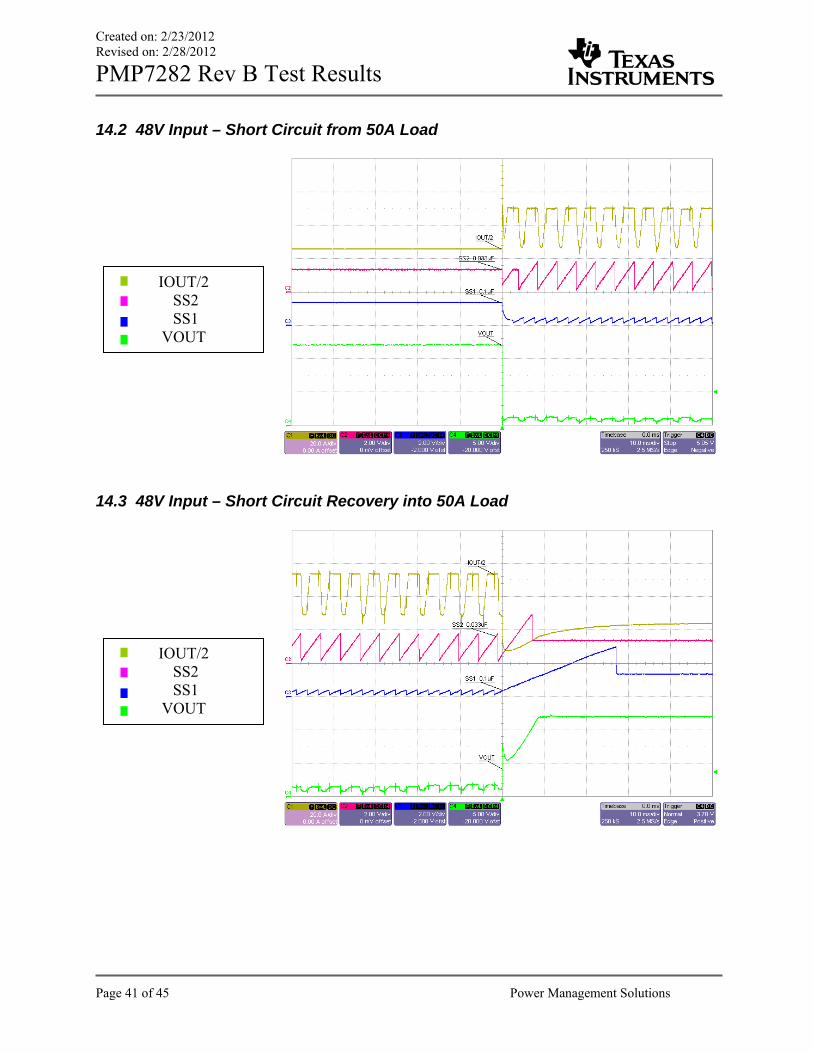
14 Short Circuit ............................................................................................................ 40 14.1 48V Input – Short Circuit from 50A Load .......................................................... 40 14.2 48V Input – Short Circuit from 50A Load .......................................................... 41 14.3 48V Input – Short Circuit Recovery into 50A Load............................................ 41 14.4 48V Input – Short Circuit Recovery into No Load ............................................. 42

15 Current Sharing ....................................................................................................... 43 15.1 48V Input – No Load......................................................................................... 44 15.2 48V Input – 25A Load ....................................................................................... 44 15.3 48V Input – 50A Load ....................................................................................... 45

16 LM5116 Bias Current .............................................................................................. 45

Created on: 2/23/2012 Revised on: 2/28/2012

PMP7282 Rev B Test Results

Page 4 of 45 Power Management Solutions

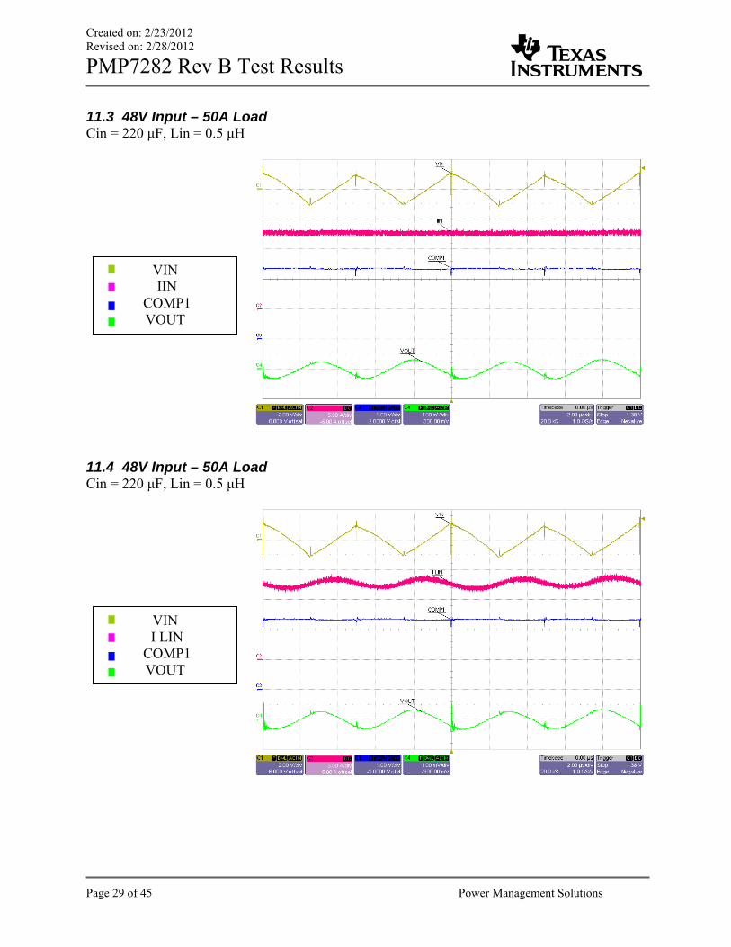
1 Circuit Description PMP7282 is a 2-phase buck converter capable of 600W output power. This design uses two LM5116 emulated current-mode synchronous buck controllers in a master/slave configuration. An LMC555 timer provides synchronization with 180 degrees between the two phases to mini-mize input and output ripple current. Current sharing is accomplished using an LMC7101 op amp, which forces the control voltage of the slave to follow that of the master. An LMV431 is used to control a pass regulator for the 5V op amp and timer supply. The LMV431 also provides the reference voltage for the op amp, which matches the internal reference of the LM5116 for proper tracking. Unless otherwise noted, test results are with Cin = 220 μF, Lin = 0.5 μH and Cout external = 2 x 270 μF. 2 Photo The circuit was built on PMP7282 Rev A printed circuit board. This is a four layer, 2 ounce cop-per board with overall dimensions of 2.30” x 3.05”, equivalent to two quarter-brick footprints. All components are mounted on the top side of the board.

Created on: 2/23/2012 Revised on: 2/28/2012

PMP7282 Rev B Test Results

Page 5 of 45 Power Management Solutions

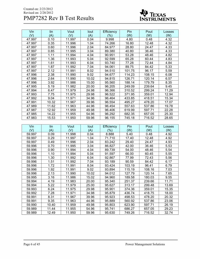
3 Efficiency The efficiency data is shown in the graph and tables below.

LM5116 2-Phase Buck Effiiency

85.000

90.000

95.000

100.000

0.00 10.00 20.00 30.00 40.00 50.00 60.00

Iout (A)

Eff

icie

ncy

(%

)

Vin = 35V

Vin = 48V

Vin = 60V

Vin (V)

Iin (A)

Vout (V)

Iout (A)

Efficiency (%)

Pin (W)

Pout (W)

Losses (W)

34.996 0.11 11.997 0.04 12.466 3.85 0.48 3.37 34.996 0.45 11.996 1.04 79.221 15.75 12.48 3.27 34.996 0.80 11.995 2.04 87.402 28.00 24.47 3.53 34.996 1.14 11.995 3.04 91.401 39.90 36.46 3.43 34.996 1.49 11.994 4.04 92.927 52.14 48.46 3.69 34.996 1.83 11.993 5.02 94.007 64.04 60.20 3.84 34.996 2.18 11.992 6.02 94.627 76.29 72.19 4.10 34.996 2.53 11.992 7.02 95.080 88.54 84.18 4.36 34.996 2.88 11.991 8.02 95.415 100.79 96.17 4.62 34.996 3.23 11.990 9.02 95.676 113.04 108.15 4.89 34.996 3.58 11.989 10.02 95.885 125.29 120.13 5.16 34.996 5.32 11.986 15.00 96.569 186.18 179.79 6.39 34.996 7.06 11.982 20.00 96.992 247.07 239.64 7.43 34.996 8.80 11.978 24.98 97.157 307.96 299.21 8.75 34.996 10.55 11.974 29.98 97.230 369.21 358.98 10.23 34.996 12.31 11.970 34.96 97.138 430.80 418.47 12.33 34.996 14.07 11.967 39.96 97.118 492.39 478.20 14.19 34.996 15.83 11.963 44.94 97.045 553.99 537.62 16.37 34.997 17.61 11.958 49.96 96.937 616.30 597.42 18.88 34.997 19.38 11.954 54.96 96.867 678.24 656.99 21.25 34.998 21.16 11.950 59.94 96.722 740.56 716.28 24.27

Created on: 2/23/2012 Revised on: 2/28/2012

PMP7282 Rev B Test Results

Page 6 of 45 Power Management Solutions

Vin (V)

Iin (A)

Vout (V)

Iout (A)

Efficiency (%)

Pin (W)

Pout (W)

Losses (W)

47.997 0.10 11.997 0.04 9.998 4.80 0.48 4.32 47.997 0.35 11.996 1.04 74.266 16.80 12.48 4.32 47.997 0.60 11.996 2.04 84.977 28.80 24.47 4.33 47.997 0.85 11.995 3.04 89.380 40.80 36.46 4.33 47.997 1.11 11.994 4.04 90.951 53.28 48.46 4.82 47.997 1.36 11.993 5.04 92.599 65.28 60.44 4.83 47.997 1.61 11.993 6.04 93.740 77.28 72.44 4.84 47.997 1.87 11.992 7.04 94.061 89.75 84.42 5.33 47.997 2.12 11.991 8.02 94.510 101.75 96.17 5.59 47.996 2.38 11.990 9.02 94.677 114.23 108.15 6.08 47.996 2.64 11.990 10.02 94.815 126.71 120.14 6.57 47.996 3.92 11.986 15.00 95.560 188.14 179.79 8.35 47.995 5.19 11.982 20.00 96.205 249.09 239.64 9.45 47.994 6.47 11.979 24.98 96.366 310.52 299.24 11.29 47.993 7.75 11.975 29.98 96.522 371.95 359.01 12.94 47.992 9.04 11.971 34.96 96.464 433.85 418.51 15.34 47.991 10.32 11.967 39.96 96.554 495.27 478.20 17.07 47.989 11.62 11.963 44.96 96.454 557.63 537.86 19.78 47.987 12.92 11.959 49.98 96.406 619.99 597.71 22.28 47.985 14.22 11.955 54.96 96.292 682.35 657.05 25.30 47.983 15.53 11.950 59.96 96.155 745.18 716.52 28.65

Vin (V)

Iin (A)

Vout (V)

Iout (A)

Efficiency (%)

Pin (W)

Pout (W)

Losses (W)

59.997 0.09 11.998 0.04 8.888 5.40 0.48 4.92 59.997 0.29 11.997 1.04 71.710 17.40 12.48 4.92 59.997 0.49 11.996 2.04 83.242 29.40 24.47 4.93 59.996 0.70 11.995 3.04 86.827 42.00 36.46 5.53 59.996 0.90 11.994 4.04 89.739 54.00 48.46 5.54 59.996 1.10 11.994 5.04 91.597 66.00 60.45 5.55 59.996 1.30 11.992 6.04 92.867 77.99 72.43 5.56 59.996 1.51 11.992 7.04 93.189 90.59 84.42 6.17 59.996 1.72 11.991 8.04 93.424 103.19 96.41 6.79 59.996 1.92 11.991 9.02 93.894 115.19 108.16 7.03 59.996 2.13 11.990 10.02 94.012 127.79 120.14 7.65 59.995 3.16 11.986 15.02 94.960 189.58 180.03 9.55 59.994 4.19 11.983 20.00 95.340 251.37 239.66 11.71 59.994 5.22 11.979 25.00 95.627 313.17 299.48 13.69 59.993 6.24 11.975 29.98 95.901 374.36 359.01 15.35 59.992 7.28 11.971 34.98 95.879 436.74 418.75 18.00 59.991 8.31 11.967 39.96 95.923 498.53 478.20 20.32 59.991 9.35 11.963 44.96 95.889 560.92 537.86 23.06 59.990 10.40 11.959 49.98 95.803 623.90 597.71 26.19 59.989 11.44 11.955 54.96 95.741 686.27 657.05 29.23 59.989 12.49 11.950 59.96 95.630 749.26 716.52 32.74

Created on: 2/23/2012 Revised on: 2/28/2012

PMP7282 Rev B Test Results

Page 7 of 45 Power Management Solutions

4 Thermal Test Summary Thermal tests were performed at 25°C ambient. Test conditions are 48V input with 50A load. The test setup and summary of the temperature measurements are shown in the picture and table below.

Airflow (LFM)

PC Board (°C)

Bottom LM5116

(°C)

Bottom MOSFETs

(°C)

Bottom Inductor Winding

(°C)

Top LM5116

(°C)

Top MOSFETs

(°C)

Top Inductor Winding

(°C) 1 hour soak time

0 171 139 161 157 157 176 168 20 minute soak time

200 126 91.3 113 110 106 129 120 20 minute soak time

400 105 81.4 98.1 90.5 89.1 105 98.6

Created on: 2/23/2012 Revised on: 2/28/2012

PMP7282 Rev B Test Results

Page 8 of 45 Power Management Solutions

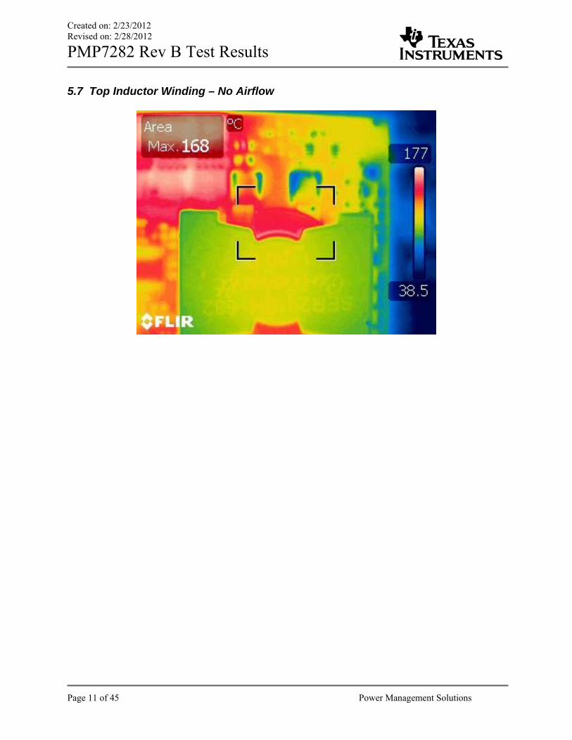
5 Thermal Images – No Airflow The thermal images show the top view of the board at 25°C ambient with no airflow. Test condi-tions are 48V input with 50A load. 5.1 PC Board – No Airflow

5.2 Bottom LM5116 – No Airflow

Created on: 2/23/2012 Revised on: 2/28/2012

PMP7282 Rev B Test Results

Page 9 of 45 Power Management Solutions

5.3 Bottom MOSFETs – No Airflow

5.4 Bottom Inductor Winding – No Airflow

Created on: 2/23/2012 Revised on: 2/28/2012

PMP7282 Rev B Test Results

Page 10 of 45 Power Management Solutions

5.5 Top LM5116 – No Airflow

5.6 Top MOSFETs – No Airflow

Created on: 2/23/2012 Revised on: 2/28/2012

PMP7282 Rev B Test Results

Page 11 of 45 Power Management Solutions

5.7 Top Inductor Winding – No Airflow

Created on: 2/23/2012 Revised on: 2/28/2012

PMP7282 Rev B Test Results

Page 12 of 45 Power Management Solutions

6 Thermal Images – 200 LFM The thermal images show the top view of the board at 25°C ambient with 200 linear feet per minute airflow. Test conditions are 48V input with 50A load. 6.1 PC Board – 200 LFM

6.2 Bottom LM5116 – 200 LFM

Created on: 2/23/2012 Revised on: 2/28/2012

PMP7282 Rev B Test Results

Page 13 of 45 Power Management Solutions

6.3 Bottom MOSFETs – 200 LFM

6.4 Bottom Inductor Winding – 200 LFM

Created on: 2/23/2012 Revised on: 2/28/2012

PMP7282 Rev B Test Results

Page 14 of 45 Power Management Solutions

6.5 Top LM5116 – 200 LFM

6.6 Top MOSFETs – 200 LFM

Created on: 2/23/2012 Revised on: 2/28/2012

PMP7282 Rev B Test Results

Page 15 of 45 Power Management Solutions

6.7 Top Inductor Winding – 200 LFM

Created on: 2/23/2012 Revised on: 2/28/2012

PMP7282 Rev B Test Results

Page 16 of 45 Power Management Solutions

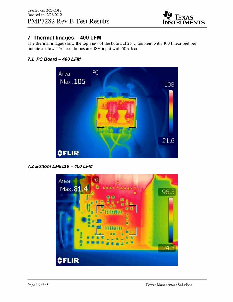
7 Thermal Images – 400 LFM The thermal images show the top view of the board at 25°C ambient with 400 linear feet per minute airflow. Test conditions are 48V input with 50A load. 7.1 PC Board – 400 LFM

7.2 Bottom LM5116 – 400 LFM

Created on: 2/23/2012 Revised on: 2/28/2012

PMP7282 Rev B Test Results

Page 17 of 45 Power Management Solutions

7.3 Bottom MOSFETs – 400 LFM

7.4 Bottom Inductor Winding – 400 LFM

Created on: 2/23/2012 Revised on: 2/28/2012

PMP7282 Rev B Test Results

Page 18 of 45 Power Management Solutions

7.5 Top LM5116 – 400 LFM

7.6 Top MOSFETs – 400 LFM

Created on: 2/23/2012 Revised on: 2/28/2012

PMP7282 Rev B Test Results

Page 19 of 45 Power Management Solutions

7.7 Top Inductor Winding – 400 LFM

Created on: 2/23/2012 Revised on: 2/28/2012

PMP7282 Rev B Test Results

Page 20 of 45 Power Management Solutions

8 Power Up and Power Down 8.1 Power Up at 48V Input – No Load

8.2 Power Up at 48V Input – 50A Load

VIN SS2 SS1

VOUT

VIN SS2 SS1

VOUT

Created on: 2/23/2012 Revised on: 2/28/2012

PMP7282 Rev B Test Results

Page 21 of 45 Power Management Solutions

8.3 Power Down at 48V Input – 50A Load

8.4 Power Down at 48V Input – No Load

VIN SS2 SS1

VOUT

VIN SS2 SS1

VOUT

Created on: 2/23/2012 Revised on: 2/28/2012

PMP7282 Rev B Test Results

Page 22 of 45 Power Management Solutions

9 Switching 9.1 35V Input – 50A Load

9.2 48V Input – 50A Load

SW1 LO1 SW2 LO2

SW1 LO1 SW2 LO2

Created on: 2/23/2012 Revised on: 2/28/2012

PMP7282 Rev B Test Results

Page 23 of 45 Power Management Solutions

9.3 60V Input – 50A Load

SW1 LO1 SW2 LO2

Created on: 2/23/2012 Revised on: 2/28/2012

PMP7282 Rev B Test Results

Page 24 of 45 Power Management Solutions

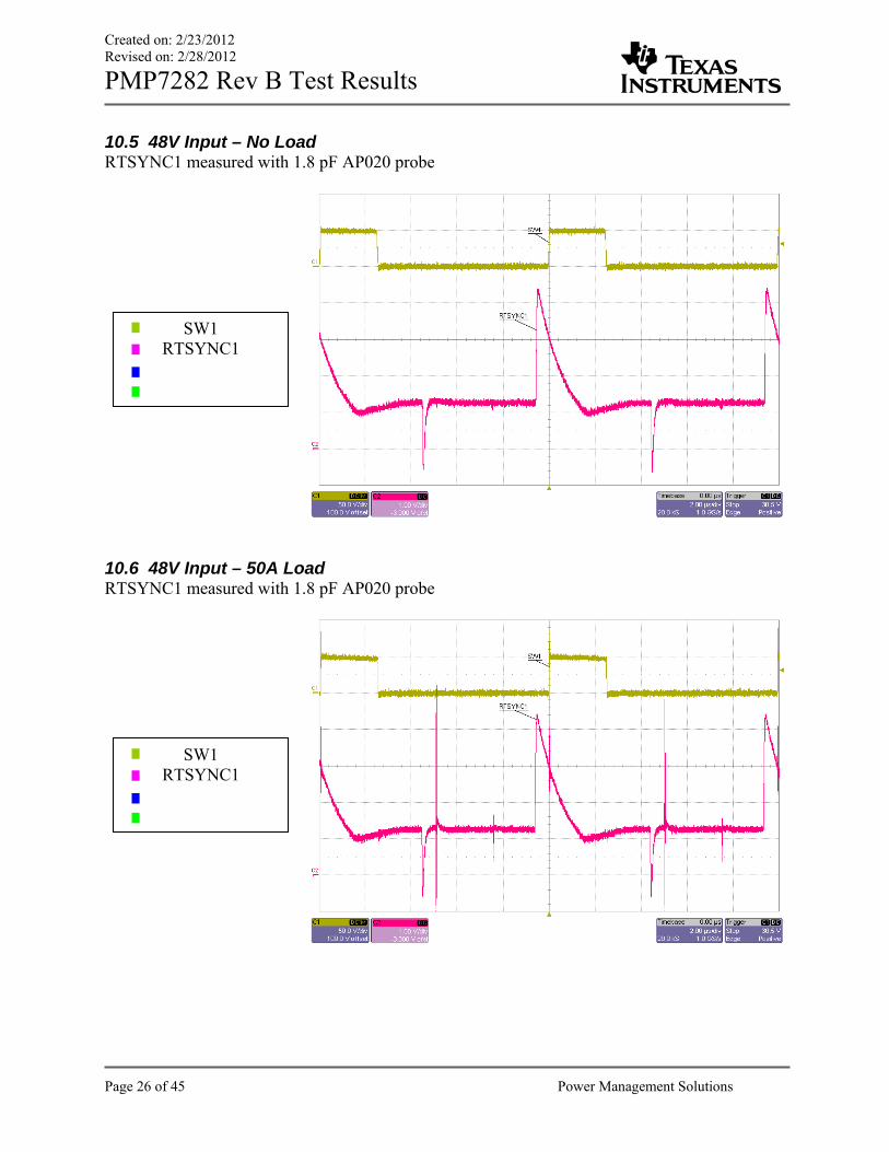
10 Synchronization 10.1 48V Input – No Load

10.2 48V Input – 50A Load

SW1 SYNC1

SW2 SYNC2

SW1 SYNC1

SW2 SYNC1

Created on: 2/23/2012 Revised on: 2/28/2012

PMP7282 Rev B Test Results

Page 25 of 45 Power Management Solutions

10.3 48V Input – No Load

10.4 48V Input – 50A Load

SW1 RTSYNC1

SW2 RTSYNC2

SW1 RTSYNC1

SW2 RTSYNC2

Created on: 2/23/2012 Revised on: 2/28/2012

PMP7282 Rev B Test Results

Page 26 of 45 Power Management Solutions

10.5 48V Input – No Load RTSYNC1 measured with 1.8 pF AP020 probe

10.6 48V Input – 50A Load RTSYNC1 measured with 1.8 pF AP020 probe

SW1 RTSYNC1

SW1 RTSYNC1

Created on: 2/23/2012 Revised on: 2/28/2012

PMP7282 Rev B Test Results

Page 27 of 45 Power Management Solutions

10.7 48V Input – No Load RTSYNC2 measured with 1.8 pF AP020 probe

10.8 48V Input – 50A Load RTSYNC2 measured with 1.8 pF AP020 probe

SW2 RTSYNC2

SW2 RTSYNC2

Created on: 2/23/2012 Revised on: 2/28/2012

PMP7282 Rev B Test Results

Page 28 of 45 Power Management Solutions

11 Ripple Voltage and Current 11.1 48V Input – 50A Load Cin = 220 μF + 0.5Ω damping resistor, Lin = 0 μH

11.2 48V Input – 50A Load Cin = 220 μF + 0.5Ω damping resistor, Lin = 0 μH

VIN I CIN

COMP1 VOUT

VIN IIN

COMP1 VOUT

Created on: 2/23/2012 Revised on: 2/28/2012

PMP7282 Rev B Test Results

Page 29 of 45 Power Management Solutions

11.3 48V Input – 50A Load Cin = 220 μF, Lin = 0.5 μH

11.4 48V Input – 50A Load Cin = 220 μF, Lin = 0.5 μH

VIN IIN

COMP1 VOUT

VIN I LIN

COMP1 VOUT

Created on: 2/23/2012 Revised on: 2/28/2012

PMP7282 Rev B Test Results

Page 30 of 45 Power Management Solutions

11.5 48V Input – 50A Load Cin = 220 μF, Lin = 0.5 μH

VIN I CIN

COMP1 VOUT

Created on: 2/23/2012 Revised on: 2/28/2012

PMP7282 Rev B Test Results

Page 31 of 45 Power Management Solutions

12 Transient Response with Rcomp = 7.5 kΩ (Rev A) Using Rcomp = 7.5 kΩ allows for higher bandwidth and faster transient response, but requires the use of external capacitors for stability. 12.1 48V Input – 25A Load Step Cin = 220 μF + 0.5Ω damping resistor, Lin = 0 μH, Cout external = 2 x 270 μF

12.2 48V Input – 25A Load Step Cin = 220 μF + 0.5Ω damping resistor, Lin = 0 μH, Cout external = 2 x 270 μF

VIN ILOAD/2 COMP1 VOUT

VIN ILOAD/2 COMP2 VOUT

Created on: 2/23/2012 Revised on: 2/28/2012

PMP7282 Rev B Test Results

Page 32 of 45 Power Management Solutions

12.3 48V Input – 25A Load Step Cin = 220 μF + 0.5Ω damping resistor, Lin = 0 μH, Cout external = 2 x 270 μF

12.4 48V Input – 25A Load Step Cin = 220 μF, Lin = 0.5 μH, Cout external = 2 x 270 μF

VIN ILOAD/2

REF2 VOUT

VIN ILOAD/2 COMP1 VOUT

Created on: 2/23/2012 Revised on: 2/28/2012

PMP7282 Rev B Test Results

Page 33 of 45 Power Management Solutions

12.5 35V Input – 25A Load Step Cin = 220 μF, Lin = 0.5 μH, Cout external = 2 x 270 μF

12.6 60V Input – 25A Load Step Cin = 220 μF, Lin = 0.5 μH, Cout external = 2 x 270 μF

VIN ILOAD/2 COMP1 VOUT

VIN ILOAD/2 COMP1 VOUT

Created on: 2/23/2012 Revised on: 2/28/2012

PMP7282 Rev B Test Results

Page 34 of 45 Power Management Solutions

12.7 48V Input – 25A Load Step Cin = 220 μF, Lin = 0.5 μH, Cout external = 1 x 270 μF

12.8 48V Input – 1A Load Cin = 220 μF, Lin = 0.5 μH, Cout external = 0 μF resulting in feedback oscillation

VIN ILOAD/2 COMP1 VOUT

VIN ILOAD/2 COMP1 VOUT

Created on: 2/23/2012 Revised on: 2/28/2012

PMP7282 Rev B Test Results

Page 35 of 45 Power Management Solutions

12.9 48V Input – 1A Load Cin = 220 μF, Lin = 0.5 μH, Cout external = 0 μF resulting in feedback oscillation

VIN ILOAD/2 COMP2 VOUT

Created on: 2/23/2012 Revised on: 2/28/2012

PMP7282 Rev B Test Results

Page 36 of 45 Power Management Solutions

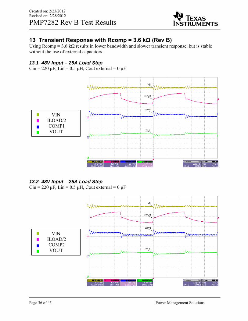
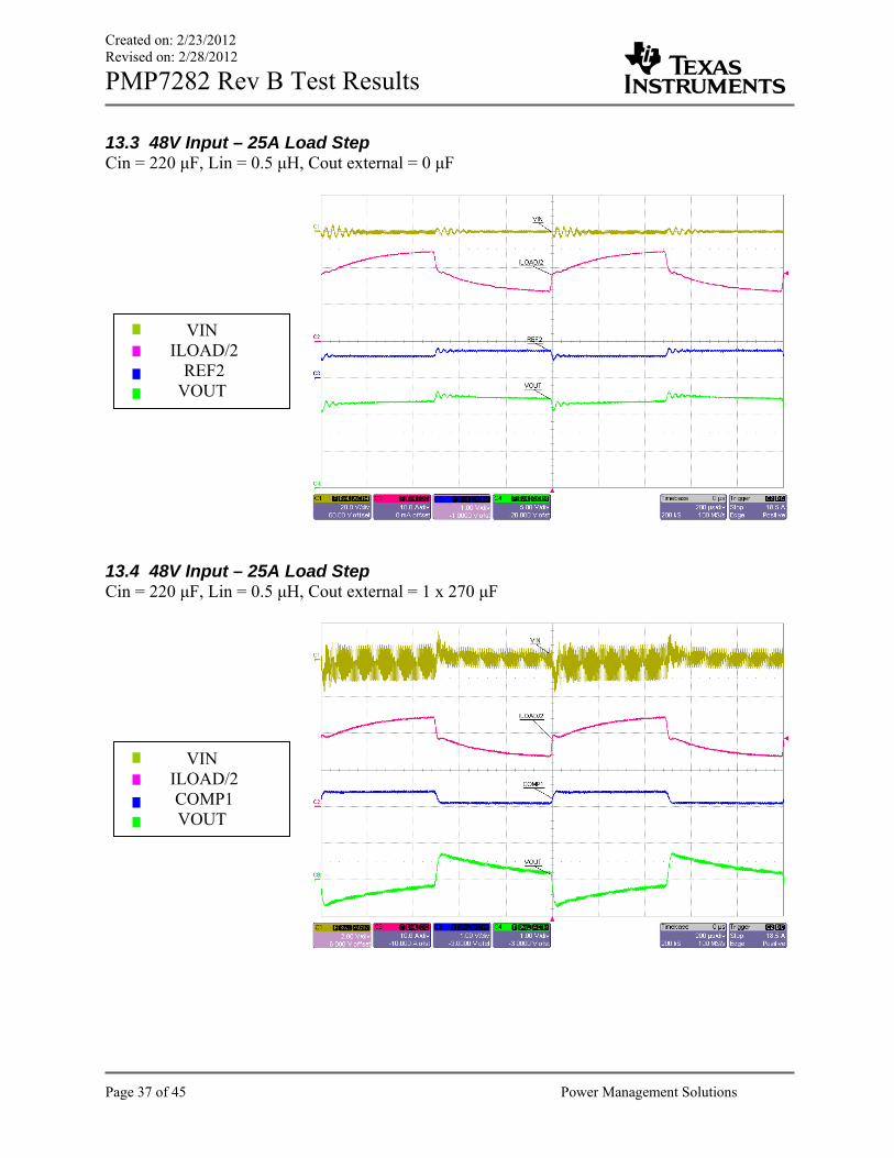
13 Transient Response with Rcomp = 3.6 kΩ (Rev B) Using Rcomp = 3.6 kΩ results in lower bandwidth and slower transient response, but is stable without the use of external capacitors. 13.1 48V Input – 25A Load Step Cin = 220 μF, Lin = 0.5 μH, Cout external = 0 μF

13.2 48V Input – 25A Load Step Cin = 220 μF, Lin = 0.5 μH, Cout external = 0 μF

VIN ILOAD/2 COMP1 VOUT

VIN ILOAD/2 COMP2 VOUT

Created on: 2/23/2012 Revised on: 2/28/2012

PMP7282 Rev B Test Results

Page 37 of 45 Power Management Solutions

13.3 48V Input – 25A Load Step Cin = 220 μF, Lin = 0.5 μH, Cout external = 0 μF

13.4 48V Input – 25A Load Step Cin = 220 μF, Lin = 0.5 μH, Cout external = 1 x 270 μF

VIN ILOAD/2

REF2 VOUT

VIN ILOAD/2 COMP1 VOUT

Created on: 2/23/2012 Revised on: 2/28/2012

PMP7282 Rev B Test Results

Page 38 of 45 Power Management Solutions

13.5 48V Input – 25A Load Step Cin = 220 μF, Lin = 0.5 μH, Cout external = 2 x 270 μF

13.6 35V Input – 25A Load Step Cin = 220 μF, Lin = 0.5 μH, Cout external = 2 x 270 μF

VIN ILOAD/2 COMP1 VOUT

VIN ILOAD/2 COMP1 VOUT

Created on: 2/23/2012 Revised on: 2/28/2012

PMP7282 Rev B Test Results

Page 39 of 45 Power Management Solutions

13.7 60V Input – 25A Load Step Cin = 220 μF, Lin = 0.5 μH, Cout external = 2 x 270 μF

VIN ILOAD/2 COMP1 VOUT

Created on: 2/23/2012 Revised on: 2/28/2012

PMP7282 Rev B Test Results

Page 40 of 45 Power Management Solutions

14 Short Circuit Short circuit current - average value as measured through shunts

Vin (V)

Iin (A)

Vout (V)

Iout (A)

Pin (W)

Pout (W)

Pdis (W)

35 3.1 0.75 82 108.5 61.5 47.0 48 2.5 0.75 82 120.0 61.5 58.5 60 1.8 0.75 82 108.0 61.5 46.5

14.1 48V Input – Short Circuit from 50A Load

IIN SS2 SS1

VOUT

Created on: 2/23/2012 Revised on: 2/28/2012

PMP7282 Rev B Test Results

Page 41 of 45 Power Management Solutions

14.2 48V Input – Short Circuit from 50A Load

14.3 48V Input – Short Circuit Recovery into 50A Load

IOUT/2 SS2 SS1

VOUT

IOUT/2 SS2 SS1

VOUT

Created on: 2/23/2012 Revised on: 2/28/2012

PMP7282 Rev B Test Results

Page 42 of 45 Power Management Solutions

14.4 48V Input – Short Circuit Recovery into No Load

IOUT/2 SS2 SS1

VOUT

Created on: 2/23/2012 Revised on: 2/28/2012

PMP7282 Rev B Test Results

Page 43 of 45 Power Management Solutions

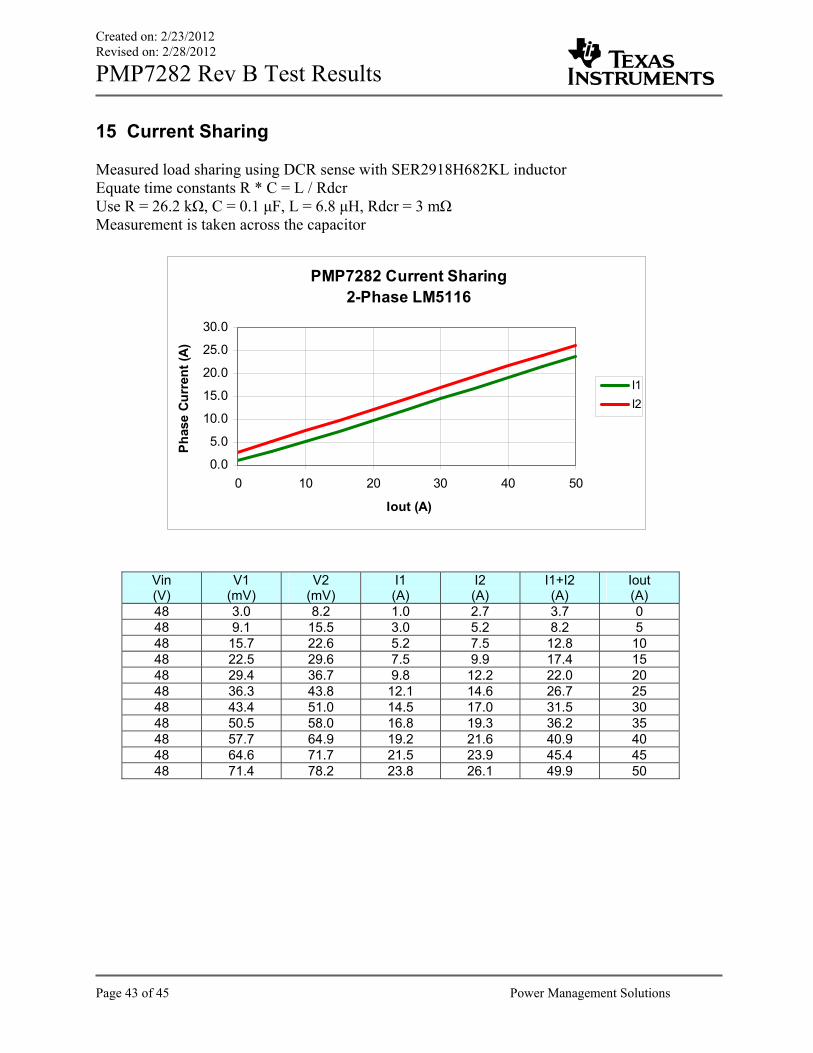
15 Current Sharing Measured load sharing using DCR sense with SER2918H682KL inductor Equate time constants R * C = L / Rdcr Use R = 26.2 kΩ, C = 0.1 μF, L = 6.8 μH, Rdcr = 3 mΩ Measurement is taken across the capacitor

PMP7282 Current Sharing2-Phase LM5116

0.0

5.0

10.0

15.0

20.0

25.0

30.0

0 10 20 30 40 50

Iout (A)

Ph

ase

Cu

rren

t (A

)

I1

I2

Vin (V)

V1 (mV)

V2 (mV)

I1 (A)

I2 (A)

I1+I2 (A)

Iout (A)

48 3.0 8.2 1.0 2.7 3.7 0 48 9.1 15.5 3.0 5.2 8.2 5 48 15.7 22.6 5.2 7.5 12.8 10 48 22.5 29.6 7.5 9.9 17.4 15 48 29.4 36.7 9.8 12.2 22.0 20 48 36.3 43.8 12.1 14.6 26.7 25 48 43.4 51.0 14.5 17.0 31.5 30 48 50.5 58.0 16.8 19.3 36.2 35 48 57.7 64.9 19.2 21.6 40.9 40 48 64.6 71.7 21.5 23.9 45.4 45 48 71.4 78.2 23.8 26.1 49.9 50

Created on: 2/23/2012 Revised on: 2/28/2012

PMP7282 Rev B Test Results

Page 44 of 45 Power Management Solutions

15.1 48V Input – No Load

15.2 48V Input – 25A Load

VDCR1

VDCR2

VDCR1

VDCR2

Created on: 2/23/2012 Revised on: 2/28/2012

PMP7282 Rev B Test Results

Page 45 of 45 Power Management Solutions

15.3 48V Input – 50A Load

VDCR1

VDCR2

16 LM5116 Bias Current LM5116 bias current to VCCX - measured across 1 ohm resistor from VOUT

Vin (V)

I U1 (mA)

I U5 (mA)

Iout (A)

35 32.8 28.9 0 35 33.2 29.1 25 35 33.3 29.2 50

48 33.1 29.2 0 48 33.3 29.2 25 48 33.4 29.3 50

60 33.3 29.4 0 60 33.6 29.6 25 60 33.7 29.5 50

IMPORTANT NOTICE

Texas Instruments Incorporated and its subsidiaries (TI) reserve the right to make corrections, enhancements, improvements and otherchanges to its semiconductor products and services per JESD46, latest issue, and to discontinue any product or service per JESD48, latestissue. Buyers should obtain the latest relevant information before placing orders and should verify that such information is current andcomplete. All semiconductor products (also referred to herein as “components”) are sold subject to TI’s terms and conditions of salesupplied at the time of order acknowledgment.

TI warrants performance of its components to the specifications applicable at the time of sale, in accordance with the warranty in TI’s termsand conditions of sale of semiconductor products. Testing and other quality control techniques are used to the extent TI deems necessaryto support this warranty. Except where mandated by applicable law, testing of all parameters of each component is not necessarilyperformed.

TI assumes no liability for applications assistance or the design of Buyers’ products. Buyers are responsible for their products andapplications using TI components. To minimize the risks associated with Buyers’ products and applications, Buyers should provideadequate design and operating safeguards.

TI does not warrant or represent that any license, either express or implied, is granted under any patent right, copyright, mask work right, orother intellectual property right relating to any combination, machine, or process in which TI components or services are used. Informationpublished by TI regarding third-party products or services does not constitute a license to use such products or services or a warranty orendorsement thereof. Use of such information may require a license from a third party under the patents or other intellectual property of thethird party, or a license from TI under the patents or other intellectual property of TI.

Reproduction of significant portions of TI information in TI data books or data sheets is permissible only if reproduction is without alterationand is accompanied by all associated warranties, conditions, limitations, and notices. TI is not responsible or liable for such altereddocumentation. Information of third parties may be subject to additional restrictions.

Resale of TI components or services with statements different from or beyond the parameters stated by TI for that component or servicevoids all express and any implied warranties for the associated TI component or service and is an unfair and deceptive business practice.TI is not responsible or liable for any such statements.

Buyer acknowledges and agrees that it is solely responsible for compliance with all legal, regulatory and safety-related requirementsconcerning its products, and any use of TI components in its applications, notwithstanding any applications-related information or supportthat may be provided by TI. Buyer represents and agrees that it has all the necessary expertise to create and implement safeguards whichanticipate dangerous consequences of failures, monitor failures and their consequences, lessen the likelihood of failures that might causeharm and take appropriate remedial actions. Buyer will fully indemnify TI and its representatives against any damages arising out of the useof any TI components in safety-critical applications.

In some cases, TI components may be promoted specifically to facilitate safety-related applications. With such components, TI’s goal is tohelp enable customers to design and create their own end-product solutions that meet applicable functional safety standards andrequirements. Nonetheless, such components are subject to these terms.

No TI components are authorized for use in FDA Class III (or similar life-critical medical equipment) unless authorized officers of the partieshave executed a special agreement specifically governing such use.

Only those TI components which TI has specifically designated as military grade or “enhanced plastic” are designed and intended for use inmilitary/aerospace applications or environments. Buyer acknowledges and agrees that any military or aerospace use of TI componentswhich have not been so designated is solely at the Buyer's risk, and that Buyer is solely responsible for compliance with all legal andregulatory requirements in connection with such use.

TI has specifically designated certain components which meet ISO/TS16949 requirements, mainly for automotive use. Components whichhave not been so designated are neither designed nor intended for automotive use; and TI will not be responsible for any failure of suchcomponents to meet such requirements.

Products Applications

Audio www.ti.com/audio Automotive and Transportation www.ti.com/automotive

Amplifiers amplifier.ti.com Communications and Telecom www.ti.com/communications

Data Converters dataconverter.ti.com Computers and Peripherals www.ti.com/computers

DLP® Products www.dlp.com Consumer Electronics www.ti.com/consumer-apps

DSP dsp.ti.com Energy and Lighting www.ti.com/energy

Clocks and Timers www.ti.com/clocks Industrial www.ti.com/industrial

Interface interface.ti.com Medical www.ti.com/medical

Logic logic.ti.com Security www.ti.com/security

Power Mgmt power.ti.com Space, Avionics and Defense www.ti.com/space-avionics-defense

Microcontrollers microcontroller.ti.com Video and Imaging www.ti.com/video

RFID www.ti-rfid.com

OMAP Applications Processors www.ti.com/omap TI E2E Community e2e.ti.com

Wireless Connectivity www.ti.com/wirelessconnectivity

Mailing Address: Texas Instruments, Post Office Box 655303, Dallas, Texas 75265Copyright © 2012, Texas Instruments Incorporated


Recommended