Product Folder Sample & Buy Technical Documents Tools & Software Support & Community LM556 SNAS549A – MARCH 2000 – REVISED OCTOBER 2015 LM556 Dual Timer 1 Features 3 Description The LM556 dual-timing circuit is a highly-stable 1• Direct Replacement for SE556/NE556 controller capable of producing accurate time delays • Timing From Microseconds Through Hours or oscillation. The LM556 device is a dual-timing • Operates in Both Astable and Monostable Modes version of the LM555 device. Timing is provided by an external resistor and capacitor for each timing • Replaces Two 555 Timers function. The two timers operate independently of • Adjustable Duty Cycle each other, sharing only V CC and ground. The circuits • Output Can Source or Sink 200 mA may be triggered and reset on falling waveforms. The output structures may sink or source 200 mA. • Output and Supply TTL-Compatible • Temperature Stability Better Than 0.005% per °C Device Information (1) • Normally On and Normally Off Output PART NUMBER PACKAGE BODY SIZE (NOM) SOIC (14) 3.91 mm × 8.65 mm 2 Applications LM556 PDIP (14) 6.35 mm × 19.177 mm • Precision Timing (1) For all available packages, see the orderable addendum at • Pulse Generation the end of the data sheet. • Sequential Timing • Time Delay Generation • Pulse Width Modulation • Pulse Position Modulation • Linear Ramp Generator Schematic Diagram 1 An IMPORTANT NOTICE at the end of this data sheet addresses availability, warranty, changes, use in safety-critical applications, intellectual property matters and other important disclaimers. PRODUCTION DATA.
Transcript
Product
Folder
Sample &Buy
Technical
Documents
Tools &
Software
Support &Community
LM556SNAS549A –MARCH 2000–REVISED OCTOBER 2015
LM556 Dual Timer1 Features 3 Description
The LM556 dual-timing circuit is a highly-stable1• Direct Replacement for SE556/NE556
controller capable of producing accurate time delays• Timing From Microseconds Through Hours or oscillation. The LM556 device is a dual-timing• Operates in Both Astable and Monostable Modes version of the LM555 device. Timing is provided by
an external resistor and capacitor for each timing• Replaces Two 555 Timersfunction. The two timers operate independently of• Adjustable Duty Cycle each other, sharing only VCC and ground. The circuits
• Output Can Source or Sink 200 mA may be triggered and reset on falling waveforms. Theoutput structures may sink or source 200 mA.• Output and Supply TTL-Compatible
• Temperature Stability Better Than 0.005% per °CDevice Information(1)
• Normally On and Normally Off OutputPART NUMBER PACKAGE BODY SIZE (NOM)
SOIC (14) 3.91 mm × 8.65 mm2 Applications LM556PDIP (14) 6.35 mm × 19.177 mm
• Precision Timing(1) For all available packages, see the orderable addendum at• Pulse Generation the end of the data sheet.
• Sequential Timing• Time Delay Generation• Pulse Width Modulation• Pulse Position Modulation• Linear Ramp Generator
Schematic Diagram
1
An IMPORTANT NOTICE at the end of this data sheet addresses availability, warranty, changes, use in safety-critical applications,intellectual property matters and other important disclaimers. PRODUCTION DATA.
LM556SNAS549A –MARCH 2000–REVISED OCTOBER 2015 www.ti.com
Table of Contents7.4 Device Functional Modes.......................................... 81 Features .................................................................. 1
4 Revision HistoryNOTE: Page numbers for previous revisions may differ from page numbers in the current version.
Changes from Original (March 2000) to Revision A Page
• Added ESD Ratings table, Feature Description section, Device Functional Modes, Application and Implementationsection, Power Supply Recommendations section, Layout section, Device and Documentation Support section, andMechanical, Packaging, and Orderable Information section. ................................................................................................ 1
• Deleted the VCC = 5 V and ISINK = 8 mA test condition row for the Output voltage drop parameter in the ElectricalCharacteristics table ............................................................................................................................................................... 5
LM556www.ti.com SNAS549A –MARCH 2000–REVISED OCTOBER 2015
5 Pin Configuration and Functions
D or NFF Package14-Pin SOIC or PDIP
Top View
Pin FunctionsPIN
I/O DESCRIPTIONNAME NO.CONTROL Controls the threshold and trigger levels. It determines the pulse width of the outputVOLTAGE 3 I waveform. An external voltage applied to this pin can also be used to modulate the output(Timer 0) waveform.CONTROL Controls the threshold and trigger levels. It determines the pulse width of the outputVOLTAGE 11 I waveform. An external voltage applied to this pin can also be used to modulate the output(Timer 1) waveform.DISCHARGE Open collector output which discharges a capacitor between intervals (in phase with output).1 I(Timer 0) It toggles the output from high to low when voltage reaches 2/3 of supply voltage.DISCHARGE Open collector output which discharges a capacitor between intervals (in phase with output).13 I(Timer 1) It toggles the output from high to low when voltage reaches 2/3 of supply voltage.GND 7 O Ground reference voltageOUTPUT 5 O Output driven waveform(Timer 0)OUTPUT 9 O Output driven waveform(Timer 1)RESET Negative pulse applied to this pin to disable or reset the timer. When not used for reset4 I(Timer 0) purposes, it should be connected to Vcc to avoid false triggering.RESET Negative pulse applied to this pin to disable or reset the timer. When not used for reset10 I(Timer 1) purposes, it should be connected to Vcc to avoid false triggering.THRESHOLD Compares the voltage applied to the terminal with a reference voltage of 2/3 VCC. The2 I(Timer 0) amplitude of voltage applied to this terminal is responsible for the set state of the flip-flop.TRIGGER Responsible for transition of the flip-flop from set to reset. The output of the timer depends6 I(Timer 0) on the amplitude of the external trigger pulse applied to this pin.THRESHOLD Compares the voltage applied to the terminal with a reference voltage of 2/3 VCC. The12 I(Timer 1) amplitude of voltage applied to this terminal is responsible for the set state of the flip-flop.TRIGGER Responsible for transition of the flip-flop from set to reset. The output of the timer depends8 I(Timer 1) on the amplitude of the external trigger pulse applied to this pin.VCC 14 I Supply voltage with respect to GND
(1) Stresses beyond those listed under Absolute Maximum Ratings may cause permanent damage to the device. These are stress ratingsonly, which do not imply functional operation of the device at these or any other conditions beyond those indicated under RecommendedOperating Conditions. Exposure to absolute-maximum-rated conditions for extended periods may affect device reliability.
(2) If Military/Aerospace specified devices are required, please contact the National Semiconductor Sales Office/ Distributors for availabilityand specifications.
(3) For operating at elevated temperatures the device must be derated based on a 150°C maximum junction temperature and a thermalresistance of 77°C/W (Plastic Dip), and 110°C/W (SO-14 Narrow).
6.2 ESD RatingsVALUE UNIT
V(ESD) Electrostatic discharge Human body model (HBM), per ANSI/ESDA/JEDEC JS-001 (1) ±500 V
(1) JEDEC document JEP155 states that 500-V HBM allows safe manufacturing with a standard ESD control process.
6.3 Recommended Operating Conditionsover operating free-air temperature range (unless otherwise noted)
MIN MAX UNITVCC Supply voltage 4.5 16 VTA Operating temperature 0 70 °C
LM556www.ti.com SNAS549A –MARCH 2000–REVISED OCTOBER 2015
6.5 Electrical CharacteristicsTA = 25°C, VCC = 5 V to 15 V, unless otherwise specified
PARAMETER TEST CONDITIONS MIN TYP MAX UNIT
Supply voltage 4.5 16 V
VCC = 5 V, RL = ¥ 3 6Supply current (each timer section) mA
VCC = 15 V, RL = ¥ (low state) (1) 10 14
Initial accuracy 0.75%
Drift with temperature 50 ppm/°CTiming error, RA = 1 k to 100 kΩ,monostable C = 0.1 μF (2)
Accuracy over temperature 1.5%
Drift with supply 0.1%/V
Initial accuracy 2.25%
Drift with temperature 150Timing error, RA, RB = 1 k to 100 kΩ, ppm/°Castable C = 0.1 μF (2)Accuracy over temperature 3%
Drift with supply 0.30 %/V
VCC = 15 V 4.5 5 5.5Trigger voltage V
VCC = 5 V 1.25 1.67 2
Trigger current 0.2 1 µA
Reset voltage 0.4 0.5 1 V
Reset current 0.1 0.6 mA
VTH = V-control (3) 0.03 0.1 µAThreshold current
VTH = 11.2 V 250 nA
VCC = 15 V 9 10 11Control voltage level and threshold voltage V
VCC = 5 V 2.6 3.33 4
Pin 1, 13 leakage output high 1 100 nA
VCC = 15 V, I = 15 mA 180 300Pin 1, 13 sat output low (4) mV
VCC = 4.5 V, I = 4.5 mA 80 200
ISINK = 10 mA 0.1 0.25
ISINK = 50 mA 0.4 0.75VCC = 15 V
Output voltage drop (low) ISINK = 100 mA 2 2.75 V
ISINK = 200 mA 2.5
VCC = 5 V, ISINK = 5 mA 0.25 0.35
ISOURCE = 200 mA, VCC = 15 V 12.5
Output voltage drop (high) ISOURCE = 100 mA, VCC = 15 V 12.75 13.3 V
VCC = 5 V 2.75 3.3
Rise time of output 100 ns
Fall time of output 100 ns
Initial timing accuracy 0.1% 2%ppm/°CMatching Timing drift with temperature See (5) ±10characteristics
Drift with supply voltage 0.2 0.5 %/V
(1) Supply current when output high typically 1 mA less at VCC = 5 V.(2) Tested at VCC = 5 V and VCC = 15 V.(3) This will determine the maximum value of RA + RB for 15-V operation. The maximum total (RA + RB) is 20 MΩ.(4) No protection against excessive pin 1, 13 current is necessary providing the package dissipation rating will not be exceeded.(5) Matching characteristics refer to the difference between performance characteristics of each timer section.
LM556SNAS549A –MARCH 2000–REVISED OCTOBER 2015 www.ti.com
7 Detailed Description
7.1 OverviewThe LM556 dual-timing circuit is a highly stable device for generating accurate time delays or oscillations. Thetwo timers operate independently from one another, only sharing VCC and ground. For each individual timer,additional terminals are provided for triggering or resetting. In the monostable mode of operation, the time isprecisely controlled by one external resistor and capacitor. For astable mode operation as an oscillator, the freerunning frequency and duty cycle are accurately controlled with two external resistors and one capacitor. Thecircuit may be triggered and reset on falling waveforms and the output circuit can source or sink up to 200 mA.
7.2 Functional Block Diagram
7.3 Feature Description
7.3.1 Operating CharacteristicsThe LM556 is specified for operation from 4.5 V to 16 V. Many of the specifications apply from 0⁰C to 70⁰C.Parameters that can exhibit significant variance with regard to operating voltage or temperature are presentedElectrical Characteristics section and in and Typical Characteristics.
7.3.2 Timing from Microseconds Through HoursThe LM556 has the ability to have timing parameters from the microseconds range to hours. The time delay ofthe system can be determined by the time constant of the R and C values used for either the monostable orastable configuration. A nomograph is available for easy determination of R and C values for various time delays.
7.4 Device Functional ModesThe LM556 can operate in both astable and monostable mode depending on the application requirements.
7.4.1 Monostable ModeThe LM556 timer acts as a one-shot pulse generator. The pulse begins when the LM556 timer receives a signalat the trigger input that falls below 1/3 of the voltage supply. The width of the output pulse is determined by thetime constant of an RC network. The output pulse ends when the voltage on the capacitor equals 2/3 of thesupply voltage. The output pulse width can be extended or shortened depending on the application by adjustingthe R and C values. More details are given in the LM555 datasheet (SNAS548).
LM556www.ti.com SNAS549A –MARCH 2000–REVISED OCTOBER 2015
Device Functional Modes (continued)
Figure 11. Monostable
7.4.2 Astable (Free-Running) ModeThe LM556 timer can operate as an oscillator and puts out a continuous stream of rectangular pulses having aspecified frequency. The frequency of the pulse stream depends on the values of RA, RB, and C. Again, moredetails are given in the LM555 datasheet (SNAS548).
LM556SNAS549A –MARCH 2000–REVISED OCTOBER 2015 www.ti.com
8 Application and Implementation
NOTEInformation in the following applications sections is not part of the TI componentspecification, and TI does not warrant its accuracy or completeness. TI’s customers areresponsible for determining suitability of components for their purposes. Customers shouldvalidate and test their design implementation to confirm system functionality.
8.1 Application InformationThe LM556 timer can be used in various configurations. A typical application for the LM556 timer in astablemode is to drive an audio device (such as a beeper) to provide a pulsed sound. This simple application can bemodified to fit any application requirement.
8.2 Typical Application
Figure 13. Typical Application
8.2.1 Design RequirementsThe main design requirements for this application require setting one of the timers (Timer A in this case) to thesame resonant frequency as the piezo transducer which can be set by choosing R1A, R2A, and CA withEquation 1:
(1)
The other design choice is to decide how often and long to produce the bleeping sound. This can be set bychoosing R1B and R2B of Timer B (acts as the reset button for Timer A) with Equation 2:
(2)
Other useful design equations like Equation 3 and Equation 4 are given below where th represents the time ittakes to charge the capacitor of each individual timer and tl represents the time it takes to discharge thecapacitor.
LM556www.ti.com SNAS549A –MARCH 2000–REVISED OCTOBER 2015
Typical Application (continued)
where• th represents the time it takes to charge the capacitor of each individual timer (3)
where• tl represents the time it takes to discharge the capacitor. (4)
8.2.2 Detailed Design ProcedureGiven that the resonant frequency of the piezo transducer is about 3 kHz, by choosing R1, C and usingEquation 1, R2 can be determined to be 23.5 kΩ.
In order to have the sound be audible for half the period, the duty cycle for the triggering timer should be 50%.However, this is difficult to achieve because the recommended minimum value for R1 is 1 kΩ. Therefore, a dutycycle of 49% was chosen for this application. By choosing R1 to be 1 kΩ and using Equation 2, R2 is found to be24.5 kΩ.
8.2.3 Application Curve
Figure 14. Capacitor Voltage and Output Waveforms in Astable Mode
LM556SNAS549A –MARCH 2000–REVISED OCTOBER 2015 www.ti.com
9 Power Supply RecommendationsThe LM556 requires a voltage supply within 4.5 V to 16 V. Adequate power supply bypassing is necessary toprotect associated circuitry. The minimum recommended capacitor value is 0.1 µF in parallel with a 1-µFelectrolytic capacitor. Place the bypass capacitors as close as possible to the LM556 and minimize the tracelength
CAUTIONSupply voltages larger than 18 V can permanently damage the device; see theAbsolute Maximum Ratings table.
10 Layout
10.1 Layout GuidelinesStandard PCB rules apply to routing the LM556. The parallel combination of a 0.1-µF capacitor and a 1-µFelectrolytic capacitor should be as close as possible to the LM556. The capacitor used for the time delay shouldalso be placed as close as possible to the discharge pin. A ground plane on the bottom layer can be used toprovide better noise immunity and signal integrity.
LM556www.ti.com SNAS549A –MARCH 2000–REVISED OCTOBER 2015
11 Device and Documentation Support
11.1 Documentation Support
11.1.1 Related DocumentationFor related documentation, see the following:
LM555 Timer, SNAS548
11.2 Community ResourcesThe following links connect to TI community resources. Linked contents are provided "AS IS" by the respectivecontributors. They do not constitute TI specifications and do not necessarily reflect TI's views; see TI's Terms ofUse.
TI E2E™ Online Community TI's Engineer-to-Engineer (E2E) Community. Created to foster collaborationamong engineers. At e2e.ti.com, you can ask questions, share knowledge, explore ideas and helpsolve problems with fellow engineers.
Design Support TI's Design Support Quickly find helpful E2E forums along with design support tools andcontact information for technical support.
11.3 TrademarksE2E is a trademark of Texas Instruments.All other trademarks are the property of their respective owners.
11.4 Electrostatic Discharge CautionThese devices have limited built-in ESD protection. The leads should be shorted together or the device placed in conductive foamduring storage or handling to prevent electrostatic damage to the MOS gates.
11.5 GlossarySLYZ022 — TI Glossary.
This glossary lists and explains terms, acronyms, and definitions.
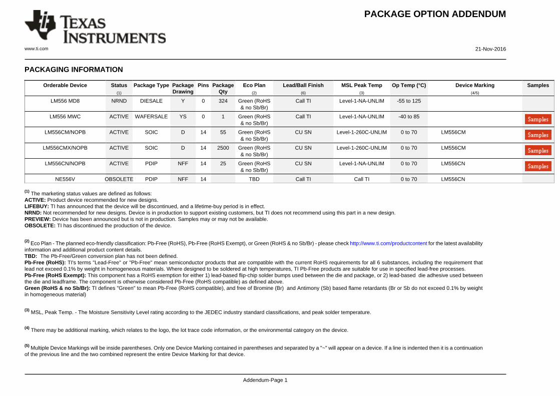
12 Mechanical, Packaging, and Orderable InformationThe following pages include mechanical, packaging, and orderable information. This information is the mostcurrent data available for the designated devices. This data is subject to change without notice and revision ofthis document. For browser-based versions of this data sheet, refer to the left-hand navigation.
LM556 MD8 NRND DIESALE Y 0 324 Green (RoHS& no Sb/Br)
Call TI Level-1-NA-UNLIM -55 to 125
LM556 MWC ACTIVE WAFERSALE YS 0 1 Green (RoHS& no Sb/Br)
Call TI Level-1-NA-UNLIM -40 to 85
LM556CM/NOPB ACTIVE SOIC D 14 55 Green (RoHS& no Sb/Br)
CU SN Level-1-260C-UNLIM 0 to 70 LM556CM
LM556CMX/NOPB ACTIVE SOIC D 14 2500 Green (RoHS& no Sb/Br)
CU SN Level-1-260C-UNLIM 0 to 70 LM556CM
LM556CN/NOPB ACTIVE PDIP NFF 14 25 Green (RoHS& no Sb/Br)
CU SN Level-1-NA-UNLIM 0 to 70 LM556CN
NE556V OBSOLETE PDIP NFF 14 TBD Call TI Call TI 0 to 70 LM556CN (1) The marketing status values are defined as follows:ACTIVE: Product device recommended for new designs.LIFEBUY: TI has announced that the device will be discontinued, and a lifetime-buy period is in effect.NRND: Not recommended for new designs. Device is in production to support existing customers, but TI does not recommend using this part in a new design.PREVIEW: Device has been announced but is not in production. Samples may or may not be available.OBSOLETE: TI has discontinued the production of the device.
(2) Eco Plan - The planned eco-friendly classification: Pb-Free (RoHS), Pb-Free (RoHS Exempt), or Green (RoHS & no Sb/Br) - please check http://www.ti.com/productcontent for the latest availabilityinformation and additional product content details.TBD: The Pb-Free/Green conversion plan has not been defined.Pb-Free (RoHS): TI's terms "Lead-Free" or "Pb-Free" mean semiconductor products that are compatible with the current RoHS requirements for all 6 substances, including the requirement thatlead not exceed 0.1% by weight in homogeneous materials. Where designed to be soldered at high temperatures, TI Pb-Free products are suitable for use in specified lead-free processes.Pb-Free (RoHS Exempt): This component has a RoHS exemption for either 1) lead-based flip-chip solder bumps used between the die and package, or 2) lead-based die adhesive used betweenthe die and leadframe. The component is otherwise considered Pb-Free (RoHS compatible) as defined above.Green (RoHS & no Sb/Br): TI defines "Green" to mean Pb-Free (RoHS compatible), and free of Bromine (Br) and Antimony (Sb) based flame retardants (Br or Sb do not exceed 0.1% by weightin homogeneous material)
(3) MSL, Peak Temp. - The Moisture Sensitivity Level rating according to the JEDEC industry standard classifications, and peak solder temperature.
(4) There may be additional marking, which relates to the logo, the lot trace code information, or the environmental category on the device.
(5) Multiple Device Markings will be inside parentheses. Only one Device Marking contained in parentheses and separated by a "~" will appear on a device. If a line is indented then it is a continuationof the previous line and the two combined represent the entire Device Marking for that device.
(6) Lead/Ball Finish - Orderable Devices may have multiple material finish options. Finish options are separated by a vertical ruled line. Lead/Ball Finish values may wrap to two lines if the finishvalue exceeds the maximum column width.
Important Information and Disclaimer:The information provided on this page represents TI's knowledge and belief as of the date that it is provided. TI bases its knowledge and belief on informationprovided by third parties, and makes no representation or warranty as to the accuracy of such information. Efforts are underway to better integrate information from third parties. TI has taken andcontinues to take reasonable steps to provide representative and accurate information but may not have conducted destructive testing or chemical analysis on incoming materials and chemicals.TI and TI suppliers consider certain information to be proprietary, and thus CAS numbers and other limited information may not be available for release.
In no event shall TI's liability arising out of such information exceed the total purchase price of the TI part(s) at issue in this document sold by TI to Customer on an annual basis.
Texas Instruments Incorporated and its subsidiaries (TI) reserve the right to make corrections, enhancements, improvements and otherchanges to its semiconductor products and services per JESD46, latest issue, and to discontinue any product or service per JESD48, latestissue. Buyers should obtain the latest relevant information before placing orders and should verify that such information is current andcomplete. All semiconductor products (also referred to herein as “components”) are sold subject to TI’s terms and conditions of salesupplied at the time of order acknowledgment.TI warrants performance of its components to the specifications applicable at the time of sale, in accordance with the warranty in TI’s termsand conditions of sale of semiconductor products. Testing and other quality control techniques are used to the extent TI deems necessaryto support this warranty. Except where mandated by applicable law, testing of all parameters of each component is not necessarilyperformed.TI assumes no liability for applications assistance or the design of Buyers’ products. Buyers are responsible for their products andapplications using TI components. To minimize the risks associated with Buyers’ products and applications, Buyers should provideadequate design and operating safeguards.TI does not warrant or represent that any license, either express or implied, is granted under any patent right, copyright, mask work right, orother intellectual property right relating to any combination, machine, or process in which TI components or services are used. Informationpublished by TI regarding third-party products or services does not constitute a license to use such products or services or a warranty orendorsement thereof. Use of such information may require a license from a third party under the patents or other intellectual property of thethird party, or a license from TI under the patents or other intellectual property of TI.Reproduction of significant portions of TI information in TI data books or data sheets is permissible only if reproduction is without alterationand is accompanied by all associated warranties, conditions, limitations, and notices. TI is not responsible or liable for such altereddocumentation. Information of third parties may be subject to additional restrictions.Resale of TI components or services with statements different from or beyond the parameters stated by TI for that component or servicevoids all express and any implied warranties for the associated TI component or service and is an unfair and deceptive business practice.TI is not responsible or liable for any such statements.Buyer acknowledges and agrees that it is solely responsible for compliance with all legal, regulatory and safety-related requirementsconcerning its products, and any use of TI components in its applications, notwithstanding any applications-related information or supportthat may be provided by TI. Buyer represents and agrees that it has all the necessary expertise to create and implement safeguards whichanticipate dangerous consequences of failures, monitor failures and their consequences, lessen the likelihood of failures that might causeharm and take appropriate remedial actions. Buyer will fully indemnify TI and its representatives against any damages arising out of the useof any TI components in safety-critical applications.In some cases, TI components may be promoted specifically to facilitate safety-related applications. With such components, TI’s goal is tohelp enable customers to design and create their own end-product solutions that meet applicable functional safety standards andrequirements. Nonetheless, such components are subject to these terms.No TI components are authorized for use in FDA Class III (or similar life-critical medical equipment) unless authorized officers of the partieshave executed a special agreement specifically governing such use.Only those TI components which TI has specifically designated as military grade or “enhanced plastic” are designed and intended for use inmilitary/aerospace applications or environments. Buyer acknowledges and agrees that any military or aerospace use of TI componentswhich have not been so designated is solely at the Buyer's risk, and that Buyer is solely responsible for compliance with all legal andregulatory requirements in connection with such use.TI has specifically designated certain components as meeting ISO/TS16949 requirements, mainly for automotive use. In any case of use ofnon-designated products, TI will not be responsible for any failure to meet ISO/TS16949.
Products ApplicationsAudio www.ti.com/audio Automotive and Transportation www.ti.com/automotiveAmplifiers amplifier.ti.com Communications and Telecom www.ti.com/communicationsData Converters dataconverter.ti.com Computers and Peripherals www.ti.com/computersDLP® Products www.dlp.com Consumer Electronics www.ti.com/consumer-appsDSP dsp.ti.com Energy and Lighting www.ti.com/energyClocks and Timers www.ti.com/clocks Industrial www.ti.com/industrialInterface interface.ti.com Medical www.ti.com/medicalLogic logic.ti.com Security www.ti.com/securityPower Mgmt power.ti.com Space, Avionics and Defense www.ti.com/space-avionics-defenseMicrocontrollers microcontroller.ti.com Video and Imaging www.ti.com/videoRFID www.ti-rfid.comOMAP Applications Processors www.ti.com/omap TI E2E Community e2e.ti.comWireless Connectivity www.ti.com/wirelessconnectivity


![A Dual Frequency VLF Timing System - NIST · FEY ANDLOONEY: VLF TIMING SYSTEM TheOmegasystem wasproposed for and is currently under active study as a worldwide navigation system [8].](https://static.documents.pub/doc/80x56/5c9b77aa09d3f22a6b8be056/a-dual-frequency-vlf-timing-system-nist-fey-andlooney-vlf-timing-system-theomegasystem.jpg)


