LM6171 High Speed Low Power Low Distortion Voltage Feedback AmplifierCheck for Samples: LM6171
1FEATURES DESCRIPTIONThe LM6171 is a high speed unity-gain stable voltage
23• (Typical Unless Otherwise Noted)feedback amplifier. It offers a high slew rate of
• Easy-To-Use Voltage Feedback Topology 3600V/μs and a unity-gain bandwidth of 100 MHz• Very High Slew Rate: 3600V/μs while consuming only 2.5 mA of supply current. The
LM6171 has very impressive AC and DC• Wide Unity-Gain-Bandwidth Product: 100 MHzperformance which is a great benefit for high speed• −3dB Frequency @ AV = +2: 62 MHz signal processing and video applications.
• Low Supply Current: 2.5 mAThe ±15V power supplies allow for large signal
• High CMRR: 110 dB swings and give greater dynamic range and signal-to-• High Open Loop Gain: 90 dB noise ratio. The LM6171 has high output current
drive, low SFDR and THD, ideal for ADC/DAC• Specified for ±15V and ±5V Operationsystems. The LM6171 is specified for ±5V operationfor portable applications.APPLICATIONSThe LM6171 is built on TI's advanced VIP III• Multimedia Broadcast Systems(Vertically Integrated PNP) complementary bipolar
• Line Drivers, Switchers process.• Video Amplifiers• NTSC, PAL® and SECAM Systems• ADC/DAC Buffers• HDTV Amplifiers• Pulse Amplifiers and Peak Detectors• Instrumentation Amplifier• Active Filters
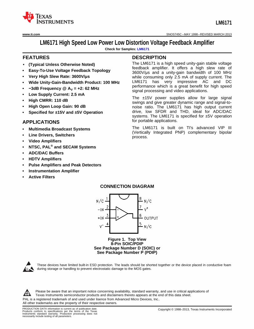
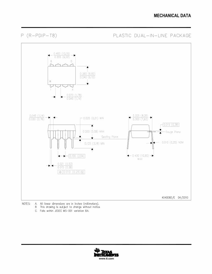
CONNECTION DIAGRAM
Figure 1. Top View8-Pin SOIC/PDIP
See Package Number D (SOIC) orSee Package Number P (PDIP)
These devices have limited built-in ESD protection. The leads should be shorted together or the device placed in conductive foamduring storage or handling to prevent electrostatic damage to the MOS gates.
1
Please be aware that an important notice concerning availability, standard warranty, and use in critical applications ofTexas Instruments semiconductor products and disclaimers thereto appears at the end of this data sheet.
2PAL is a registered trademark of and used under lisence from Advanced Micro Devices, Inc..3All other trademarks are the property of their respective owners.
Soldering Information Infrared or Convection Reflow 235°C(20 sec.)
Wave Soldering Lead Temp 260°C(10 sec.)
(1) If Military/Aerospace specified devices are required, please contact the Texas Instruments Sales Office/Distributors for availability andspecifications.
(2) Absolute Maximum Ratings indicate limits beyond which damage to the device may occur. Operating Ratings indicate conditions forwhich the device is intended to be functional, but specific performance is not guaranteed. For guaranteed specifications and the testconditions, see the Electrical Characteristics.
(3) Human body model, 1.5 kΩ in series with 100 pF.(4) Continuous short circuit operation at elevated ambient temperature can result in exceeding the maximum allowed junction temperature
of 150°C.(5) The maximum power dissipation is a function of TJ(max), θJA, and TA. The maximum allowable power dissipation at any ambient
temperature is PD = (TJ(max) − TA)/θJA. All numbers apply for packages soldered directly into a PC board.
Operating Ratings (1)
Supply Voltage 5.5V ≤ VS ≤ 34V
Operating Temperature Range LM6171AI, LM6171BI −40°C to +85°C
Thermal Resistance (θJA) P Package, 8-Pin PDIP 108°C/W
D Package, 8-Pin SOIC 172°C/W
(1) Absolute Maximum Ratings indicate limits beyond which damage to the device may occur. Operating Ratings indicate conditions forwhich the device is intended to be functional, but specific performance is not guaranteed. For guaranteed specifications and the testconditions, see the Electrical Characteristics.
±15V DC Electrical CharacteristicsUnless otherwise specified, all limits guaranteed for TJ = 25°C, V+ = +15V, V− = −15V, VCM = 0V, and RL = 1 kΩ. Boldfacelimits apply at the temperature extremes
Symbol Parameter Conditions Typ LM6171AI LM6171BI Units(1) Limit Limit
(2) (2)
VOS Input Offset Voltage 1.5 3 6 mV
5 8 max
TC VOS Input Offset Voltage Average Drift 6 μV/°C
IB Input Bias Current 1 3 3 μA
4 4 max
IOS Input Offset Current 0.03 2 2 μA
3 3 max
RIN Input Resistance Common Mode 40MΩ
Differential Mode 4.9
RO Open Loop Output Resistance 14 ΩCMRR Common Mode Rejection Ratio VCM = ±10V 110 80 75 dB
75 70 min
PSRR Power Supply Rejection Ratio VS = ±15V to ±5V 95 85 80 dB
80 75 min
VCM Input Common-Mode Voltage Range CMRR ≥ 60 dB ±13.5 V
AV Large Signal Voltage Gain (3) RL = 1 kΩ 90 80 80 dB
70 70 min
RL = 100Ω 83 70 70 dB
60 60 min
VO Output Swing RL = 1 kΩ 13.3 12.5 12.5 V
12 12 min
−13.3 −12.5 −12.5 V
−12 −12 max
RL = 100Ω 11.6 9 9 V
8.5 8.5 min
−10.5 −9 −9 V
−8.5 −8.5 max
Continuous Output Current (Open Loop) (4) Sourcing, RL = 100Ω 116 90 90 mA
85 85 min
Sinking, RL = 100Ω 105 90 90 mA
85 85 max
Continuous Output Current (in Linear Sourcing, RL = 10Ω 100 mARegion) Sinking, RL = 10Ω 80 mA
ISC Output Short Circuit Current Sourcing 135 mA
Sinking 135 mA
IS Supply Current 2.5 4 4 mA
4.5 4.5 max
(1) Typical Values represent the most likely parametric norm.(2) All limits are guaranteed by testing or statistical analysis.(3) Large signal voltage gain is the total output swing divided by the input signal required to produce that swing. For VS = ±15V, VOUT =
±5V. For VS = +5V, VOUT = ±1V.(4) The open loop output current is the output swing with the 100Ω load resistor divided by that resistor.
±15V AC Electrical CharacteristicsUnless otherwise specified, all limits guaranteed for TJ = 25°C, V+ = +15V, V− = −15V, VCM = 0V, and RL = 1 kΩ. Boldfacelimits apply at the temperature extremes
Symbol Parameter Conditions Typ LM6171AI LM6171BI Units(1) Limit Limit
(2) (2)
SR Slew Rate (3) AV = +2, VIN = 13 VPP 3600 V/μs
AV = +2, VIN = 10 VPP 3000
GBW Unity Gain-Bandwidth Product 100 MHz
−3 dB Frequency AV = +1 160 MHz
AV = +2 62 MHz
φm Phase Margin 40 deg
ts Settling Time (0.1%) AV = −1, VOUT = ±5V RL = 48 ns500ΩPropagation Delay VIN = ±5V, RL = 500Ω, AV = 6 ns−2
AD Differential Gain (4) 0.03 %
φD Differential Phase (4) 0.5 deg
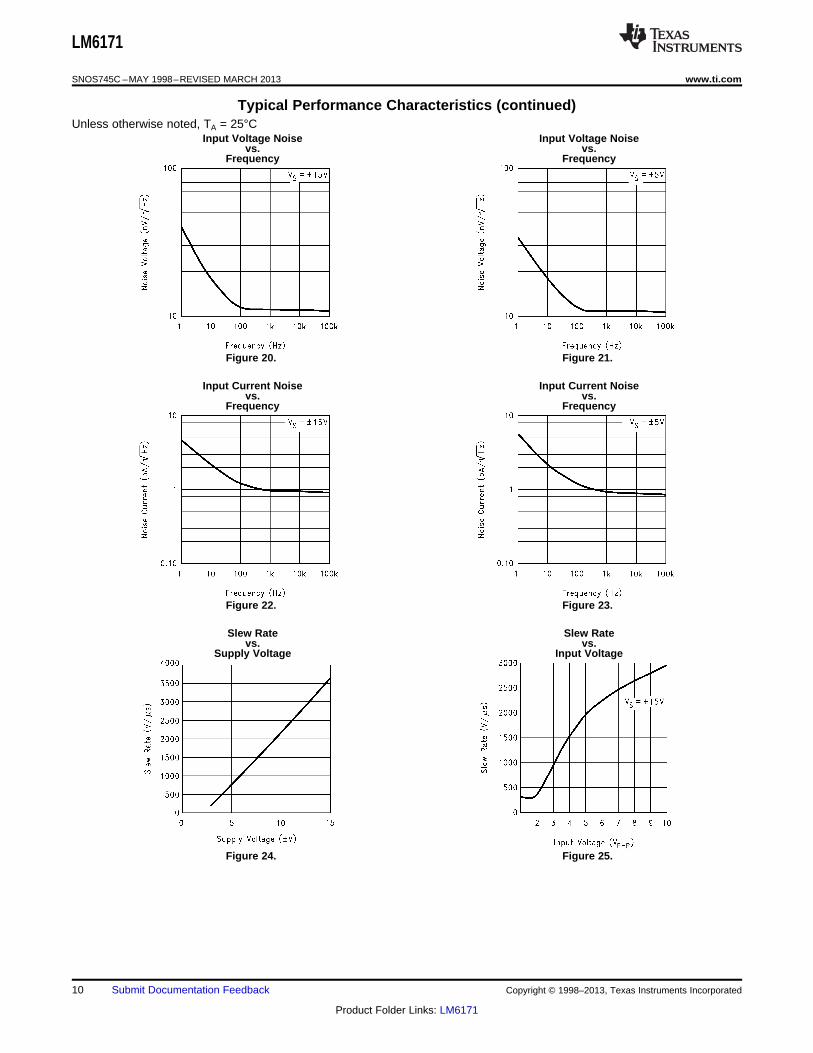
en Input-Referred Voltage Noise f = 1 kHz 12 nV/√Hz
in Input-Referred Current Noise f = 1 kHz 1 pA/√Hz
(1) Typical Values represent the most likely parametric norm.(2) All limits are guaranteed by testing or statistical analysis.(3) Slew rate is the average of the rising and falling slew rates.(4) Differential gain and phase are measured with AV = +2, VIN = 1 VPP at 3.58 MHz and both input and output 75Ω terminated.
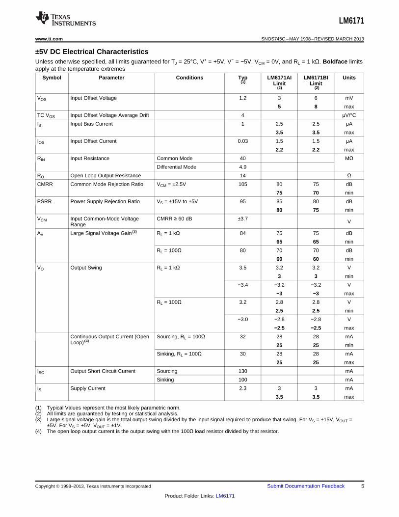
±5V DC Electrical CharacteristicsUnless otherwise specified, all limits guaranteed for TJ = 25°C, V+ = +5V, V− = −5V, VCM = 0V, and RL = 1 kΩ. Boldface limitsapply at the temperature extremes
Symbol Parameter Conditions Typ LM6171AI LM6171BI Units(1) Limit Limit
(2) (2)
VOS Input Offset Voltage 1.2 3 6 mV
5 8 max
TC VOS Input Offset Voltage Average Drift 4 μV/°C
IB Input Bias Current 1 2.5 2.5 μA
3.5 3.5 max
IOS Input Offset Current 0.03 1.5 1.5 μA
2.2 2.2 max
RIN Input Resistance Common Mode 40 MΩDifferential Mode 4.9
RO Open Loop Output Resistance 14 ΩCMRR Common Mode Rejection Ratio VCM = ±2.5V 105 80 75 dB
75 70 min
PSRR Power Supply Rejection Ratio VS = ±15V to ±5V 95 85 80 dB
80 75 min
VCM Input Common-Mode Voltage CMRR ≥ 60 dB ±3.7 VRange
AV Large Signal Voltage Gain (3) RL = 1 kΩ 84 75 75 dB
(1) Typical Values represent the most likely parametric norm.(2) All limits are guaranteed by testing or statistical analysis.(3) Large signal voltage gain is the total output swing divided by the input signal required to produce that swing. For VS = ±15V, VOUT =
±5V. For VS = +5V, VOUT = ±1V.(4) The open loop output current is the output swing with the 100Ω load resistor divided by that resistor.
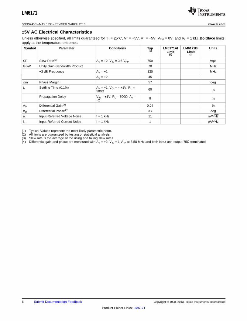
±5V AC Electrical CharacteristicsUnless otherwise specified, all limits guaranteed for TJ = 25°C, V+ = +5V, V− = −5V, VCM = 0V, and RL = 1 kΩ. Boldface limitsapply at the temperature extremes
Symbol Parameter Conditions Typ LM6171AI LM6171BI Units(1) Limit Limit
(2) (2)
SR Slew Rate (3) AV = +2, VIN = 3.5 VPP 750 V/μs
GBW Unity Gain-Bandwidth Product 70 MHz
−3 dB Frequency AV = +1 130 MHz
AV = +2 45
φm Phase Margin 57 deg
ts Settling Time (0.1%) AV = −1, VOUT = +1V, RL = 60 ns500ΩPropagation Delay VIN = ±1V, RL = 500Ω, AV = 8 ns−2
AD Differential Gain (4) 0.04 %
φD Differential Phase (4) 0.7 deg
en Input-Referred Voltage Noise f = 1 kHz 11 nV/√Hz
in Input-Referred Current Noise f = 1 kHz 1 pA/√Hz
(1) Typical Values represent the most likely parametric norm.(2) All limits are guaranteed by testing or statistical analysis.(3) Slew rate is the average of the rising and falling slew rates.(4) Differential gain and phase are measured with AV = +2, VIN = 1 VPP at 3.58 MHz and both input and output 75Ω terminated.
The LM6171 is a high speed, unity-gain stable voltage feedback amplifier. It consumes only 2.5 mA supplycurrent while providing a gain-bandwidth product of 100 MHz and a slew rate of 3600V/μs. It also has other greatfeatures such as low differential gain and phase and high output current. The LM6171 is a good choice in highspeed circuits.
The LM6171 is a true voltage feedback amplifier. Unlike current feedback amplifiers (CFAs) with a low invertinginput impedance and a high non-inverting input impedance, both inputs of voltage feedback amplifiers (VFAs)have high impedance nodes. The low impedance inverting input in CFAs will couple with feedback capacitor andcause oscillation. As a result, CFAs cannot be used in traditional op amp circuits such as photodiode amplifiers,I-to-V converters and integrators.
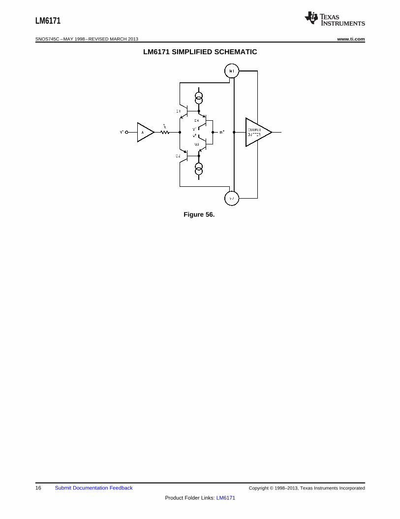
LM6171 CIRCUIT OPERATION
The class AB input stage in LM6171 is fully symmetrical and has a similar slewing characteristic to the currentfeedback amplifiers. In LM6171 Figure 56, Q1 through Q4 form the equivalent of the current feedback inputbuffer, RE the equivalent of the feedback resistor, and stage A buffers the inverting input. The triple-bufferedoutput stage isolates the gain stage from the load to provide low output impedance.
LM6171 SLEW RATE CHARACTERISTIC
The slew rate of LM6171 is determined by the current available to charge and discharge an internal highimpedance node capacitor. The current is the differential input voltage divided by the total degeneration resistorRE. Therefore, the slew rate is proportional to the input voltage level, and the higher slew rates are achievable inthe lower gain configurations.
When a very fast large signal pulse is applied to the input of an amplifier, some overshoot or undershoot occurs.By placing an external series resistor such as 1 kΩ to the input of LM6171, the bandwidth is reduced to helplower the overshoot.
LAYOUT CONSIDERATION
Printed Circuit Boards and High Speed Op Amps
There are many things to consider when designing PC boards for high speed op amps. Without proper caution, itis very easy and frustrating to have excessive ringing, oscillation and other degraded AC performance in highspeed circuits. As a rule, the signal traces should be short and wide to provide low inductance and lowimpedance paths. Any unused board space needs to be grounded to reduce stray signal pickup. Criticalcomponents should also be grounded at a common point to eliminate voltage drop. Sockets add capacitance tothe board and can affect frequency performance. It is better to solder the amplifier directly into the PC boardwithout using any socket.
Using Probes
Active (FET) probes are ideal for taking high frequency measurements because they have wide bandwidth, highinput impedance and low input capacitance. However, the probe ground leads provide a long ground loop thatwill produce errors in measurement. Instead, the probes can be grounded directly by removing the ground leadsand probe jackets and using scope probe jacks.
Components Selection And Feedback Resistor
It is important in high speed applications to keep all component leads short because wires are inductive at highfrequency. For discrete components, choose carbon composition-type resistors and mica-type capacitors.Surface mount components are preferred over discrete components for minimum inductive effect.
Large values of feedback resistors can couple with parasitic capacitance and cause undesirable effects such asringing or oscillation in high speed amplifiers. For LM6171, a feedback resistor of 510Ω gives optimalperformance.
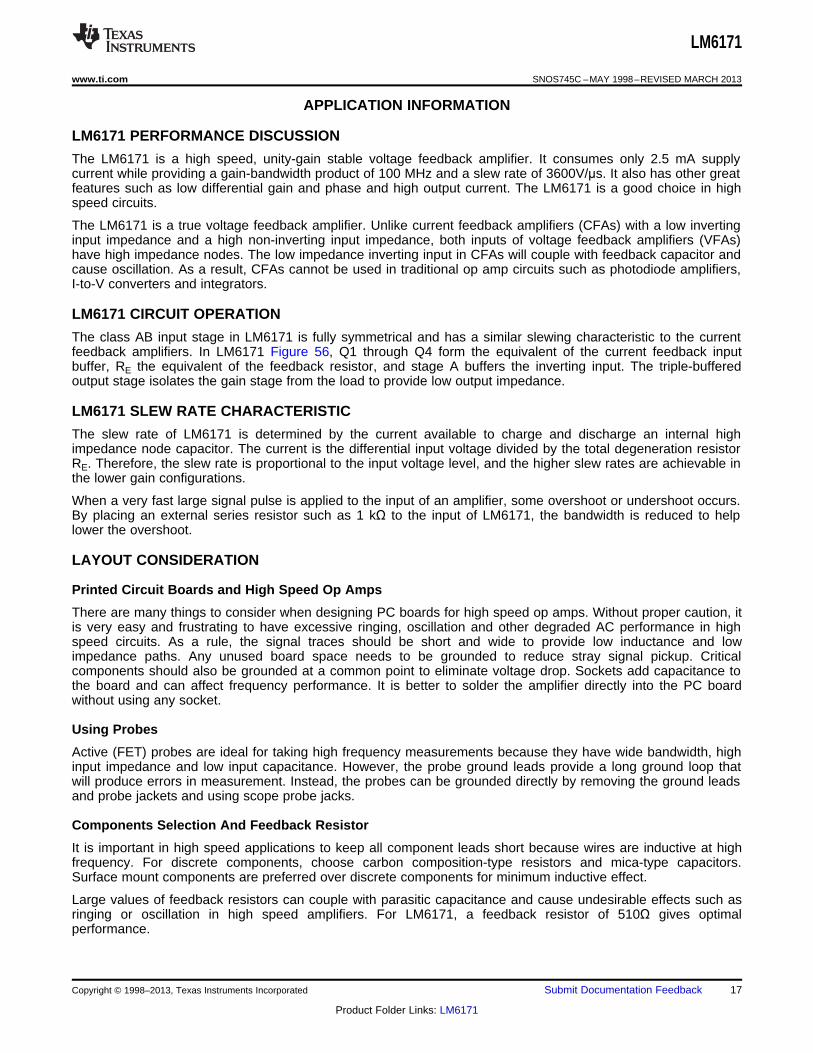
The combination of an amplifier's input capacitance with the gain setting resistors adds a pole that can causepeaking or oscillation. To solve this problem, a feedback capacitor with a value
CF > (RG × CIN)/RF (1)
can be used to cancel that pole. For LM6171, a feedback capacitor of 2 pF is recommended. Figure 57 illustratesthe compensation circuit.
Figure 57. Compensating for Input Capacitance
POWER SUPPLY BYPASSING
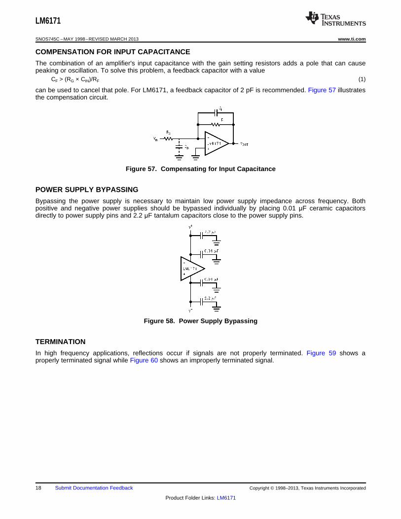
Bypassing the power supply is necessary to maintain low power supply impedance across frequency. Bothpositive and negative power supplies should be bypassed individually by placing 0.01 μF ceramic capacitorsdirectly to power supply pins and 2.2 μF tantalum capacitors close to the power supply pins.
Figure 58. Power Supply Bypassing
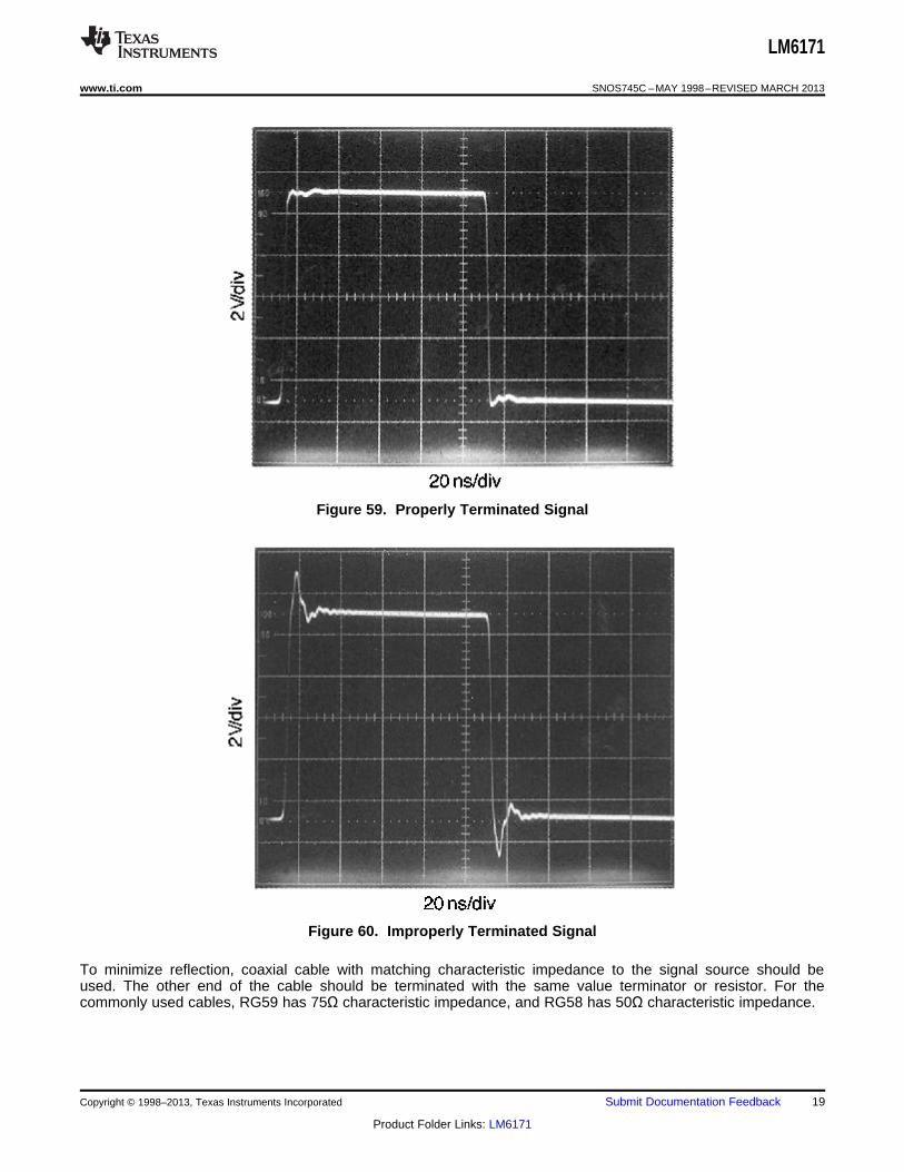
TERMINATION
In high frequency applications, reflections occur if signals are not properly terminated. Figure 59 shows aproperly terminated signal while Figure 60 shows an improperly terminated signal.
To minimize reflection, coaxial cable with matching characteristic impedance to the signal source should beused. The other end of the cable should be terminated with the same value terminator or resistor. For thecommonly used cables, RG59 has 75Ω characteristic impedance, and RG58 has 50Ω characteristic impedance.
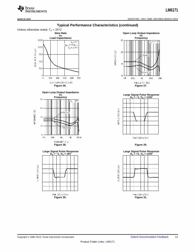
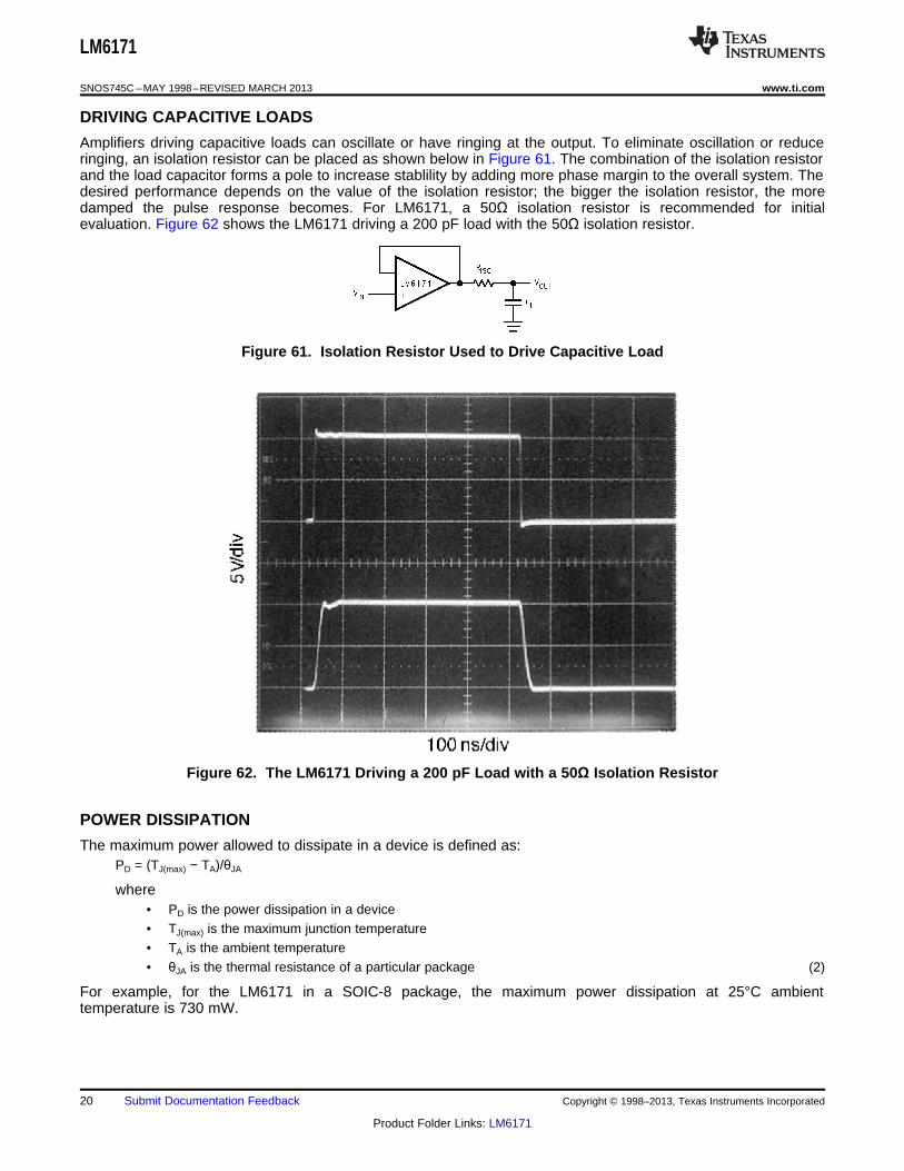
Amplifiers driving capacitive loads can oscillate or have ringing at the output. To eliminate oscillation or reduceringing, an isolation resistor can be placed as shown below in Figure 61. The combination of the isolation resistorand the load capacitor forms a pole to increase stablility by adding more phase margin to the overall system. Thedesired performance depends on the value of the isolation resistor; the bigger the isolation resistor, the moredamped the pulse response becomes. For LM6171, a 50Ω isolation resistor is recommended for initialevaluation. Figure 62 shows the LM6171 driving a 200 pF load with the 50Ω isolation resistor.
Figure 61. Isolation Resistor Used to Drive Capacitive Load
Figure 62. The LM6171 Driving a 200 pF Load with a 50Ω Isolation Resistor
POWER DISSIPATION
The maximum power allowed to dissipate in a device is defined as:PD = (TJ(max) − TA)/θJA
where• PD is the power dissipation in a device• TJ(max) is the maximum junction temperature• TA is the ambient temperature• θJA is the thermal resistance of a particular package (2)
For example, for the LM6171 in a SOIC-8 package, the maximum power dissipation at 25°C ambienttemperature is 730 mW.
Thermal resistance, θJA, depends on parameters such as die size, package size and package material. Thesmaller the die size and package, the higher θJA becomes. The 8-pin PDIP package has a lower thermalresistance (108°C/W) than that of 8-pin SOIC-8 (172°C/W). Therefore, for higher dissipation capability, use an 8-pin PDIP package.
The total power dissipated in a device can be calculated as:PD = PQ + PL (3)
PQ is the quiescent power dissipated in a device with no load connected at the output. PL is the power dissipatedin the device with a load connected at the output; it is not the power dissipated by the load.
Furthermore,
PQ = supply current × total supply voltage with no load
PL = output current × (voltage difference between supply voltage and output voltage of the same supply)
For example, the total power dissipated by the LM6171 with VS = ±15V and output voltage of 10V into 1 kΩ loadresistor (one end tied to ground) is
Changes from Revision B (March 2013) to Revision C Page
• Changed layout of National Data Sheet to TI format .......................................................................................................... 21
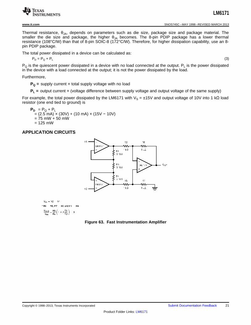
LM6171AIM NRND SOIC D 8 95 TBD Call TI Call TI -40 to 85 LM6171AIM
LM6171AIM/NOPB ACTIVE SOIC D 8 95 Green (RoHS& no Sb/Br)
CU SN Level-1-260C-UNLIM -40 to 85 LM6171AIM
LM6171AIMX/NOPB ACTIVE SOIC D 8 2500 Green (RoHS& no Sb/Br)
CU SN Level-1-260C-UNLIM -40 to 85 LM6171AIM
LM6171BIM NRND SOIC D 8 95 TBD Call TI Call TI -40 to 85 LM6171BIM
LM6171BIM/NOPB ACTIVE SOIC D 8 95 Green (RoHS& no Sb/Br)
CU SN Level-1-260C-UNLIM -40 to 85 LM6171BIM
LM6171BIMX/NOPB ACTIVE SOIC D 8 2500 Green (RoHS& no Sb/Br)
CU SN Level-1-260C-UNLIM -40 to 85 LM6171BIM
LM6171BIN/NOPB ACTIVE PDIP P 8 40 Green (RoHS& no Sb/Br)
CU SN Level-1-NA-UNLIM -40 to 85 LM6171BIN
(1) The marketing status values are defined as follows:ACTIVE: Product device recommended for new designs.LIFEBUY: TI has announced that the device will be discontinued, and a lifetime-buy period is in effect.NRND: Not recommended for new designs. Device is in production to support existing customers, but TI does not recommend using this part in a new design.PREVIEW: Device has been announced but is not in production. Samples may or may not be available.OBSOLETE: TI has discontinued the production of the device.
(2) RoHS: TI defines "RoHS" to mean semiconductor products that are compliant with the current EU RoHS requirements for all 10 RoHS substances, including the requirement that RoHS substancedo not exceed 0.1% by weight in homogeneous materials. Where designed to be soldered at high temperatures, "RoHS" products are suitable for use in specified lead-free processes. TI mayreference these types of products as "Pb-Free".RoHS Exempt: TI defines "RoHS Exempt" to mean products that contain lead but are compliant with EU RoHS pursuant to a specific EU RoHS exemption.Green: TI defines "Green" to mean the content of Chlorine (Cl) and Bromine (Br) based flame retardants meet JS709B low halogen requirements of <=1000ppm threshold. Antimony trioxide basedflame retardants must also meet the <=1000ppm threshold requirement.
(3) MSL, Peak Temp. - The Moisture Sensitivity Level rating according to the JEDEC industry standard classifications, and peak solder temperature.
(4) There may be additional marking, which relates to the logo, the lot trace code information, or the environmental category on the device.
(5) Multiple Device Markings will be inside parentheses. Only one Device Marking contained in parentheses and separated by a "~" will appear on a device. If a line is indented then it is a continuationof the previous line and the two combined represent the entire Device Marking for that device.
(6) Lead/Ball Finish - Orderable Devices may have multiple material finish options. Finish options are separated by a vertical ruled line. Lead/Ball Finish values may wrap to two lines if the finishvalue exceeds the maximum column width.
Important Information and Disclaimer:The information provided on this page represents TI's knowledge and belief as of the date that it is provided. TI bases its knowledge and belief on informationprovided by third parties, and makes no representation or warranty as to the accuracy of such information. Efforts are underway to better integrate information from third parties. TI has taken andcontinues to take reasonable steps to provide representative and accurate information but may not have conducted destructive testing or chemical analysis on incoming materials and chemicals.TI and TI suppliers consider certain information to be proprietary, and thus CAS numbers and other limited information may not be available for release.
In no event shall TI's liability arising out of such information exceed the total purchase price of the TI part(s) at issue in this document sold by TI to Customer on an annual basis.
Texas Instruments Incorporated (TI) reserves the right to make corrections, enhancements, improvements and other changes to itssemiconductor products and services per JESD46, latest issue, and to discontinue any product or service per JESD48, latest issue. Buyersshould obtain the latest relevant information before placing orders and should verify that such information is current and complete.TI’s published terms of sale for semiconductor products (http://www.ti.com/sc/docs/stdterms.htm) apply to the sale of packaged integratedcircuit products that TI has qualified and released to market. Additional terms may apply to the use or sale of other types of TI products andservices.Reproduction of significant portions of TI information in TI data sheets is permissible only if reproduction is without alteration and isaccompanied by all associated warranties, conditions, limitations, and notices. TI is not responsible or liable for such reproduceddocumentation. Information of third parties may be subject to additional restrictions. Resale of TI products or services with statementsdifferent from or beyond the parameters stated by TI for that product or service voids all express and any implied warranties for theassociated TI product or service and is an unfair and deceptive business practice. TI is not responsible or liable for any such statements.Buyers and others who are developing systems that incorporate TI products (collectively, “Designers”) understand and agree that Designersremain responsible for using their independent analysis, evaluation and judgment in designing their applications and that Designers havefull and exclusive responsibility to assure the safety of Designers' applications and compliance of their applications (and of all TI productsused in or for Designers’ applications) with all applicable regulations, laws and other applicable requirements. Designer represents that, withrespect to their applications, Designer has all the necessary expertise to create and implement safeguards that (1) anticipate dangerousconsequences of failures, (2) monitor failures and their consequences, and (3) lessen the likelihood of failures that might cause harm andtake appropriate actions. Designer agrees that prior to using or distributing any applications that include TI products, Designer willthoroughly test such applications and the functionality of such TI products as used in such applications.TI’s provision of technical, application or other design advice, quality characterization, reliability data or other services or information,including, but not limited to, reference designs and materials relating to evaluation modules, (collectively, “TI Resources”) are intended toassist designers who are developing applications that incorporate TI products; by downloading, accessing or using TI Resources in anyway, Designer (individually or, if Designer is acting on behalf of a company, Designer’s company) agrees to use any particular TI Resourcesolely for this purpose and subject to the terms of this Notice.TI’s provision of TI Resources does not expand or otherwise alter TI’s applicable published warranties or warranty disclaimers for TIproducts, and no additional obligations or liabilities arise from TI providing such TI Resources. TI reserves the right to make corrections,enhancements, improvements and other changes to its TI Resources. TI has not conducted any testing other than that specificallydescribed in the published documentation for a particular TI Resource.Designer is authorized to use, copy and modify any individual TI Resource only in connection with the development of applications thatinclude the TI product(s) identified in such TI Resource. NO OTHER LICENSE, EXPRESS OR IMPLIED, BY ESTOPPEL OR OTHERWISETO ANY OTHER TI INTELLECTUAL PROPERTY RIGHT, AND NO LICENSE TO ANY TECHNOLOGY OR INTELLECTUAL PROPERTYRIGHT OF TI OR ANY THIRD PARTY IS GRANTED HEREIN, including but not limited to any patent right, copyright, mask work right, orother intellectual property right relating to any combination, machine, or process in which TI products or services are used. Informationregarding or referencing third-party products or services does not constitute a license to use such products or services, or a warranty orendorsement thereof. Use of TI Resources may require a license from a third party under the patents or other intellectual property of thethird party, or a license from TI under the patents or other intellectual property of TI.TI RESOURCES ARE PROVIDED “AS IS” AND WITH ALL FAULTS. TI DISCLAIMS ALL OTHER WARRANTIES ORREPRESENTATIONS, EXPRESS OR IMPLIED, REGARDING RESOURCES OR USE THEREOF, INCLUDING BUT NOT LIMITED TOACCURACY OR COMPLETENESS, TITLE, ANY EPIDEMIC FAILURE WARRANTY AND ANY IMPLIED WARRANTIES OFMERCHANTABILITY, FITNESS FOR A PARTICULAR PURPOSE, AND NON-INFRINGEMENT OF ANY THIRD PARTY INTELLECTUALPROPERTY RIGHTS. TI SHALL NOT BE LIABLE FOR AND SHALL NOT DEFEND OR INDEMNIFY DESIGNER AGAINST ANY CLAIM,INCLUDING BUT NOT LIMITED TO ANY INFRINGEMENT CLAIM THAT RELATES TO OR IS BASED ON ANY COMBINATION OFPRODUCTS EVEN IF DESCRIBED IN TI RESOURCES OR OTHERWISE. IN NO EVENT SHALL TI BE LIABLE FOR ANY ACTUAL,DIRECT, SPECIAL, COLLATERAL, INDIRECT, PUNITIVE, INCIDENTAL, CONSEQUENTIAL OR EXEMPLARY DAMAGES INCONNECTION WITH OR ARISING OUT OF TI RESOURCES OR USE THEREOF, AND REGARDLESS OF WHETHER TI HAS BEENADVISED OF THE POSSIBILITY OF SUCH DAMAGES.Unless TI has explicitly designated an individual product as meeting the requirements of a particular industry standard (e.g., ISO/TS 16949and ISO 26262), TI is not responsible for any failure to meet such industry standard requirements.Where TI specifically promotes products as facilitating functional safety or as compliant with industry functional safety standards, suchproducts are intended to help enable customers to design and create their own applications that meet applicable functional safety standardsand requirements. Using products in an application does not by itself establish any safety features in the application. Designers mustensure compliance with safety-related requirements and standards applicable to their applications. Designer may not use any TI products inlife-critical medical equipment unless authorized officers of the parties have executed a special contract specifically governing such use.Life-critical medical equipment is medical equipment where failure of such equipment would cause serious bodily injury or death (e.g., lifesupport, pacemakers, defibrillators, heart pumps, neurostimulators, and implantables). Such equipment includes, without limitation, allmedical devices identified by the U.S. Food and Drug Administration as Class III devices and equivalent classifications outside the U.S.TI may expressly designate certain products as completing a particular qualification (e.g., Q100, Military Grade, or Enhanced Product).Designers agree that it has the necessary expertise to select the product with the appropriate qualification designation for their applicationsand that proper product selection is at Designers’ own risk. Designers are solely responsible for compliance with all legal and regulatoryrequirements in connection with such selection.Designer will fully indemnify TI and its representatives against any damages, costs, losses, and/or liabilities arising out of Designer’s non-compliance with the terms and provisions of this Notice.