LM833Dual Audio Operational AmplifierGeneral DescriptionThe LM833 is a dual general purpose operational amplifierdesigned with particular emphasis on performance in audiosystems.
This dual amplifier IC utilizes new circuit and processingtechniques to deliver low noise, high speed and wide band-width without increasing external components or decreasingstability. The LM833 is internally compensated for all closedloop gains and is therefore optimized for all preamp and highlevel stages in PCM and HiFi systems.
The LM833 is pin-for-pin compatible with industry standarddual operational amplifiers.
Featuresj Wide dynamic range: 140dB
j Low input noisevoltage: 4.5nV/√Hz
j High slew rate: 7 V/µs (typ); 5V/µs (min)
j High gain bandwidth: 15MHz (typ); 10MHz (min)
j Wide power bandwidth: 120KHz
j Low distortion: 0.002%
j Low offset voltage: 0.3mV
j Large phase margin: 60˚
j Available in 8 pinMSOP package
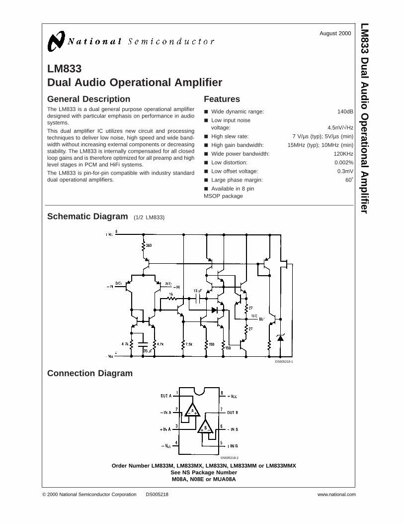
Schematic Diagram (1/2 LM833)
Connection Diagram
DS005218-1
DS005218-2
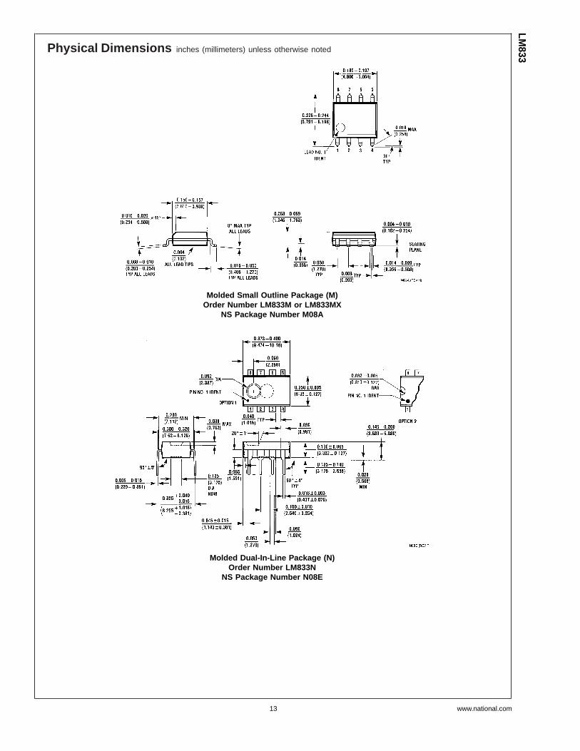
Order Number LM833M, LM833MX, LM833N, LM833MM or LM833MMXSee NS Package NumberM08A, N08E or MUA08A
If Military/Aerospace specified devices are required,please contact the National Semiconductor Sales Office/Distributors for availability and specifications.
Supply Voltage VCC–VEE 36VDifferential Input Voltage (Note 3) VI ±30VInput Voltage Range (Note 3) VIC ±15VPower Dissipation (Note 4) PD 500 mWOperating Temperature Range TOPR −40 ∼ 85˚CStorage Temperature Range TSTG −60 ∼ 150˚C
Soldering InformationDual-In-Line Package
Soldering (10 seconds) 260˚CSmall Outline Package(SOIC and MSOP)
See AN-450 “Surface Mounting Methods and Their Effecton Product Reliability” for other methods of solderingsurface mount devices.ESD tolerance (Note 5) 1600V
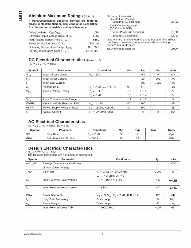
DC Electrical Characteristics (Notes 1, 2)(TA = 25˚C, VS = ±15V)
Symbol Parameter Conditions Min Typ Max Units
VOS Input Offset Voltage RS = 10Ω 0.3 5 mV
IOS Input Offset Current 10 200 nA
IB Input Bias Current 500 1000 nA
AV Voltage Gain RL = 2 kΩ, VO = ±10V 90 110 dB
VOM Output Voltage Swing RL = 10 kΩ ±12 ±13.5 V
RL = 2 kΩ ±10 ±13.4 V
VCM Input Common-Mode Range ±12 ±14.0 V
CMRR Common-Mode Rejection Ratio VIN = ±12V 80 100 dB
PSRR Power Supply Rejection Ratio VS = 15∼5V, −15∼−5V 80 100 dB
IQ Supply Current VO = 0V, Both Amps 5 8 mA
AC Electrical Characteristics(TA = 25˚C, VS = ±15V, RL = 2 kΩ)
Symbol Parameter Conditions Min Typ Max Units
SR Slew Rate RL = 2 kΩ 5 7 V/µs
GBW Gain Bandwidth Product f = 100 kHz 10 15 MHz
Design Electrical Characteristics(TA = 25˚C, VS = ±15V)The following parameters are not tested or guaranteed.
Symbol Parameter Conditions Typ Units
∆VOS/∆T Average Temperature Coefficient 2 µV/˚C
of Input Offset Voltage
THD Distortion RL = 2 kΩ, f = 20∼20 kHz 0.002 %
VOUT = 3 Vrms, AV = 1
en Input Referred Noise Voltage RS = 100Ω, f = 1 kHz 4.5
in Input Referred Noise Current f = 1 kHz 0.7
PBW Power Bandwidth VO = 27 Vpp, RL = 2 kΩ, THD ≤ 1% 120 kHz
fU Unity Gain Frequency Open Loop 9 MHz
φM Phase Margin Open Loop 60 deg
Input Referred Cross Talk f = 20∼20 kHz −120 dB
LM83
3
www.national.com 2
Design Electrical Characteristics (Continued)
Note 1: Absolute Maximum Ratings indicate limits beyond which damage to the device may occur. Operating Ratings indicate conditions for which the device is func-tional, but do not guarantee specific performance limits. Electrical Characteristics state DC and AC electrical specifications under particular test conditions which guar-antee specific performance limits. This assumes that the device is within the Operating Ratings. Specifications are not guaranteed for parameters where no limit isgiven, however, the typical value is a good indication of device performance.
Note 2: All voltages are measured with respect to the ground pin, unless otherwise specified.
Note 3: If supply voltage is less than ±15V, it is equal to supply voltage.
Note 4: This is the permissible value at TA ≤ 85˚C.
Note 5: Human body model, 1.5 kΩ in series with 100 pF.
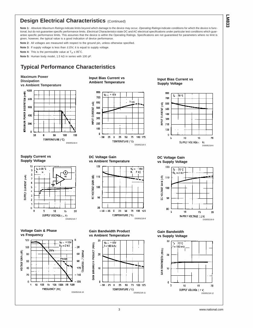
Typical Performance Characteristics
Maximum PowerDissipationvs Ambient Temperature
DS005218-4
Input Bias Current vsAmbient Temperature
DS005218-5
Input Bias Current vsSupply Voltage
DS005218-6
Supply Current vsSupply Voltage
DS005218-7
DC Voltage Gainvs Ambient Temperature
DS005218-8
DC Voltage Gainvs Supply Voltage
DS005218-9
Voltage Gain & Phasevs Frequency
DS005218-10
Gain Bandwidth Productvs Ambient Temperature
DS005218-11
Gain Bandwidthvs Supply Voltage
DS005218-12
LM833
www.national.com3
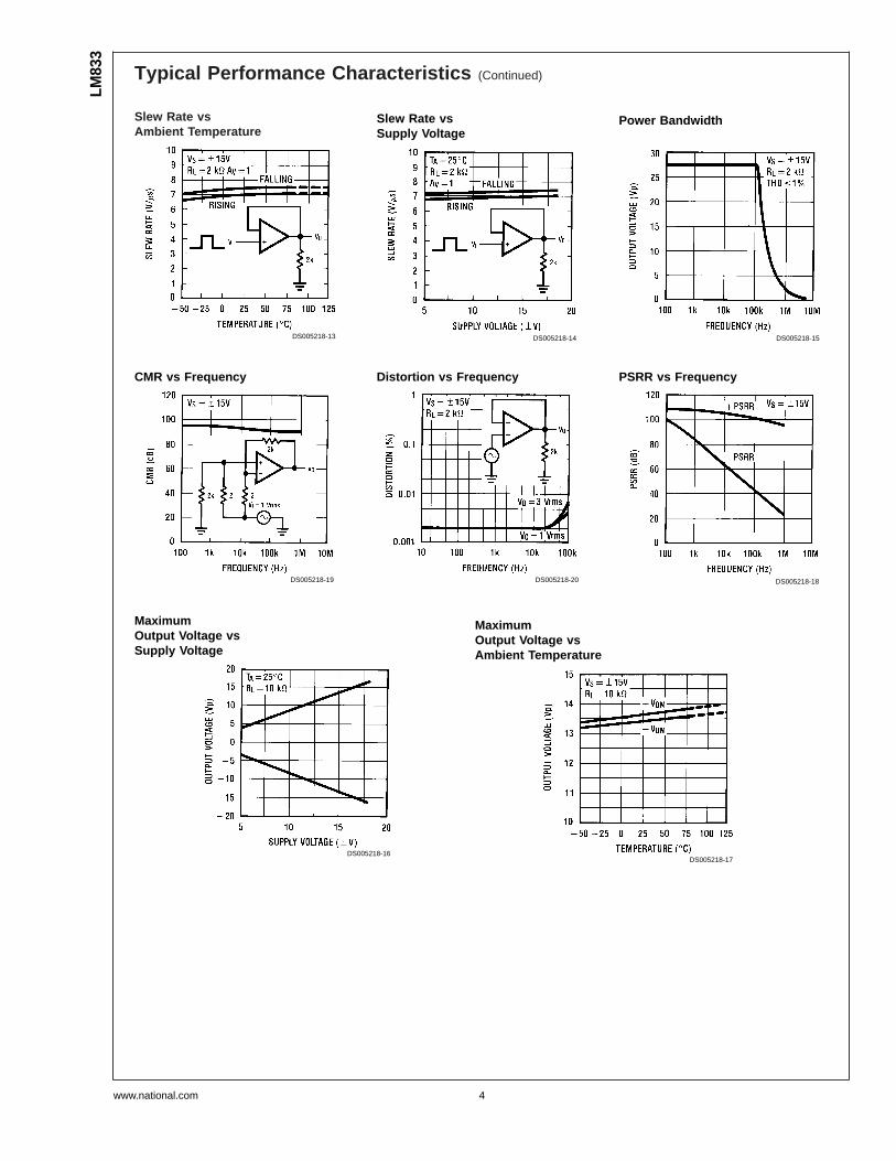
Typical Performance Characteristics (Continued)
Slew Rate vsAmbient Temperature
DS005218-13
Slew Rate vsSupply Voltage
DS005218-14
Power Bandwidth
DS005218-15
CMR vs Frequency
DS005218-19
Distortion vs Frequency
DS005218-20
PSRR vs Frequency
DS005218-18
MaximumOutput Voltage vsSupply Voltage
DS005218-16
MaximumOutput Voltage vsAmbient Temperature
DS005218-17
LM83
3
www.national.com 4
Typical Performance Characteristics (Continued)
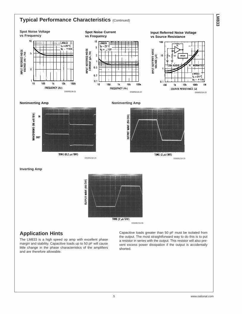
Application HintsThe LM833 is a high speed op amp with excellent phasemargin and stability. Capacitive loads up to 50 pF will causelittle change in the phase characteristics of the amplifiersand are therefore allowable.
Capacitive loads greater than 50 pF must be isolated fromthe output. The most straightforward way to do this is to puta resistor in series with the output. This resistor will also pre-vent excess power dissipation if the output is accidentallyshorted.
Spot Noise Voltagevs Frequency
DS005218-21
Spot Noise Currentvs Frequency
DS005218-22
Input Referred Noise Voltagevs Source Resistance
DS005218-23
Noninverting Amp
DS005218-24
Noninverting Amp
DS005218-25
Inverting Amp
DS005218-26
LM833
www.national.com5
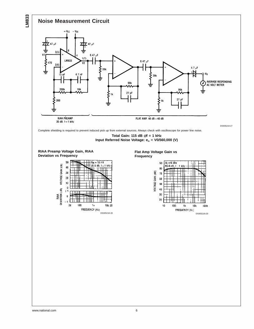
Noise Measurement Circuit
DS005218-27
Complete shielding is required to prevent induced pick up from external sources. Always check with oscilloscope for power line noise.
Total Gain: 115 dB @f = 1 kHzInput Referred Noise Voltage: e n = V0/560,000 (V)
RIAA Preamp Voltage Gain, RIAADeviation vs Frequency
NATIONAL’S PRODUCTS ARE NOT AUTHORIZED FOR USE AS CRITICAL COMPONENTS IN LIFE SUPPORTDEVICES OR SYSTEMS WITHOUT THE EXPRESS WRITTEN APPROVAL OF THE PRESIDENT AND GENERALCOUNSEL OF NATIONAL SEMICONDUCTOR CORPORATION. As used herein:
1. Life support devices or systems are devices orsystems which, (a) are intended for surgical implantinto the body, or (b) support or sustain life, andwhose failure to perform when properly used inaccordance with instructions for use provided in thelabeling, can be reasonably expected to result in asignificant injury to the user.
2. A critical component is any component of a lifesupport device or system whose failure to performcan be reasonably expected to cause the failure ofthe life support device or system, or to affect itssafety or effectiveness.
National SemiconductorCorporationAmericasTel: 1-800-272-9959Fax: 1-800-737-7018Email: [email protected]
National SemiconductorAsia Pacific CustomerResponse GroupTel: 65-2544466Fax: 65-2504466Email: [email protected]
National SemiconductorJapan Ltd.Tel: 81-3-5639-7560Email: [email protected]: 81-3-5639-7507
www.national.com
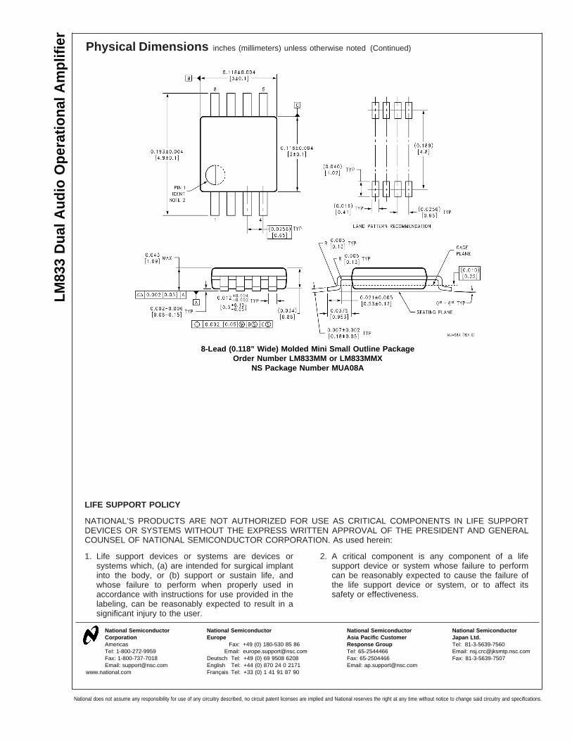
8-Lead (0.118” Wide) Molded Mini Small Outline PackageOrder Number LM833MM or LM833MMX
NS Package Number MUA08A
LM83
3D
ualA
udio
Ope
ratio
nalA
mpl
ifier
National does not assume any responsibility for use of any circuitry described, no circuit patent licenses are implied and National reserves the right at any time without notice to change said circuitry and specifications.