32
LMH6518 LMH6518 900 MHz, Digitally Controlled, Variable Gain Amplifier Literature Number: SNOSB21A

LMH6518
LMH6518 900 MHz, Digitally Controlled, Variable Gain Amplifier
Literature Number: SNOSB21A

October 6, 2008
LMH6518900 MHz, Digitally Controlled, Variable Gain AmplifierGeneral DescriptionThe LMH6518 is a digitally controlled variable gain amplifierwhose total gain can be varied from −1.16 dB to 38.8 dB fora 40 dB range in 2 dB steps. The −3 dB bandwidth is 900 MHzat all gains. Gain accuracy at each setting is typically 0.1 dB.When used in conjunction with a National SemiconductorGsample/second (Gsps) ADC with adjustable full scale (FS)range, the LMH6518 gain adjustment will accommodate fullscale input signals from 6.8 mVPP to 920 mVPP to get 700mVPP nominal at the ADC input. The Auxiliary output (“+OUTAux” and “−OUT Aux”) follows the Main output and is intendedfor use in Oscilloscope trigger function circuitry but may haveother uses in other applications.
The LMH6518 gain is programmed via a SPI-1 compatibleserial bus. A signal path combined gain resolution of 8.5 mdBcan be achieved when the LMH6518’s gain and the GspsADC’s FS input are both manipulated. Inputs and outputs areDC-coupled. The outputs are differential with individual Com-mon Mode (CM) voltage control (for Main and Auxiliary out-puts) and have a selectable bandwidth limiting circuitry(common to both Main and Auxiliary) of 20, 100, 200, 350,650, 750 MHz or full bandwidth.
Features Gain range 40 dB
Gain step size 2 dB
Combined gain resolution with
Gsample/second ADC’s8.5 mdB
Min gain −1.16 dB
Max gain 38.8 dB
−3 dB BW 900 MHz
Rise/fall time <500 ps
Recovery time <5 ns
Propagation delay variation 100 ps
HD2 @ 100 MHz −50 dBc
HD3 @ 100 MHz −53 dBc
Input-referred noise (max gain) 0.98 nV/√Hz
Over-voltage clamps for fast recovery
Power consumption
— Auxiliary turned off
1.1W
0.75W
Applications Oscilloscope programmable gain amplifier
Differential ADC drivers
High frequency single-ended input to differentialconversion
Precision gain control applications
Medical applications
RF/IF applications
Functional Block Diagram
30068801
TRI-STATE® is a registered trademark of National Semiconductor Corporation.
© 2008 National Semiconductor Corporation 300688 www.national.com
LM
H6518 9
00 M
Hz, D
igita
lly C
on
trolle
d, V
aria
ble
Gain
Am
plifie
r
Absolute Maximum Ratings (Note 1)
If Military/Aerospace specified devices are required,please contact the National Semiconductor Sales Office/Distributors for availability and specifications.
ESD Tolerance (Note 5)
Human Body Model 2000V
Machine Model 200V
Charge Device Model 1000V
Supply Voltage
VCC (5V nominal) 5.5V
VDD (3.3V nominal) 3.6V
Differential Input ±1V
Input Common Mode Voltage 1V to 4V
VCM and VCM_Aux 2V
SPI Inputs 3.6V
Maximum Junction Temperature 150°C
Storage Temperature Range −65°C to 150°C
Soldering Information
Infrared or Convection (20 sec.) 235°C
Wave Soldering (10 sec.) 260°C
Operating Ratings (Note 1)
Supply Voltage VCC = 5V (±5%)
VDD = 3.3V (±5%)
Temperature Range −40°C to 85°C
Thermal PropertiesTemperature Range (Note 4) −40°C to 85°C
Junction-to-Ambient
Thermal Resistance (θJA), LLP (Note 4) 40°C/W
Electrical Characteristics (Note 2) Unless otherwise specified, all limits are guaranteed for TA = 25°C, Input
CM = 2.5V, VCM = 1.2V, VCM_Aux = 1.2V, Single-ended input drive, VCC = 5V, VDD = 3.3V, RL = 100Ω differential (both Main &
Auxiliary Outputs), VOUT = 0.7 VPP differential (both Main & Auxiliary Outputs), both Main and Auxiliary Output Specifications, full
bandwidth setting, gain = 18.8 dB (Preamp LG, 0 dB ladder attenuation), Full Power setting (Note 11). See “Definition of Terms
and Specifications” section for abbreviations used in the datasheet. Boldface limits apply at the temperature extremes.
Symbol Parameter Condition Min
(Note 8)
Typ
(Note 7)
Max
(Note 8)
Units
Dynamic Performance
LSBW −3 dB Bandwidth All Gains 900 MHz
Peaking Peaking All Gains 1 dB
GF_0.1 dB ±0.1 dB Gain Flatness All Gains 150 MHz
GF_1 dB ±1 dB Gain Flatness All Gains 400 MHz
TRS Rise Time 460 ps
TRL Fall Time 450
OS Overshoot Main Output 9 %
ts_1 Settling Time Main Output, ±0.5% 10 ns
ts_2 Main Output, ±0.05% 14
t_recover Recovery Time
(Note 6)
All Gains <5 ns
PD Propagation Delay VOUT = 0.7 VPP, All Gains 1.2 ns
PD_VAR Propagation Delay Variation Gain Varied 100 ps
Noise, Distortion, and RF Specifications
en_1 Input Noise Spectral Density Max Gain, 10 MHz 0.98 nV/
en_2 Preamp LG and 0 dB Ladder,
10 MHz
4.1
eno_1 RMS Output Noise Max Gain, 100 Hz to 400 MHz 1.7 mV
eno_2 Preamp LG, 0 dB Ladder, 100 Hz
to 400 MHz
940 μV
NF_1 Noise Figure Max Gain, RS = 50Ω each Input,
10 MHz
3.8
dBNF_2 Preamp LG, 0 dB Ladder, RS = 50Ω
each Input, 10 MHz
13.5
HD2/ HD3_1 2nd/ 3rd Harmonic Distortion
(Note 12)
Main Output, 100 MHz, All Gains −50/ −53
dBcHD2/ HD3_2 Auxiliary Output, 100 MHz, All Gains −48/ −50
HD2/ HD3_3 Main Output, 250 MHz, All Gains −44/ −50
HD2/ HD3_4 Auxiliary Output, 250 MHz, All Gains −42/ −42
www.national.com 2
LM
H6518

Symbol Parameter Condition Min
(Note 8)
Typ
(Note 7)
Max
(Note 8)
Units
IMD3 Intermodulation Distortion (Note 12) f = 250 MHz, Main output −65 dBc
OIP3_1 Intermodulation Intercept (Note 12) Main Output, 250 MHz 26 dBm
P_1dB_main −1 dB Compression Main Output, 250 MHz, 0 dB Ladder 1.8
VPP
Main Output, 250 MHz, 20 dB Ladder 1.0
P_1dB_aux Auxiliary Output, 250 MHz,
0 dB Ladder
1.65
Auxiliary Output, 250 MHz,
20 dB Ladder
1.0
Gain Parameters
AV_DIFF_MAX Max Gain 38.1 38.8 39.5 dB
AV_DIFF_MIN Min Gain −1.91 −1.16 −0.40 dB
Gain_Step Gain Step Size All Gains including Preamp Step 1.8 2 2.2 dB
Gain Step Size with ADC
(See Application Information section)
ADC FS Adjusted 8.5 mdB
Gain_Range Gain Range 39 40 41 dB
TC_AV_DIFF Gain Temp Coefficient (Note 9) All Gains −0.8 mdB/°C
Gain_ACC Absolute Gain Accuracy Compared to theoretical from
Max Gain in 2 dB steps
0.75 — +0.75 dB
Matching
Gain_match Gain Matching Main/Auxiliary All Gains ±0.1 ±0.2 dB
BW_match −3 dB Bandwidth Matching Main/
Auxiliary
All Gains 5 %
RT_match Rise Time Matching Main/ Auxiliary All Gains 5 %
PD_match Propagation Delay Matching Main/
Auxiliary
All Gains 100 ps
Analog I/O
CMRR_1 CM Rejection Ratio (see definition) Preamp HG, 0 dB Ladder, 1.9V <
CMVR < 3.1V
45 86
dBCMRR_2 Preamp LG, 0 dB Ladder, 1.9V <
CMVR < 3.1V
40 55
CMVR_1 Input Common Mode Voltage Range Preamp HG, All Ladder Steps,
CMRR ≥ 45 dB
1.9 — 3.1
VCMVR_2 Preamp LG, , All Ladder Steps,
CMRR ≥ 40 dB
1.9 — 3.1
|ΔVO_CM|ΔI_CM| All Gains, 2V < CMVR < 3V −60 −100 dB
CMRR_CM CM Rejection Ratio relative to VCM
(see definition)
Preamp LG, 0 dB 101 dB
Zin_diff Differential Input Impedance All Gains 150||1.5
KΩ || pFZin_CM CM Input impedance Preamp HG 420||1.7
Preamp LG 900||1.7
FSOUT1 Full Scale Voltage Swing Main Output, THD @ 100 MHz ≤−40 dBc, All Gains
770
(Note 3)
800
mVPP
FSOUT2 Main Output, Clamped, 0 dB Ladder 1800 1960
FSOUT3 Auxiliary Output, THD @ 100 MHz
≤ −40 dBc All Gains
770
(Note 3)
800
FSOUT4 Auxiliary Output, Clamped,
0 dB Ladder
1600 1760
3 www.national.com
LM
H6518

Symbol Parameter Condition Min
(Note 8)
Typ
(Note 7)
Max
(Note 8)
Units
VOUT_MAX1 Voltage range at each output pin
(clamped)
Main Output, All gains, VCM = 1.2V 0.5 1.8
V
VOUT_MAX2 Auxiliary Output, All Gains,
VCM = 1.2V
0.8 2.2
VOUT_MAX3 Main Output, All Gains, VCM = 1.45V 2.05
VOUT_MAX4 Auxiliary output, All gains,
VCM = 1.45V
2.45
ZOUT_DIFF Differential Output Impedance All Gains 92 100 108 ΩVOOS Output Offset Voltage All Gains ±15 ±40 mV
VOOS_shift1 Output Offset Voltage Shift Preamp LG to Preamp HG 13.7 mV
VOOS_shift2 All Gains, Excluding Preamp Step 12.7
TCVOOS Output Offset Voltage Drift
(Note 9)
Preamp HG, 0 dB Ladder −24 µV/°C
Preamp LG, 0 dB Ladder −7
IB Input Bias Current
(Note 10)
+40 +100
+140µA
VOCM Output CM Voltage Range All Gains 0.95 1.20 1.45 V
VOS_CM Output CM Offset Voltage All Gains ±15 ±30 mV
TC_VOS_CM CM Offset Voltage Temp Coefficient All Gains +55 µV/°C
BAL_Error_DC Output Gain Balance Error −78
dBBAL_Error_AC −45
PB Phase Balance Error (See Definition) 250 MHz ±0.8 deg
PSRR Differential Power Supply Rejection
(see Definition)
Preamp HG, 0 dB Ladder −60 −87 dB
Preamp HG, 0 dB Ladder −50 −70
PSRR_CM CM Power Supply Rejection
(see Definition)
Preamp LG, 0 dB −55 −71 dB
VCM_I VCM Input Bias Current
(Note 10)
All Gains ±1 ±10
±20nA
VCM_AUX_I VCM_AUX Input Bias Current
(Note 10)
All Gains ±1 ±10
±20
Digital I/O & Timing
VIH Input Logic High VDD-0.6 V
VIL Input Logic Low 0.5 V
VOH Output Logic High VDD V
VOL Output Logic Low 0 V
RHi_Z Output Resistance High Impedance Mode 5 MΩI_in Input Bias Current <1 μA
FSCLK SCLK Rate 10 MHz
FSCLK_DT SCLK Duty Cyle 45 50 55 %
TS SDIO Setup Time 25 ns
TH SDIO Hold Time 25 ns
TCES CS Enable Setup Time From CS asserted to rising edge of
SCLK
25 ns
tCDS CS Disable Setup Time From CS de-asserted to rising edge
of SCLK
25 ns
TIAG Inter-Acess Gap 3 Cycles
of
SCLK
www.national.com 4
LM
H6518

Symbol Parameter Condition Min
(Note 8)
Typ
(Note 7)
Max
(Note 8)
Units
Power Requirements
IS1 Supply Current VCC 195 210 225
230mA
IS1_off VCC Aux off 150 165
170
IDD VDD 180 350
400μA
Bandwidth Limiting Filter Specifications
Filter Parameter Condition Min Typ Max Units
20 MHz Pass Band Tolerance (All Gains) −3 dB Bandwidth −0, +20 %
100 MHz Pass Band Tolerance (All Gains) −3 dB Bandwidth −0, +20 %
200 MHz Pass Band Tolerance (All Gains) −3 dB Bandwidth −0, +20 %
350 MHz Pass Band Tolerance (Preamp LG, 0
dB Ladder)
−3 dB Bandwidth ±10
%
Pass Band Tolerance (All Gains) ±25
650 MHz Pass Band Tolerance (Preamp LG, 0
dB Ladder)
−3 dB Bandwidth ±10
%
Pass Band Tolerance (All Gains) ±25
750 MHz Pass Band Tolerance (Preamp LG, 0
dB Ladder)
−3 dB Bandwidth ±10
%
Pass Band Tolerance (All Gains) ±25
Definition of Terms and Specifications
1. AV_CM (dB) Change in output offset voltage (ΔVOOS) with respect to the change in input common
mode voltage (ΔVI_CM)
2. AV_DIFF (dB) Gain with 100Ω differential load
3. CM Common Mode
4. CMRR (dB) Common Mode rejection defined as: AV_DIFF (dB) - AV_CM (dB)
5. CMRR_CM Common Mode rejection relative to VCM defined as:
ΔVOOS /ΔVCM
6. HG Preamp High Gain
7. Ladder Ladder Attenuator setting (0-20 dB)
8. LG Preamp Low Gain
9. Max Gain Gain = 38.8 dB
10. Min Gain Gain = −1.16 dB
11. +Out Positive Main Output
12. −Out Negative Main Output
13. +Out Aux Positive Auxiliary Output
14. −Out Aux Negative Auxiliary Output
15. PB Phase Balance defined as the phase difference between the complimentary outputs
relative to 180°
16. PSRR Input referred VOOS shift divided by change in VCC
17. PSRR_CM Output common mode voltage change (ΔVO_CM) with respect to VCC voltage change
(ΔVCC)
18. VCM Input pin voltage that sets Main output CM
19. VCM_Aux Input pin voltage that sets Auxiliary output CM
20. VI_CM Input CM voltage (average of +IN and −IN)
21. ΔVIN (V) Differential voltage across device inputs
5 www.national.com
LM
H6518

22. VOOS DC offset voltage. Differential output voltage measured with inputs shorted together to
VCC/2
23. VO_CM Output common mode voltage (DC average of V+OUT and V−OUT)
24. VOS_CM CM offset voltage: VO_CM - VCM
25. ΔVO_CMVariation in output common mode voltage (VO_CM)
26. Balance Error. Measure of the output swing balance of “+OUT” and “−OUT”, as reflected
on the output common mode voltage (VO_CM), relative to the differential output swing
(VOUT). Calculated as output common mode voltage change (ΔVO_CM) divided by the
output differential voltage change (ΔVOUT, which is nominally around 700 mVPP)
27. ΔVOUTChange in differential output voltage (Corrected for DC offset (VOOS))
Note 1: Absolute Maximum Ratings indicate limits beyond which damage to the device may occur. Operating Ratings indicate conditions for which the device isintended to be functional, but specific performance is not guaranteed. For guaranteed specifications, see the Electrical Characteristics tables.
Note 2: Electrical Table values apply only for factory testing conditions at the temperature indicated. Factory testing conditions result in very limited self-heatingof the device such that TJ = TA. No guarantee of parametric performance is indicated in the electrical tables under conditions of internal self-heating where TJ >TA.
Note 3: Guaranteed by design.
Note 4: The maximum power dissipation is a function of TJ(MAX), θJA and TA. The maximum allowable power dissipation at any ambient temperature isPD = (TJ(MAX) – TA)/ θJA. All numbers apply for package soldered directly into a 2 layer PC board with zero air flow. Package should be soldered unto a 6.8 mm2
copper area as shown in the “recommended land pattern” shown in the package drawing.
Note 5: Human Body Model, applicable std. MIL-STD-883, Method 3015.7. Machine Model, applicable std. JESD22-A115-A (ESD MM std. of JEDEC) Field-Induced Charge-Device Model, applicable std. JESD22-C101-C (ESD FICDM std. of JEDEC).
Note 6: Recovery time” is the slower of the Main and Auxiliary outputs. Output swing of 700 mVPP shifted up or down by 50% (0.35V) by introducing an offset.Measured values correspond to the time it takes to return to within ±1% of 0.7 VPP (±7 mV).
Note 7: Typical values represent the most likely parametric norm as determined at the time of characterization. Actual typical values may vary over time and willalso depend on the application and configuration. The typical values are not tested and are not guaranteed on shipped production material.
Note 8: Limits are 100% production tested at 25°C unless otherwise specified. Limits over the operating temperature range are guaranteed through correlationusing Statistical Quality Control (SQC) methods.
Note 9: Drift determined by dividing the change in parameter at temperature extremes by the total temperature change.
Note 10: Positive current is current flowing into the device.
Note 11: “Full Power” setting is with Auxiliary output turned on.
Note 12: Distortion data taken under single ended input condition.
Pin Out
Pin Out Function
P1 = +OUT Aux Auxiliary positive output
P2 = −OUT Aux Auxiliary negative output
P3 = VCC (5V) Analog power supply
P4 = VCC (5V) Analog power supply
P5 = GND Ground, electrically connected to the LLP heat sink
P6 = +IN Positive Input
P7 = −IN Negative Input
P8 = GND Ground, electrically connected to the LLP heat sink
P9 = CS SPI interface, Chip Select, Active low
P10 = SDIO SPI interface, Serial Data Input/Output
P11 = SCLK SPI interface, Clock
P12 = VDD (3.3V) Digital power supply
P13 = VCM Input from ADC to control main output CM
P14 = −OUT Main negative output
P15 = +OUT Main positive output
P16 = VCM_Aux Input to control auxiliary output CM
www.national.com 6
LM
H6518

Connection Diagram
16-Pin
30068888
Top View
Ordering Information
Package Part Number Package Marking Transport Media NSC Drawing
16-Pin LLP
LMH6518SQ
L6518SQ
1k Units Tape and Reel
SQA16ALMH6518SQE 250 Units Tape and Reel
LMH6518SQX 4.5k Units Tape and Reel
7 www.national.com
LM
H6518
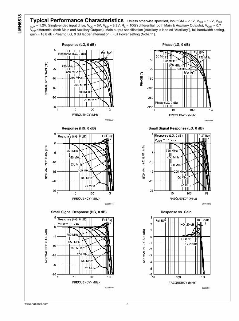
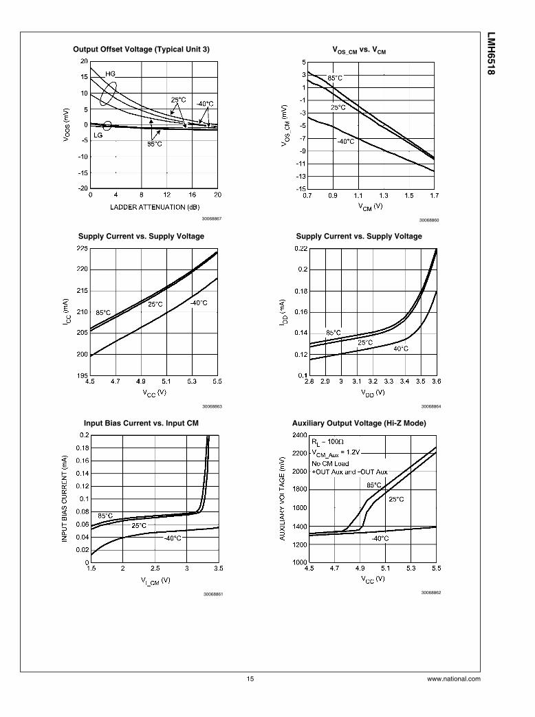
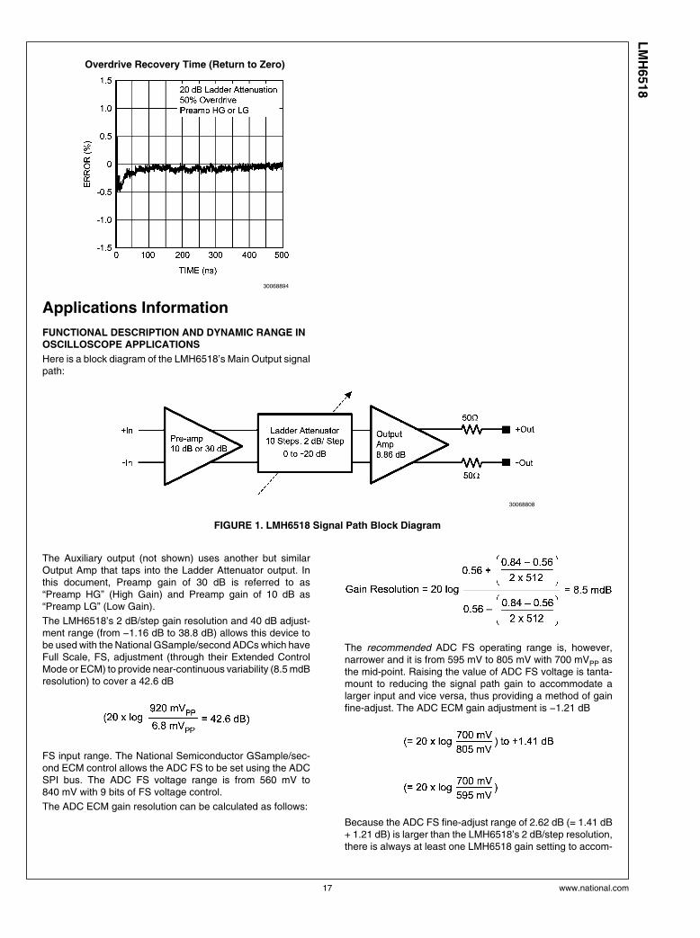
Typical Performance Characteristics Unless otherwise specified, Input CM = 2.5V, VCM = 1.2V, VCM
AUX = 1.2V, Single-ended input drive, VCC = 5V, VDD = 3.3V, RL = 100Ω differential (both Main & Auxiliary Outputs), VOUT = 0.7
VPP differential (both Main and Auxiliary Outputs), Main output specification (Auxiliary is labeled “Auxiliary”), full bandwidth setting,
gain = 18.8 dB (Preamp LG, 0 dB ladder attenuation), Full Power setting (Note 11).
Response (LG, 0 dB)
30068842
Phase (LG, 0 dB)
30068843
Response (HG, 0 dB)
30068844
Small Signal Response (LG, 0 dB)
30068845
Small Signal Response (HG, 0 dB)
30068846
Response vs. Gain
30068851
www.national.com 8
LM
H6518

Phase vs. Gain
30068852
Response Over Temperature
30068856
Auxiliary Response Over Temperature
30068855
Main vs. Auxiliary Response
30068854
Response vs. Gain
30068847
Phase vs. Gain
30068848
9 www.national.com
LM
H6518

Response vs. Gain
30068849
Phase vs. Gain
30068850
Balance Error
30068853
Linear Phase Deviation and Group Delay
30068840
Noise vs. Ladder Attenuation
30068807
Noise vs. Ladder Attenuation
30068837
www.national.com 10
LM
H6518
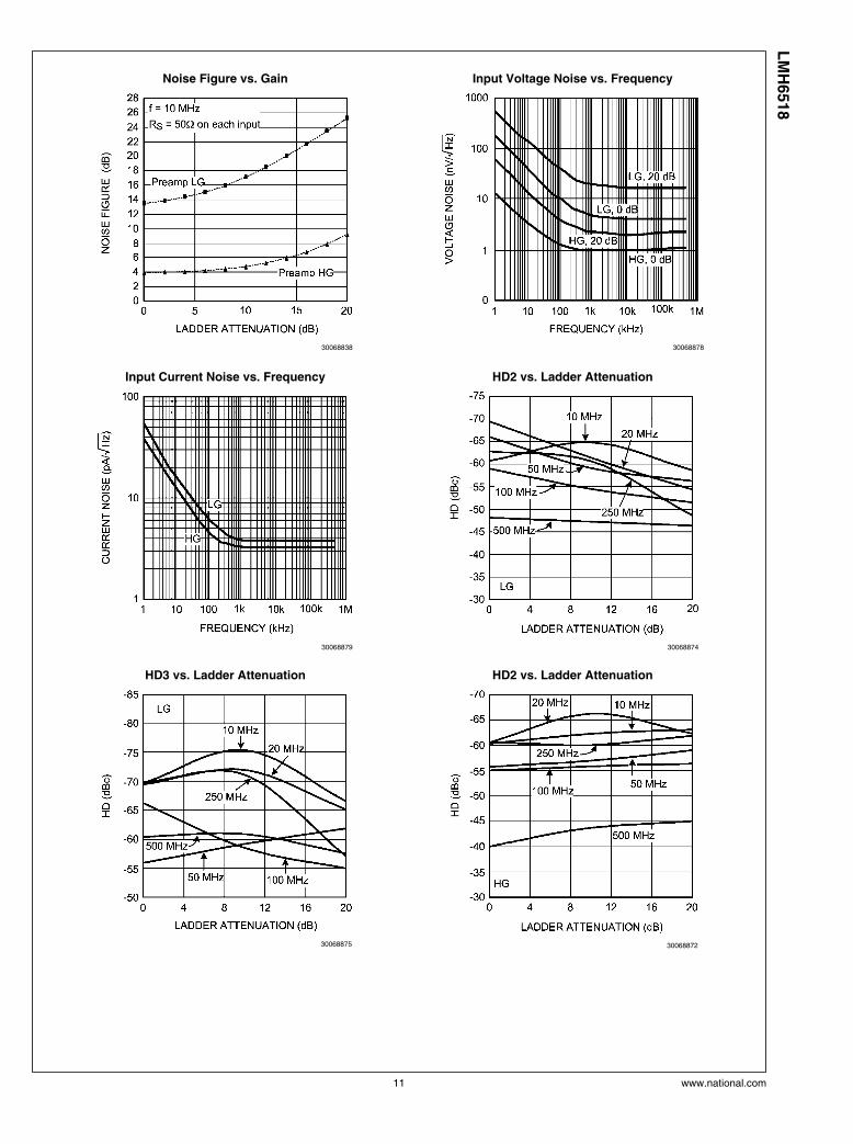
Noise Figure vs. Gain
30068838
Input Voltage Noise vs. Frequency
30068878
Input Current Noise vs. Frequency
30068879
HD2 vs. Ladder Attenuation
30068874
HD3 vs. Ladder Attenuation
30068875
HD2 vs. Ladder Attenuation
30068872
11 www.national.com
LM
H6518

HD3 vs. Ladder Attenuation
30068873
Main and Auxiliary Distortion Comparison
30068896
Main and Auxiliary Distortion Comparison
30068897
Distortion vs. Output Power
30068898
Gain vs. Ladder Attenuation
30068871
Gain Accuracy vs. Ladder Attenuation
30068869
www.national.com 12
LM
H6518
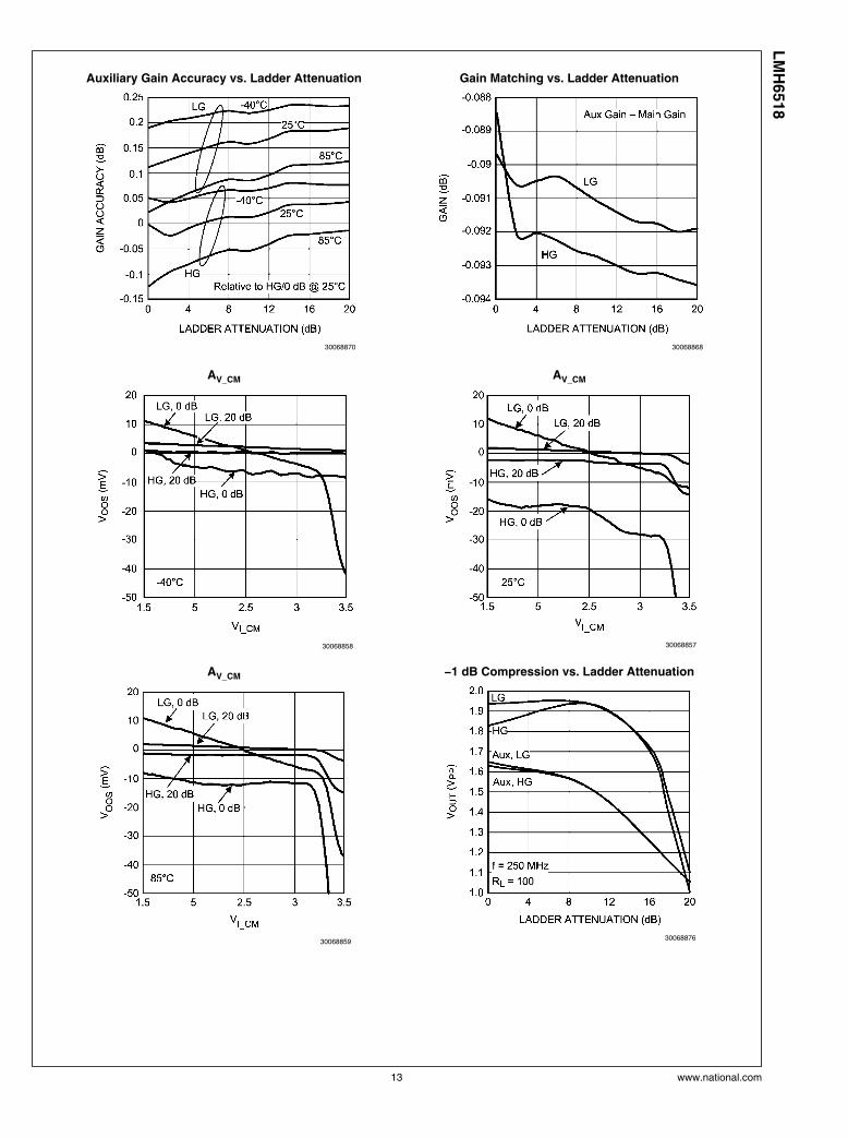
Auxiliary Gain Accuracy vs. Ladder Attenuation
30068870
Gain Matching vs. Ladder Attenuation
30068868
AV_CM
30068858
AV_CM
30068857
AV_CM
30068859
−1 dB Compression vs. Ladder Attenuation
30068876
13 www.national.com
LM
H6518

Step Response
30068889
Step Response
30068890
Step Response
30068891
Step Response
30068892
Output Offset Voltage (Typical Unit 1)
30068865
Output Offset Voltage (Typical Unit 2)
30068866
www.national.com 14
LM
H6518
Output Offset Voltage (Typical Unit 3)
30068867
VOS_CM vs. VCM
30068860
Supply Current vs. Supply Voltage
30068863
Supply Current vs. Supply Voltage
30068864
Input Bias Current vs. Input CM
30068861
Auxiliary Output Voltage (Hi-Z Mode)
30068862
15 www.national.com
LM
H6518

Filter BW vs. Gain
30068895
Output vs. Input
30068880
Output vs. Input
30068881
Output vs. Input
30068882
Output vs. Input
30068883
Overdrive Recovery Time (Return to Zero)
30068893
www.national.com 16
LM
H6518
Overdrive Recovery Time (Return to Zero)
30068894
Applications Information
FUNCTIONAL DESCRIPTION AND DYNAMIC RANGE INOSCILLOSCOPE APPLICATIONS
Here is a block diagram of the LMH6518’s Main Output signalpath:
30068808
FIGURE 1. LMH6518 Signal Path Block Diagram
The Auxiliary output (not shown) uses another but similarOutput Amp that taps into the Ladder Attenuator output. Inthis document, Preamp gain of 30 dB is referred to as“Preamp HG” (High Gain) and Preamp gain of 10 dB as“Preamp LG” (Low Gain).
The LMH6518’s 2 dB/step gain resolution and 40 dB adjust-ment range (from −1.16 dB to 38.8 dB) allows this device tobe used with the National GSample/second ADCs which haveFull Scale, FS, adjustment (through their Extended ControlMode or ECM) to provide near-continuous variability (8.5 mdBresolution) to cover a 42.6 dB
FS input range. The National Semiconductor GSample/sec-ond ECM control allows the ADC FS to be set using the ADCSPI bus. The ADC FS voltage range is from 560 mV to840 mV with 9 bits of FS voltage control.
The ADC ECM gain resolution can be calculated as follows:
The recommended ADC FS operating range is, however,narrower and it is from 595 mV to 805 mV with 700 mVPP asthe mid-point. Raising the value of ADC FS voltage is tanta-mount to reducing the signal path gain to accommodate alarger input and vice versa, thus providing a method of gainfine-adjust. The ADC ECM gain adjustment is −1.21 dB
Because the ADC FS fine-adjust range of 2.62 dB (= 1.41 dB+ 1.21 dB) is larger than the LMH6518’s 2 dB/step resolution,there is always at least one LMH6518 gain setting to accom-
17 www.national.com
LM
H6518

modate any FS signal from 6.8 mVPP to 920 mVPP, at theLMH6518 input, with 0.62 dB (= 2.62-2) overlap.
Assuming a nominal 0.7VPP output, the LMH6518’s minimumFS input swing is limited by the maximum signal path gainpossible and vice versa:
(or 8 mVPP with no ADC fine adjust)
(or 800 mVPP with no ADC FS adjust)
To accommodate a higher FS input, an additional attenuatoris needed before the LMH6518. This front-end attenuator isshown in the Figure 6 block diagram with its details shown inFigure 15. The highest minimum attenuation level is deter-mined by the largest FS input signal (FSmax):
So, to accommodate 80 VPP, 40 dB minimum attenuation isneeded before the LMH6518.
In a typical oscilloscope application, the voltage range en-countered is from 1 mV/DIV to 10 V/DIV with 8 vertical divi-sions visible on the screen. One of the primary concerns in adigital oscilloscope is SNR which translates to display tracewidth/ thickness. Typically, oscilloscope manufacturers needthe noise level to be low enough so that the “no-input” visibletrace width is less than 1% of FS. Experience has shown thatthis corresponds to a minimum SNR of 52 dB.
The factors that influence SNR are:
• Scope front end noise (Front-end attenuator + scopeprobe Hi-Z buffer which is discussed later in this documentand shown in Figure 6)
• LMH6518
• ADC
LMH6518 related SNR factors are:
• Bandwidth
• Preamp used (Preamp High Gain or Low Gain)
• Ladder Attenuation
• Signal level
SNR increases with the inverse square root of the bandwidth.So, reducing bandwidth from 450 MHz to 200 MHz, for ex-ample, improves SNR by 3.5 dB
The other factors listed above, preamp and ladder attenua-tion, depend on the signal level and also impact SNR. Thecombined effect of these factors is summarized in Figure 2where SNR is plotted as a function of the LMH6518 FS inputvoltage (assuming scope bandwidth of 200 MHz) and not in-cluding the ADC and the front end noise:
30068815
FIGURE 2. LMH6518 SNR & Ladder Attenuation used vs.Input
As can be seen from Figure 2, SNR of at least 52 dB is main-tained for FS inputs above 24 mVPP (3 mV/DIV on a scope)assuming the LMH6518’s internal 200 MHz filter is enabled.Most oscilloscope manufacturers relax the SNR specifica-tions to 40 dB for the highest gain (lowest scope voltagesetting) . From Figure 2, LMH6518’s minimum SNR is 43.5dB, thereby meeting the relaxed SNR specification for thelower range of scope front panel voltages.
In Figure 2, the step-change in SNR near Input FS of90 mVPP is the transition point from Preamp LG to PreampHG with a subsequent 3 dB difference due to the Preamp HG/20 dB ladder attenuation’s lower output noise compared toPreamp LG/ 2 dB ladder attenuation’s noise. Judicious choiceof front end attenuators can ensure that the 52 dB SNR spec-ification is maintained for scope FS inputs ≥ 24 mVPP byconfining the LMH6518 gain range to the lower 30.5 dB
from the total range of 40 dB (= 38.8 - (−1.16)) possible.
Here is an example:
To cover the range of 1 mV/DIV to 10 V/DIV (80 dB range),here is a configuration which affords good SNR:
www.national.com 18
LM
H6518
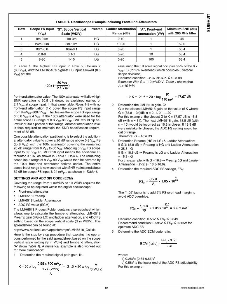
TABLE 1. Oscilloscope Example Including Front-End Attenuators
Row Scope FS Input
(VPP)“S”, Scope Vertical
Scale (V/DIV)
Preamp Ladder Attenuation
Range (dB)“A”, Front-end
attenuation (V/V)
Minimum SNR (dB)
with 200 MHz filter
1 8m-24m 1m-3m HG 0-10 1 44
2 24m-80m 3m-10m HG 10-20 1 52.0
3 80m-0.8 10m-0.1 LG 0-20 1 53.4
4 0.8-8 0.1-1 LG 0-20 10 53.4
5 8-80 1-10 LG 0-20 100 53.4
In Table 1, the highest FS input in Row 5, Column 2(80 VPP), and the LMH6518’s highest FS input allowed (0.8VPP) set the
front-end attenuator value. The 100x attenuator will allow highSNR operation to 30.5 dB down, as explained earlier, or2.4 VPP at scope input. In that same table, Rows 1-3 with nofront-end attenuation (1x) cover the scope FS input rangefrom 8 mVPP-800 mVPP. That leaves the scope FS input rangeof 0.8 VPP-2.4 VPP. If the 100x attenuator were used for theentire scope FS range of 0.8 VPP-80 VPP, SNR would dip be-low 52 dB for a portion of that range. Another attenuation levelis thus required to maintain the SNR specification require-ment of 52 dB.
One possible attenuation partitioning is to select the addition-al attenuator value to cover a 20 dB range above 0.8 VPP FS(to 8 VPP) with the 100x attenuator covering the remaining20 dB range from 8 VPP to 80 VPP. Mapping 8 VPP FS scopeinput to 0.8 VPP at LMH6518 input means the additional at-tenuator is 10x, as shown in Table 1, Row 4. The remainingscope input range of 8 VPP-80 VPP would then be covered bythe 100x front-end attenuator derived earlier. The entirescope input range is now covered with SNR maintained about52 dB for scope FS input ≥ 24 mVPP, as shown in Table 1.
SETTINGS AND ADC SPI CODE (ECM)
Covering the range from 1 mV/DIV to 10 V/DIV requires thefollowing to be adjusted within the digital oscilloscope:
• Front-end attenuator
• LMH6518 Preamp
• LMH6518 Ladder Attenuation
• ADC FS value (ECM)
The LMH6518 Product Folder contains a spreadsheet whichallows one to calculate the front-end attenuator, LMH6518Preamp gain (HG or LG) and ladder attenuation, and ADC FSsetting based on the scope vertical scale (S in V/DIV). Thisspreadsheet can be found at:
http://www.national.com/appinfo/amps/LMH6518_Cal.xls
Here is the step by step procedure that explains the opera-tions performed by the said spreadsheet based on the scopevertical scale setting (S in V/div) and front-end attenuation“A” (from Table 1). A numerical example is also worked outfor more clarification:
1. Determine the required signal path gain, K:
(assuming the full scale signal occupies 95% of the 0.7VPP FS (for 5% overhead) which occupies 8 verticalscope divisions).Required condition: −2.37 dB ≤ K ≤ 40.3 dBExample: With S = 110 mV/DIV, Table 1 shows thatA = 10 V/V:
2. Determine the LMH6518 gain, G:G is the closest LMH6518 gain, to the value of K where:G = (38.8 – 2n)dB; n = 0, 1, 2, …, 20For this example, the closest G to K = 17.57 dB is 16.8dB (with n = 11). The next LMH6518 gain, 18.8 dB (withn = 10) would be incorrect as 16.8 is closer. If 18.8 dBwere mistakenly chosen, the ADC FS setting would beout of range.Therefore: G = 16.8 dB
3. Determine Preamp (HG or LG) & Ladder Attenuation:If G ≥ 18.8 dB → Preamp is HG and Ladder Attenuation= 38.8 - GIf G < 18.8 dB → Preamp is LG and Ladder Attenuation= 18.8 - GFor this example, with G = 16.8 → Preamp LG and LadderAttenuation = 2 dB (= 18.8-16.8).
4. Determine the required ADC FS voltage, FSE:
The “1.05” factor is to add 5% FS overhead margin toavoid ADC overdrive.
Required condition: 0.56V ≤ FSE ≤ 0.84VRecommend condition: 0.595V ≤ FSE ≤ 0.805V foroptimum ADC FS
5. Determine the ADC ECM code ratio:
where: a) 0.28V= (0.84-0.56)V b) 0.56V is the lower end of the ADC FS adjustabilityFor this example:
19 www.national.com
LM
H6518
Required condition: 0 ≤ ECM (ratio) ≤ 1
6. Determine the ECM binary code to be sent on ADC SPIbus:Convert the ECM value represented by the ratiocalculated above, to binary:ECM (binary) = DEC2BINECM(ratio)* 511, 9
where “DEC2BIN” is a spreadsheet function whichconverts the decimal ECM ratio, from step 5 above,multiplied by 511 distinct levels, into binary 9 bits.Note: The Web based spreadsheet computes ECM without the use of
“DEC2BIN” function to ease usage by all spreadsheet userswho may not have this function installed.
For this example: ECM (binary) = DEC2BIN(0.283*511,9) = 010010000. This would be the number to be sent tothe ADC on the SPI bus to program the ADC to the properFS voltage.
INPUT/OUTPUT CONSIDERATIONSThe LMH6518’s ideal Input/Output Conditions, considered in-dividually, are listed below:
TABLE 2. LMH6518's Ideal Input/Output Conditions
Impedance from
each input to
ground (Ω)
Common Mode
Input (V)
Differential Input
(VPP)
Load Impedance
(Ω)Differential Output
(V)
Common Mode
Output (V)
≤50 1.5 to 3.1 <0.8 100 (differential)/ 50
(single ended)
<0.77 0.95-1.45
In addition to the individual conditions listed in Table 2, theInput/Output terminal conditions should match differentially(i.e. +IN to −IN and +OUT to −OUT), as well, for best perfor-mance.
The input is differential but can be driven single-ended as longas the conditions of Table 2 are met and there is good match-ing between the driven and the undriven inputs from DC tothe highest frequency of interest. If not, there could be a set-tling time impact among other possible performance degra-dations. The datasheet specifications are with single-endedinput, unless specified. Here is the recommended bench-testschematic to drive one input and to bias the other input withgood matching in mind:
30068824
FIGURE 3. Recommended Single-Ended Bench-TestInput Drive from 50Ω Source
With the schematic of Figure 3, each LMH6518 input sees25Ω to ground at the higher frequencies when the capacitorslook like shorts. This impedance increases to 125Ω at DC forboth inputs, thereby preserving the required matching at anyfrequency. This configuration, using properly selected R’sand C’s, allows four times less biasing power dissipation thanwhen the undriven input is biased with an effective 25Ω fromthe LMH6518 input to ground.
It is possible to drive the LMH6518 input from a ground ref-erenced 50Ω source by providing level shift circuitry on thedriven input. Figure 4 shows a circuit where ½ the input signalreaches the LMH6518 input while the negative supply voltage
(VEE) ensures that the 50Ω source at J1 does not experienceany biasing current while providing 50Ω termination to thesource. The driven input (+IN) is biased to 2.5V (VCC/2):
30068825
FIGURE 4. LMH6518 Driven by a Ground ReferencedSource
In the schematic of Figure 4, the equivalent impedance fromeach LMH6518 input to ground is around 38Ω. Thisconfiguration’s power consumption of ∼0.5W (in R1 - R5) ishigher than that of Figure 3 because of additional power dis-sipated to perform the level shifting. Additional 50Ω attenua-tors can be placed between J1 and R2/R3 junction in Figure4 in order to accommodate higher input voltages.
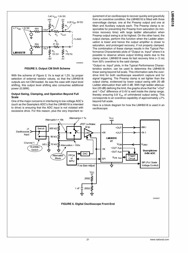
It is also possible to shift the LMH6518 output common modelevel using a level shift approach similar to that of Figure 4.The circuit in Figure 5 shows an implementation where theLMH6518’s nominal 1.2V CM output, set by a 1.2V on VCMinput from the Gsample/s ADC, is shifted lower for proper in-terface to different ADC's which require VCM = 0V and havehigh input impedance:
www.national.com 20
LM
H6518
30068826
FIGURE 5. Output CM Shift Scheme
With the scheme of Figure 5, Vx is kept at 1.2V, by properselection of external resistor values, so that the LMH6518outputs are not CM-loaded. As was the case with input levelshifting, this output level shifting also consumes additionalpower (0.58W).
Output Swing, Clamping, and Operation Beyond FullScale
One of the major concerns in interfacing to low voltage ADC’s(such as the Gsample/s ADC’s that the LMH6518 is intendedto drive) is ensuring that the ADC input is not violated withexcessive drive. For this reason, plus the very important re-
quirement of an oscilloscope to recover quickly and gracefullyfrom an overdrive condition, the LMH6518 is fitted with threeovervoltage clamps; one at the Preamp output and one atMain and Auxiliary outputs each. The Preamp clamp is re-sponsible for preventing the Preamp from saturation (to min-imize recovery time) with large ladder attenuation whenPreamp output swing is at its highest. On the other hand, theoutput clamps, perform this function when the Ladder atten-uation is lower and hence the output amplifier is closer tosaturation, and prolonged recovery, if not properly clamped.The combination of these clamps results in the Typical Per-formance Characteristic plots of “Output vs. Input” where it ispossible to observe where output limiting starts due to theclamp action. LMH6518 owes its fast recovery time (< 5 ns)from 50% overdrive to the said clamps.
“Output vs. Input” plots, in the Typical Performance Charac-teristics section, can be used to determine the LMH6518linear swing beyond full scale. This information sets the over-drive limit for both oscilloscope waveform capture and forsignal triggering. The Preamp clamp is set tighter than theoutput clamp, evidenced by lower output swing with 20 dBLadder attenuation than with 0 dB. With high ladder attenua-tion (20 dB) defining the limit, the graphs show that the “+Out”and “−Out” difference of 0.4V is well inside the clamp range,thereby ensuring 0.8 VPP of unhindered output swing. Thiscorresponds to an overdrive capability of approximately ±7%beyond full scale.
Here is a block diagram for how the LMH6518 is used in anoscilloscope:
30068827
FIGURE 6. Digital Oscilloscope Front-End
21 www.national.com
LM
H6518
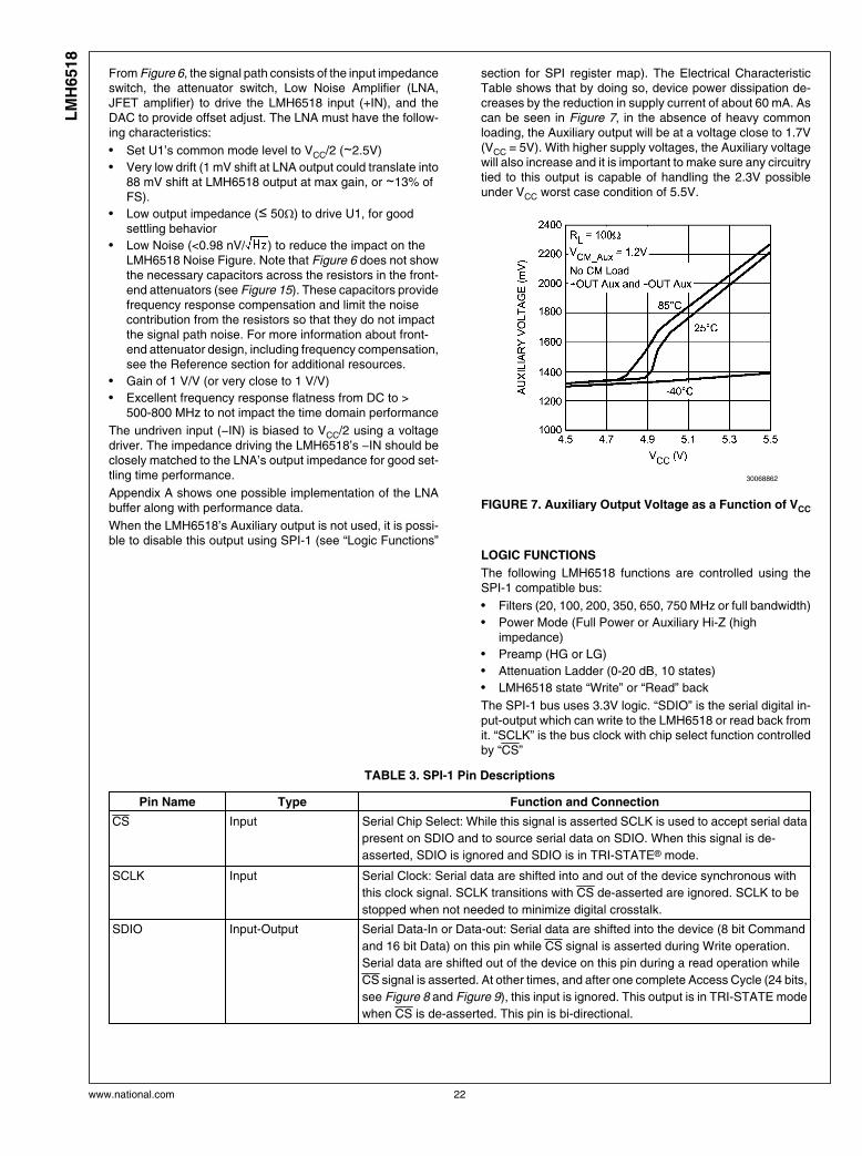
From Figure 6, the signal path consists of the input impedanceswitch, the attenuator switch, Low Noise Amplifier (LNA,JFET amplifier) to drive the LMH6518 input (+IN), and theDAC to provide offset adjust. The LNA must have the follow-ing characteristics:
• Set U1’s common mode level to VCC/2 (∼2.5V)
• Very low drift (1 mV shift at LNA output could translate into88 mV shift at LMH6518 output at max gain, or ∼13% ofFS).
• Low output impedance (≤ 50Ω) to drive U1, for goodsettling behavior
• Low Noise (<0.98 nV/ ) to reduce the impact on theLMH6518 Noise Figure. Note that Figure 6 does not showthe necessary capacitors across the resistors in the front-end attenuators (see Figure 15). These capacitors providefrequency response compensation and limit the noisecontribution from the resistors so that they do not impactthe signal path noise. For more information about front-end attenuator design, including frequency compensation,see the Reference section for additional resources.
• Gain of 1 V/V (or very close to 1 V/V)
• Excellent frequency response flatness from DC to >500-800 MHz to not impact the time domain performance
The undriven input (−IN) is biased to VCC/2 using a voltagedriver. The impedance driving the LMH6518’s −IN should beclosely matched to the LNA’s output impedance for good set-tling time performance.
Appendix A shows one possible implementation of the LNAbuffer along with performance data.
When the LMH6518’s Auxiliary output is not used, it is possi-ble to disable this output using SPI-1 (see “Logic Functions”
section for SPI register map). The Electrical CharacteristicTable shows that by doing so, device power dissipation de-creases by the reduction in supply current of about 60 mA. Ascan be seen in Figure 7, in the absence of heavy commonloading, the Auxiliary output will be at a voltage close to 1.7V(VCC = 5V). With higher supply voltages, the Auxiliary voltagewill also increase and it is important to make sure any circuitrytied to this output is capable of handling the 2.3V possibleunder VCC worst case condition of 5.5V.
30068862
FIGURE 7. Auxiliary Output Voltage as a Function of VCC
LOGIC FUNCTIONS
The following LMH6518 functions are controlled using theSPI-1 compatible bus:
• Filters (20, 100, 200, 350, 650, 750 MHz or full bandwidth)
• Power Mode (Full Power or Auxiliary Hi-Z (highimpedance)
• Preamp (HG or LG)
• Attenuation Ladder (0-20 dB, 10 states)
• LMH6518 state “Write” or “Read” back
The SPI-1 bus uses 3.3V logic. “SDIO” is the serial digital in-put-output which can write to the LMH6518 or read back fromit. “SCLK” is the bus clock with chip select function controlledby “CS”
TABLE 3. SPI-1 Pin Descriptions
Pin Name Type Function and Connection
CS Input Serial Chip Select: While this signal is asserted SCLK is used to accept serial data
present on SDIO and to source serial data on SDIO. When this signal is de-
asserted, SDIO is ignored and SDIO is in TRI-STATE® mode.
SCLK Input Serial Clock: Serial data are shifted into and out of the device synchronous with
this clock signal. SCLK transitions with CS de-asserted are ignored. SCLK to be
stopped when not needed to minimize digital crosstalk.
SDIO Input-Output Serial Data-In or Data-out: Serial data are shifted into the device (8 bit Command
and 16 bit Data) on this pin while CS signal is asserted during Write operation.
Serial data are shifted out of the device on this pin during a read operation while
CS signal is asserted. At other times, and after one complete Access Cycle (24 bits,
see Figure 8 and Figure 9), this input is ignored. This output is in TRI-STATE mode
when CS is de-asserted. This pin is bi-directional.
www.national.com 22
LM
H6518
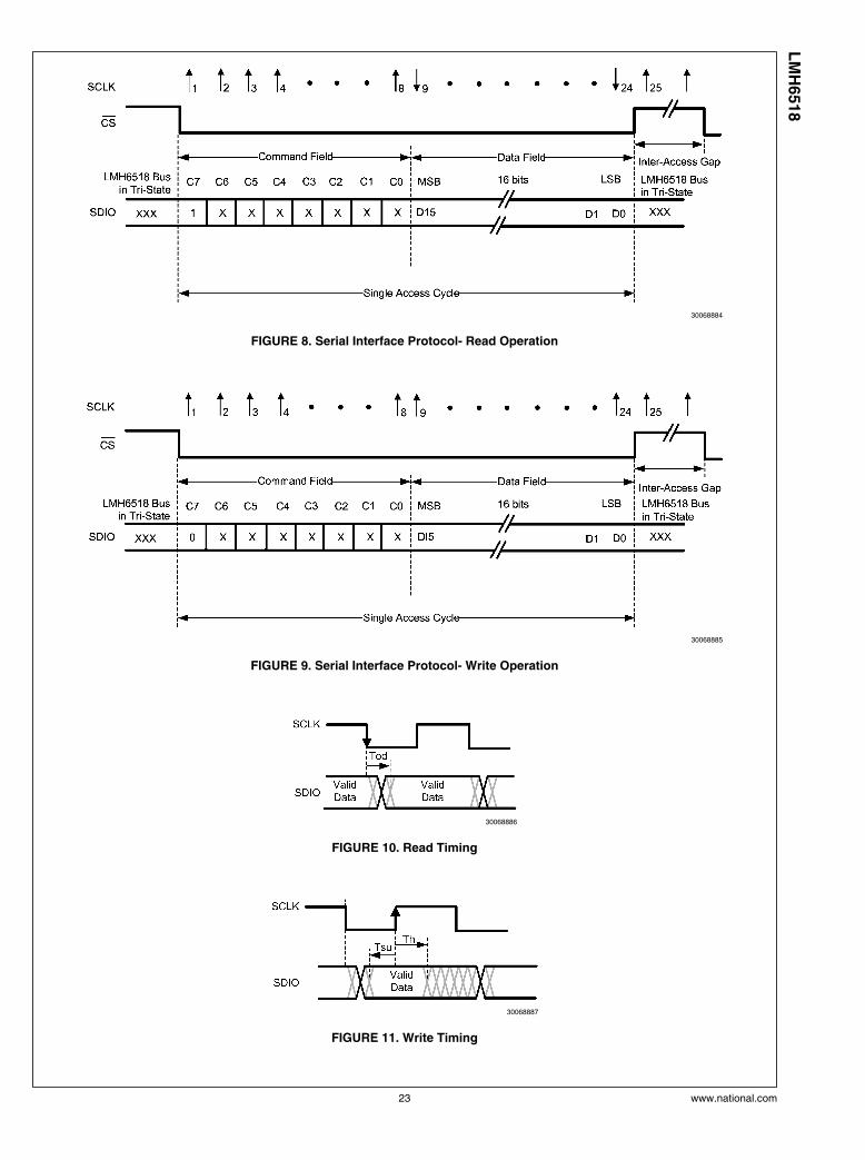
30068884
FIGURE 8. Serial Interface Protocol- Read Operation
30068885
FIGURE 9. Serial Interface Protocol- Write Operation
30068886
FIGURE 10. Read Timing
30068887
FIGURE 11. Write Timing
23 www.national.com
LM
H6518

TABLE 4. Data Field
Filter Pre-amp Ladder Attenuation
D15
(MSB)
D14 D13 D12 D11 D10 D9 D8 D7 D6 D5 D4 D3 D2 D1 D0
(LSB)
X 0 0 0 0 0=Full Power
1=Aux Hi-Z
0 See Table 6 0 0=LG
1=HG
See Table 7
Note: Bits D5, D9, D11-D14 must be “0”. Otherwise, device operation isundefined and specifications are not guaranteed.
TABLE 5. Default Power-On Reset Condition
Filter Pre-amp Ladder Attenuation
D15
(MSB)
D14 D13 D12 D11 D10 D9 D8 D7 D6 D5 D4 D3 D2 D1 D0
(LSB)
0 0 0 0 0 0 0 0 0 0 0 0 1 0 1 0
TABLE 6. Filer Selection Data Field
Filter Filter BW
D8 D7 D6 (MHz)
0 0 0 Full
0 0 1 20
0 1 0 100
0 1 1 200
1 0 0 350
1 0 1 650
1 1 0 750
1 1 1 Unallowed
Note: All filters are low pass single pole roll-off and operate on both Mainand Auxiliary outputs. These filters are intended as signal path band-width and/ or noise limiting.
TABLE 7. Ladder Attenuation Data Field
Ladder Attenuation Ladder Attenuation
(dB)
D3 D2 D1 D0
0 0 0 0 0
0 0 0 1 −2
0 0 1 0 −4
0 0 1 1 −6
0 1 0 0 −8
0 1 0 1 −10
0 1 1 0 −12
0 1 1 1 −14
1 0 0 0 −16
1 0 0 1 −18
1 0 1 0 −20
1 0 1 1 Unallowed
1 1 0 0 Unallowed
1 1 0 1 Unallowed
1 1 1 0 Unallowed
1 1 1 1 Unallowed
Note: An “Unallowed” SPI-1 state may result in undefined operation wheredevice behavior is not guaranteed.
www.national.com 24
LM
H6518
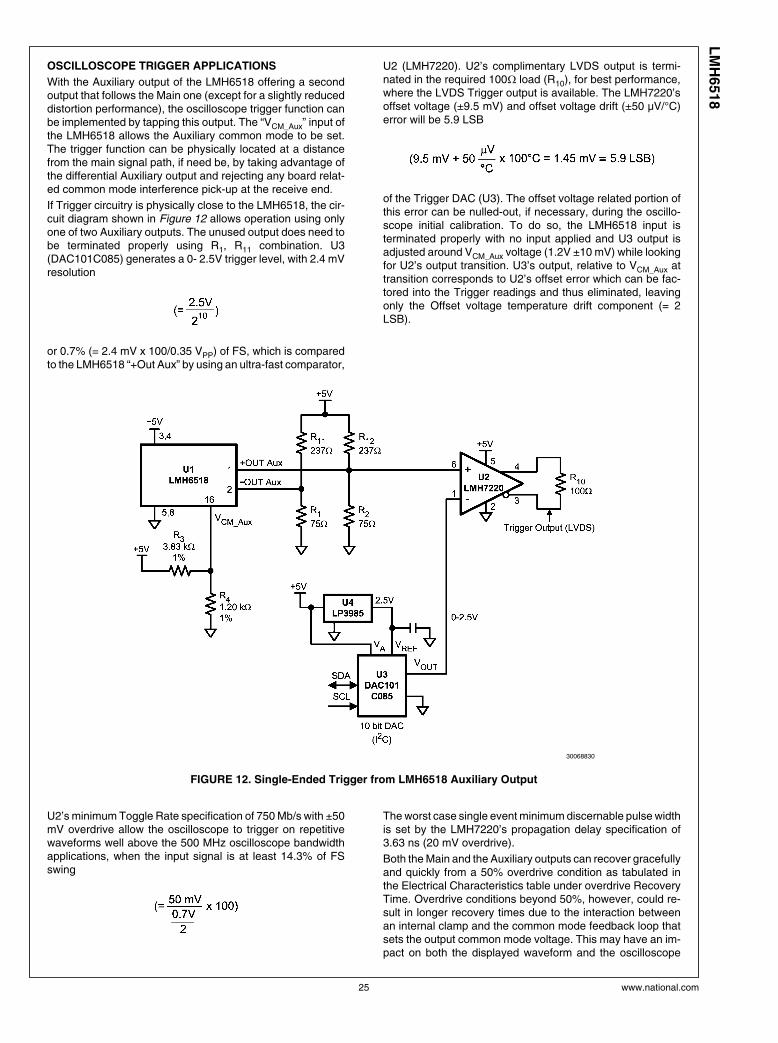
OSCILLOSCOPE TRIGGER APPLICATIONS
With the Auxiliary output of the LMH6518 offering a secondoutput that follows the Main one (except for a slightly reduceddistortion performance), the oscilloscope trigger function canbe implemented by tapping this output. The “VCM_Aux” input ofthe LMH6518 allows the Auxiliary common mode to be set.The trigger function can be physically located at a distancefrom the main signal path, if need be, by taking advantage ofthe differential Auxiliary output and rejecting any board relat-ed common mode interference pick-up at the receive end.
If Trigger circuitry is physically close to the LMH6518, the cir-cuit diagram shown in Figure 12 allows operation using onlyone of two Auxiliary outputs. The unused output does need tobe terminated properly using R1, R11 combination. U3(DAC101C085) generates a 0- 2.5V trigger level, with 2.4 mVresolution
or 0.7% (= 2.4 mV x 100/0.35 VPP) of FS, which is comparedto the LMH6518 “+Out Aux” by using an ultra-fast comparator,
U2 (LMH7220). U2’s complimentary LVDS output is termi-nated in the required 100Ω load (R10), for best performance,where the LVDS Trigger output is available. The LMH7220’soffset voltage (±9.5 mV) and offset voltage drift (±50 µV/°C)error will be 5.9 LSB
of the Trigger DAC (U3). The offset voltage related portion ofthis error can be nulled-out, if necessary, during the oscillo-scope initial calibration. To do so, the LMH6518 input isterminated properly with no input applied and U3 output isadjusted around VCM_Aux voltage (1.2V ±10 mV) while lookingfor U2’s output transition. U3’s output, relative to VCM_Aux attransition corresponds to U2’s offset error which can be fac-tored into the Trigger readings and thus eliminated, leavingonly the Offset voltage temperature drift component (= 2LSB).
30068830
FIGURE 12. Single-Ended Trigger from LMH6518 Auxiliary Output
U2’s minimum Toggle Rate specification of 750 Mb/s with ±50mV overdrive allow the oscilloscope to trigger on repetitivewaveforms well above the 500 MHz oscilloscope bandwidthapplications, when the input signal is at least 14.3% of FSswing
The worst case single event minimum discernable pulse widthis set by the LMH7220’s propagation delay specification of3.63 ns (20 mV overdrive).
Both the Main and the Auxiliary outputs can recover gracefullyand quickly from a 50% overdrive condition as tabulated inthe Electrical Characteristics table under overdrive RecoveryTime. Overdrive conditions beyond 50%, however, could re-sult in longer recovery times due to the interaction betweenan internal clamp and the common mode feedback loop thatsets the output common mode voltage. This may have an im-pact on both the displayed waveform and the oscilloscope
25 www.national.com
LM
H6518

Trigger. The result could be a loss of Trigger pulse and/orvisual distortion of the displayed waveform. To avoid this sce-nario, the oscilloscope should detect an excessive overdriveand go into trigger-loss mode. Done this way, the oscilloscopedisplay would show the last waveform that did not violate theoverdrive condition. Preferably there would be a visual indi-cator on the screen that alerts the user of the situation so that
he can correct the excessive condition to return to normaldisplay.
APPENDIX A
Here is the schematic drawing for a possible implementationof the LNA buffer shown in Figure 6:
30068835
FIGURE 13. JFET LNA Implementation
CIRCUIT OPERATION
This circuit uses an N-Channel JFET (J10) in Source-Follow-er configuration, to buffer the input signal, with J8 acting as aconstant current source. This buffer presents a fixed inputimpedance (1 MΩ||10 pF) with a gain close to 1 V/V.
The signal path is AC coupled through C7 with DC (and lowfrequency) at LMH6518 +IN maintained through the action ofU1. NPN transistor Q0 is an emitter follower which isolatesthe buffer from the load (LMH6518 input and board traces).
The undriven input of the LMH6518, −IN, is biased to 2.5V byR6, R9 voltage divider. The Lower ½ of U1 inverts this voltageand the upper ½ of U1 compares it to the combination of thedriven output level at LMH6518 +IN and the scaled version ofscope input at R14, R21 junction, and adjusts J10 Gate ac-cordingly to set the LMH6518 +IN. This control loop has afrequency response that covers DC to a few Hz, limited by theroll-off capacitor C3 and R15 combination (1st order approxi-mation). DC and low frequency gain is given by:
With the values in Figure 13 → R2 ≈ 452 kΩ: .
For a flat frequency response, the DC (low frequency) gainneeds to be lowered to match the less-than-1 V/V AC (highfrequency) path gain through the JFETs. This can be done byincreasing the value of R2.
By choosing the values of R15 and R11 so that
the frequency response at J10 Gate (and consequently theoutput) will remain flat when C7 starts to conduct. Offset cor-rection is done by varying the voltage at R4, using a DAC orequivalent as shown, in order to shift the LMH6518 +IN volt-age relative to −IN. The result is a circuit which shifts theground referenced scope input to 2.5V (VCC/2) CM with ad-justable offset and without any JFET or BJT related offsets.
Note that the front-end attenuator (not shown) lower leg re-sistance should be increased for proper divider-ratio to ac-count for the 1 MΩ shunt due to the series combination ofR21 and R14. For example, a 10:1 front-end attenuator couldbe formed by a series 900 kΩ and a shunt 111 kΩ for a scopeBNC input impedance of 1 MΩ (= 900K + (111K || 1M)).
www.national.com 26
LM
H6518

Table 8 lists other possible JFET candidates that fall in therange of speed (ft) and low noise needed:
TABLE 8. Suitable JFET Candidates Specifications
Company Part Number VP (V) Idss
(mA)
gm (mS) Input C
(pF)
noise *
(nV/RtHz)
Break
down (V)
Calculated ft
(MHz)
Interfet IF140 −2.2 10 5.5 2.3 4 −20 380
Interfet IF142 −2.2 10 5.5 2.3 4 −25 380
Interfet 2N5397/8 −2.5 13 8 5 2.5 −25 254
Interfet 2N5911/2 −2.5 13 8 5 2.5 254
Interfet J308/9/10 −2.3 21 17 5.8 −25 466
Philips BF513 -3 15 10 5 318
Fairchild MMBF5486 −4 14 7 4 2.5 −25 278
Vishay
Siliconix SST441 −3.5 13 6 3.5 4 −35 272
*Noise data at ∼ Idss/2
The LNA noise could degrade the scope’s SNR if it is com-parable to the input referred noise of the LMH6518. LNA noiseis influenced by the following operating conditions:
a) JFET equivalent input noise
b) BJT Base current
Reducing either “a” or “b” above, or both, reduces noise. Oneway to reduce “a” is to increase R8 (currently set to 0Ω). Thiswill reduce the noise impact of J8 but requires a JFET whichhas a higher Idss rating in order to maintain the operating cur-rent of J10 so that J10’s noise contribution is minimized.Reducing the BJT Base current can be accomplished with in-creasing R20 at the expenses of higher rise/fall times. A higherβ will also reduce the Base current (keep in mind that β andft at the operating Collector current is what matters).
Figure 14 shows the impact of the JFET buffer noise on SNR,compared to SNR in Figure 2, assuming either 3 nV/ or1.5 nV/ buffer noise for comparison:
30068834
FIGURE 14. LNA Buffer SNR Impact
ATTENUATOR DESIGN
Figure 15 shows a front-end attenuator designed to work withthe JFET LNA of Figure 13.
30068877
FIGURE 15. Front End Attenuator for Figure 13 JFET LNA
R_LNA” and “C_LNA” are the input impedance componentsof the JFET LNA. The 10:1 and 100:1 attenuators bottom re-sistors (R2 and R4) are adjusted higher to compensate for theLNA’s 1 MΩ input impedance, compared to the case where ahigh-input-impedance LNA is used. The two switches usedon the input and output of the attenuator block must be lowcapacitance, high isolation switches in order to reduce anyspeed or crosstalk impact. C1-C4 provide the proper frequen-cy response (and step response) by creating “zeros” thatflatten the response for wide-band operation. For the 10:1 at-tenuator, R1C1 = R2C2. The same applies to the 100:1 atten-uator. The shunt capacitors C1-C4 have a very important otherbenefit in that they roll-off the resistor thermal noise at a lowfrequency (low pass response, −3 dB down at ∼20 kHz)thereby eliminating any significant noise contribution from theattenuation resistors. Otherwise, the channel noise would bedominated by the attenuator resistor thermal noise. C2 andC6 trimmer capacitors can be adjusted to match the input ca-pacitance regardless of attenuator used.
REFERENCE
1. Wideband amplifiers by Peter Staric and Erik Margan, pub-lished by Springer in 2006. (Section 5.2).
27 www.national.com
LM
H6518

Physical Dimensions inches (millimeters) unless otherwise noted
16-Pin PackageNS Package Number SQA16A
www.national.com 28
LM
H6518

Notes
29 www.national.com
LM
H6518

NotesL
MH
6518 9
00 M
Hz,
Dig
itally C
on
tro
lled
, V
ari
ab
le G
ain
Am
plifi
er
For more National Semiconductor product information and proven design tools, visit the following Web sites at:
Products Design Support
Amplifiers www.national.com/amplifiers WEBENCH www.national.com/webench
Audio www.national.com/audio Analog University www.national.com/AU
Clock Conditioners www.national.com/timing App Notes www.national.com/appnotes
Data Converters www.national.com/adc Distributors www.national.com/contacts
Displays www.national.com/displays Green Compliance www.national.com/quality/green
Ethernet www.national.com/ethernet Packaging www.national.com/packaging
Interface www.national.com/interface Quality and Reliability www.national.com/quality
LVDS www.national.com/lvds Reference Designs www.national.com/refdesigns
Power Management www.national.com/power Feedback www.national.com/feedback
Switching Regulators www.national.com/switchers
LDOs www.national.com/ldo
LED Lighting www.national.com/led
PowerWise www.national.com/powerwise
Serial Digital Interface (SDI) www.national.com/sdi
Temperature Sensors www.national.com/tempsensors
Wireless (PLL/VCO) www.national.com/wireless
THE CONTENTS OF THIS DOCUMENT ARE PROVIDED IN CONNECTION WITH NATIONAL SEMICONDUCTOR CORPORATION(“NATIONAL”) PRODUCTS. NATIONAL MAKES NO REPRESENTATIONS OR WARRANTIES WITH RESPECT TO THE ACCURACYOR COMPLETENESS OF THE CONTENTS OF THIS PUBLICATION AND RESERVES THE RIGHT TO MAKE CHANGES TOSPECIFICATIONS AND PRODUCT DESCRIPTIONS AT ANY TIME WITHOUT NOTICE. NO LICENSE, WHETHER EXPRESS,IMPLIED, ARISING BY ESTOPPEL OR OTHERWISE, TO ANY INTELLECTUAL PROPERTY RIGHTS IS GRANTED BY THISDOCUMENT.
TESTING AND OTHER QUALITY CONTROLS ARE USED TO THE EXTENT NATIONAL DEEMS NECESSARY TO SUPPORTNATIONAL’S PRODUCT WARRANTY. EXCEPT WHERE MANDATED BY GOVERNMENT REQUIREMENTS, TESTING OF ALLPARAMETERS OF EACH PRODUCT IS NOT NECESSARILY PERFORMED. NATIONAL ASSUMES NO LIABILITY FORAPPLICATIONS ASSISTANCE OR BUYER PRODUCT DESIGN. BUYERS ARE RESPONSIBLE FOR THEIR PRODUCTS ANDAPPLICATIONS USING NATIONAL COMPONENTS. PRIOR TO USING OR DISTRIBUTING ANY PRODUCTS THAT INCLUDENATIONAL COMPONENTS, BUYERS SHOULD PROVIDE ADEQUATE DESIGN, TESTING AND OPERATING SAFEGUARDS.
EXCEPT AS PROVIDED IN NATIONAL’S TERMS AND CONDITIONS OF SALE FOR SUCH PRODUCTS, NATIONAL ASSUMES NOLIABILITY WHATSOEVER, AND NATIONAL DISCLAIMS ANY EXPRESS OR IMPLIED WARRANTY RELATING TO THE SALEAND/OR USE OF NATIONAL PRODUCTS INCLUDING LIABILITY OR WARRANTIES RELATING TO FITNESS FOR A PARTICULARPURPOSE, MERCHANTABILITY, OR INFRINGEMENT OF ANY PATENT, COPYRIGHT OR OTHER INTELLECTUAL PROPERTYRIGHT.
LIFE SUPPORT POLICY
NATIONAL’S PRODUCTS ARE NOT AUTHORIZED FOR USE AS CRITICAL COMPONENTS IN LIFE SUPPORT DEVICES ORSYSTEMS WITHOUT THE EXPRESS PRIOR WRITTEN APPROVAL OF THE CHIEF EXECUTIVE OFFICER AND GENERALCOUNSEL OF NATIONAL SEMICONDUCTOR CORPORATION. As used herein:
Life support devices or systems are devices which (a) are intended for surgical implant into the body, or (b) support or sustain life andwhose failure to perform when properly used in accordance with instructions for use provided in the labeling can be reasonably expectedto result in a significant injury to the user. A critical component is any component in a life support device or system whose failure to performcan be reasonably expected to cause the failure of the life support device or system or to affect its safety or effectiveness.
National Semiconductor and the National Semiconductor logo are registered trademarks of National Semiconductor Corporation. All otherbrand or product names may be trademarks or registered trademarks of their respective holders.
Copyright© 2008 National Semiconductor Corporation
For the most current product information visit us at www.national.com
National SemiconductorAmericas TechnicalSupport CenterEmail: [email protected]: 1-800-272-9959
National Semiconductor EuropeTechnical Support CenterEmail: [email protected] Tel: +49 (0) 180 5010 771English Tel: +44 (0) 870 850 4288
National Semiconductor AsiaPacific Technical Support CenterEmail: [email protected]
National Semiconductor JapanTechnical Support CenterEmail: [email protected]
www.national.com

IMPORTANT NOTICE
Texas Instruments Incorporated and its subsidiaries (TI) reserve the right to make corrections, modifications, enhancements, improvements,and other changes to its products and services at any time and to discontinue any product or service without notice. Customers shouldobtain the latest relevant information before placing orders and should verify that such information is current and complete. All products aresold subject to TI’s terms and conditions of sale supplied at the time of order acknowledgment.
TI warrants performance of its hardware products to the specifications applicable at the time of sale in accordance with TI’s standardwarranty. Testing and other quality control techniques are used to the extent TI deems necessary to support this warranty. Except wheremandated by government requirements, testing of all parameters of each product is not necessarily performed.
TI assumes no liability for applications assistance or customer product design. Customers are responsible for their products andapplications using TI components. To minimize the risks associated with customer products and applications, customers should provideadequate design and operating safeguards.
TI does not warrant or represent that any license, either express or implied, is granted under any TI patent right, copyright, mask work right,or other TI intellectual property right relating to any combination, machine, or process in which TI products or services are used. Informationpublished by TI regarding third-party products or services does not constitute a license from TI to use such products or services or awarranty or endorsement thereof. Use of such information may require a license from a third party under the patents or other intellectualproperty of the third party, or a license from TI under the patents or other intellectual property of TI.
Reproduction of TI information in TI data books or data sheets is permissible only if reproduction is without alteration and is accompaniedby all associated warranties, conditions, limitations, and notices. Reproduction of this information with alteration is an unfair and deceptivebusiness practice. TI is not responsible or liable for such altered documentation. Information of third parties may be subject to additionalrestrictions.
Resale of TI products or services with statements different from or beyond the parameters stated by TI for that product or service voids allexpress and any implied warranties for the associated TI product or service and is an unfair and deceptive business practice. TI is notresponsible or liable for any such statements.
TI products are not authorized for use in safety-critical applications (such as life support) where a failure of the TI product would reasonablybe expected to cause severe personal injury or death, unless officers of the parties have executed an agreement specifically governingsuch use. Buyers represent that they have all necessary expertise in the safety and regulatory ramifications of their applications, andacknowledge and agree that they are solely responsible for all legal, regulatory and safety-related requirements concerning their productsand any use of TI products in such safety-critical applications, notwithstanding any applications-related information or support that may beprovided by TI. Further, Buyers must fully indemnify TI and its representatives against any damages arising out of the use of TI products insuch safety-critical applications.
TI products are neither designed nor intended for use in military/aerospace applications or environments unless the TI products arespecifically designated by TI as military-grade or "enhanced plastic." Only products designated by TI as military-grade meet militaryspecifications. Buyers acknowledge and agree that any such use of TI products which TI has not designated as military-grade is solely atthe Buyer's risk, and that they are solely responsible for compliance with all legal and regulatory requirements in connection with such use.
TI products are neither designed nor intended for use in automotive applications or environments unless the specific TI products aredesignated by TI as compliant with ISO/TS 16949 requirements. Buyers acknowledge and agree that, if they use any non-designatedproducts in automotive applications, TI will not be responsible for any failure to meet such requirements.
Following are URLs where you can obtain information on other Texas Instruments products and application solutions:
Products Applications
Audio www.ti.com/audio Communications and Telecom www.ti.com/communications
Amplifiers amplifier.ti.com Computers and Peripherals www.ti.com/computers
Data Converters dataconverter.ti.com Consumer Electronics www.ti.com/consumer-apps
DLP® Products www.dlp.com Energy and Lighting www.ti.com/energy
DSP dsp.ti.com Industrial www.ti.com/industrial
Clocks and Timers www.ti.com/clocks Medical www.ti.com/medical
Interface interface.ti.com Security www.ti.com/security
Logic logic.ti.com Space, Avionics and Defense www.ti.com/space-avionics-defense
Power Mgmt power.ti.com Transportation and Automotive www.ti.com/automotive
Microcontrollers microcontroller.ti.com Video and Imaging www.ti.com/video
RFID www.ti-rfid.com
OMAP Mobile Processors www.ti.com/omap
Wireless Connectivity www.ti.com/wirelessconnectivity
TI E2E Community Home Page e2e.ti.com
Mailing Address: Texas Instruments, Post Office Box 655303, Dallas, Texas 75265Copyright © 2011, Texas Instruments Incorporated


