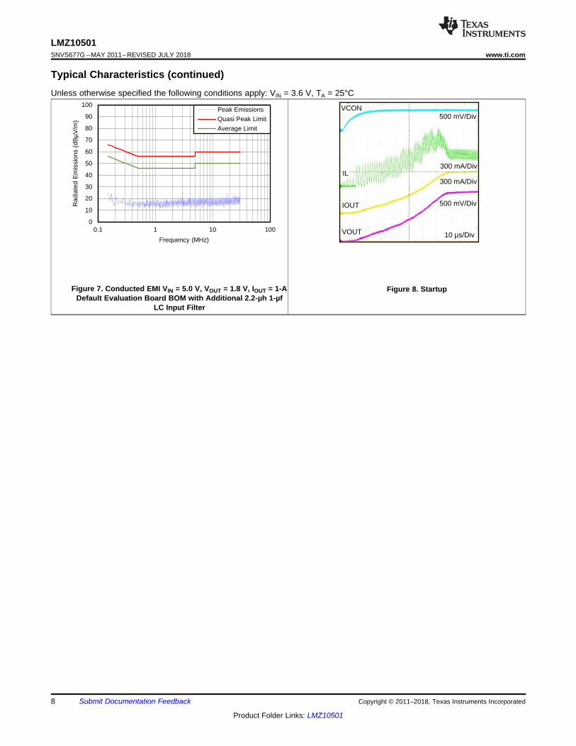
0 10 20 30 40 50 60 70 80 0 200 400 600 800 1000 Radiated Emissions (dBμV/m) Frequency (MHz) Evaluation Board EN 55022 Class B Limit EN 55022 Class A Limit C001 20 30 40 50 60 70 80 90 100 0.0 0.2 0.4 0.6 0.8 1.0 EFFICIENCY (%) LOAD CURRENT (A) VOUT=1.2V VOUT=1.8V VOUT=2.5V VOUT=3.3V C001 Product Folder Order Now Technical Documents Tools & Software Support & Community Reference Design An IMPORTANT NOTICE at the end of this data sheet addresses availability, warranty, changes, use in safety-critical applications, intellectual property matters and other important disclaimers. PRODUCTION DATA. LMZ10501 SNVS677G – MAY 2011 – REVISED JULY 2018 LMZ10501 1-A Nano Module With 5.5-V Maximum Input Voltage 1 1 Features 1• Output Current Up to 1 A • Input Voltage Range 2.7 V to 5.5 V • Output Voltage Range 0.6 V to 3.6 V • Efficiency up to 95% • Integrated Inductor • 8-Pin microSiP Footprint • –40°C to 125°C Junction Temperature Range • Adjustable Output Voltage • 2-MHz Fixed PWM Switching Frequency • Integrated Compensation • Soft-Start Function • Current Limit Protection • Thermal Shutdown Protection • Input Voltage UVLO for Power-Up, Power-Down, and Brownout Conditions • Only 5 External Components — Resistor Divider and 3 Ceramic Capacitors • Small Solution Size • Low Output Voltage Ripple • Easy Component Selection and Simple PCB Layout • High Efficiency Reduces System Heat Generation • Create a Custom Design Using the LMZ10501 With the WEBENCH ® Power Designer 2 Applications • Point of Load Conversions From 3.3-V and 5-V Rails • Space Constrained Applications • Low Output Noise Applications 3 Description The LMZ10501 nano module is an easy-to-use step- down DC-DC solution capable of driving up to 1-A load in space-constrained applications. Only an input capacitor, an output capacitor, a small V CON filter capacitor, and two resistors are required for basic operation. The nano module comes in an 8-pin μSIP footprint package with an inductor. Internal current limit based soft-start function, current overload protection, and thermal shutdown are also provided. Device Information (1) PART NUMBER PACKAGE BODY SIZE (NOM) LMZ10501 μSIP(8) 3.00 mm × 2.60 mm (1) For all available packages, see the orderable addendum at the end of the datasheet. Typical Efficiency at V IN = 3.6 V Radiated EMI (CISPR22) V IN = 5 V, V OUT = 1.8 V, I OUT =1A
Transcript
0
10
20
30
40
50
60
70
80
0 200 400 600 800 1000
Rad
iate
d E
mis
sion
s (d
Bµ
V/m
)
Frequency (MHz)
Evaluation Board
EN 55022 Class B Limit
EN 55022 Class A Limit
C001
20
30
40
50
60
70
80
90
100
0.0 0.2 0.4 0.6 0.8 1.0
EF
FIC
IEN
CY
(%
)
LOAD CURRENT (A)
VOUT=1.2VVOUT=1.8VVOUT=2.5VVOUT=3.3V
C001
Product
Folder
Order
Now
Technical
Documents
Tools &
Software
Support &Community
ReferenceDesign
An IMPORTANT NOTICE at the end of this data sheet addresses availability, warranty, changes, use in safety-critical applications,intellectual property matters and other important disclaimers. PRODUCTION DATA.
LMZ10501SNVS677G –MAY 2011–REVISED JULY 2018
LMZ10501 1-A Nano Module With 5.5-V Maximum Input Voltage
1
1 Features1• Output Current Up to 1 A• Input Voltage Range 2.7 V to 5.5 V• Output Voltage Range 0.6 V to 3.6 V• Efficiency up to 95%• Integrated Inductor• 8-Pin microSiP Footprint• –40°C to 125°C Junction Temperature Range• Adjustable Output Voltage• 2-MHz Fixed PWM Switching Frequency• Integrated Compensation• Soft-Start Function• Current Limit Protection• Thermal Shutdown Protection• Input Voltage UVLO for Power-Up, Power-Down,
and Brownout Conditions• Only 5 External Components — Resistor Divider
and 3 Ceramic Capacitors• Small Solution Size• Low Output Voltage Ripple• Easy Component Selection and Simple PCB
Layout• High Efficiency Reduces System Heat Generation• Create a Custom Design Using the LMZ10501
With the WEBENCH® Power Designer
2 Applications• Point of Load Conversions From 3.3-V and 5-V
Rails• Space Constrained Applications• Low Output Noise Applications
3 DescriptionThe LMZ10501 nano module is an easy-to-use step-down DC-DC solution capable of driving up to 1-Aload in space-constrained applications. Only an inputcapacitor, an output capacitor, a small VCON filtercapacitor, and two resistors are required for basicoperation. The nano module comes in an 8-pin µSIPfootprint package with an inductor. Internal currentlimit based soft-start function, current overloadprotection, and thermal shutdown are also provided.
Device Information(1)
PART NUMBER PACKAGE BODY SIZE (NOM)LMZ10501 µSIP(8) 3.00 mm × 2.60 mm
(1) For all available packages, see the orderable addendum atthe end of the datasheet.
Typical Efficiency at VIN = 3.6 V Radiated EMI (CISPR22)VIN = 5 V, VOUT = 1.8 V, IOUT = 1 A
9 Power Supply Recommendations ...................... 219.1 Voltage Range ........................................................ 219.2 Current Capability ................................................... 219.3 Input Connection .................................................... 21
11 Device and Documentation Support ................. 2411.1 Device Support...................................................... 2411.2 Documentation Support ........................................ 2411.3 Receiving Notification of Documentation Updates 2411.4 Community Resources.......................................... 2411.5 Trademarks ........................................................... 2411.6 Electrostatic Discharge Caution............................ 2411.7 Glossary ................................................................ 25
12 Mechanical, Packaging, and OrderableInformation ........................................................... 25
4 Revision HistoryNOTE: Page numbers for previous revisions may differ from page numbers in the current version.
Changes from Revision F (November 2014) to Revision G Page
• Editorial rebranding for SEO................................................................................................................................................... 1• Added links for Webench and top navigator icon for TI reference design ............................................................................ 1• Move storage temperature spec to Abs Max table ................................................................................................................ 4• Changed "Handling" to "ESD" Ratings .................................................................................................................................. 4• Added Device Support ......................................................................................................................................................... 24• Changed SIL package drawing to SIL0008G ...................................................................................................................... 25
Changes from Revision E (January 2014) to Revision F Page
• Added Pin Configuration and Functions section, Handling Rating table, Feature Description section, DeviceFunctional Modes, Application and Implementation section, Power Supply Recommendations section, Layoutsection, Device and Documentation Support section, and Mechanical, Packaging, and Orderable Informationsection ................................................................................................................................................................................... 1
Changes from Revision D (March 2013) to Revision E Page
• Added new package SIL0008A ............................................................................................................................................. 3
EN 1 I Enable Input. Set this digital input higher than 1.2 V for normal operation. For shutdown, setlow. Pin is internally pulled up to VIN and can be left floating for always-on operation.
VCON 2 IOutput voltage control pin. Connect to analog voltage from resisitve divider or DAC/controllerto set the VOUT voltage. VOUT = 2.5 x VCON. Connect a small (470pF) capacitor from this pinto SGND to provide noise filtering.
FB 3 I Feedback of the error amplifier. Connect directly to output capacitor to sense VOUT.SGND 4 I Ground for analog and control circuitry. Connect to PGND at a single point.
VOUT 5 O Output Voltage. Connected to one terminal of the integrated inductor. Connect output filtercapacitor between VOUT and PGND.
PGND 6 I Power ground for the power MOSFETs and gate-drive circuitry.
VIN 7 I Voltage supply input. Connect ceramic capacitor between VIN and PGND as close aspossible to these two pins. Typical capacitor values are between 4.7 µF and 22 µF.
VREF 8 O 2.35-V voltage reference output. Typically connected to VCON pin through a resistive dividerto set the output voltage.
PAD I The center pad underneath the SIL0008A package is internally tied to SGND. Connect thispad to the ground plane for improved thermal performance.
(1) Stresses beyond those listed under Absolute Maximum Ratings may cause permanent damage to the device. These are stress ratingsonly, which do not imply functional operation of the device at these or any other conditions beyond those indicated under RecommendedOperating Conditions. Exposure to absolute-maximum-rated conditions for extended periods may affect device reliability.
(2) If Military/Aerospace specified devices are required, contact the Texas Instruments Sales Office/ Distributors for availability andspecifications.
(3) Absolute Maximum Ratings are limits beyond which damage to the device may occur. Operating Ratings are conditions under whichoperation of the device is intended to be functional. For the Electrical Characteristics table for specifications and test conditions.
6 Specifications
6.1 Absolute Maximum Ratingsover operating free-air temperature range (unless otherwise noted) (1) (2) (3)
MIN MAX UNITVIN, VREF to SGND −0.2 +6.0 VPGND to SGND −0.2 +0.2 VEN, FB, VCON (SGND
−0.2)(VIN +0.2)w/6 max
V
VOUT (PGND−0.2)
(VIN +0.2)w/6 max
V
Junction temperature (TJ-MAX) −40 125 °CMaximum lead temperature 260 °CStorage temperature, Tstg –65 150 °C
(1) JEDEC document JEP155 states that 500-V HBM allows safe manufacturing with a standard ESD control process.(2) JEDEC document JEP157 states that 250-V CDM allows safe manufacturing with a standard ESD control process.
6.2 ESD RatingsVALUE UNIT
V(ESD) Electrostatic dischargeHuman-body model (HBM), per ANSI/ESDA/JEDEC JS-001 (1) ±1000
VCharged-device model (CDM), per JEDEC specification JESD22-C101 (2) ±250
6.3 Recommended Operating Conditionsover operating free-air temperature range (unless otherwise noted)
MIN MAX UNITInput voltage 2.7 5.5 VRecommended load current 0 1000 mAJunction temperature, TJ −40 125 °C
(1) For more information about traditional and new thermal metrics, see the Semiconductor and IC Package Thermal Metrics applicationreport.
(2) Junction-to-ambient thermal resistance (RθJA) is based on 4-layer board thermal measurements, performed under the conditions andguidelines set forth in the JEDEC standards JESD51-1 to JESD51-11. RθJA varies with PCB copper area, power dissipation, and airflow.
(1) Min and Max limits are 100% production tested at 25°C. Limits over the operating temperature range are specified through correlationusing Statistical Quality Control (SQC) methods. Limits are used to calculate the Average Outgoing Quality Level (AOQL).
(2) Typical numbers are at 25°C and represent the most likely parametric norm.(3) Shutdown current includes leakage current of the high side PFET.(4) Current limit is built-in, fixed, and not adjustable.
6.5 Electrical Characteristicsover operating free-air temperature range (unless otherwise noted). Typical values represent the most likely parametric normat TJ = 25°C, and are provided for reference purposes only. Unless otherwise stated the following conditions apply: VIN = 3.6V, VEN = 1.2 V. (1)
PARAMETER TEST CONDITIONS MIN (1) TYP (2) MAX (1) UNITSYSTEM PARAMETERS
VREF × GAIN Reference voltage × VCON toFB bain
VIN = VEN = 5.5V, VCON =1.44V 5.7575 5.875 5.9925 V
GAIN VCON to FB Gain VIN = 5.5V, VCON = 1.44V 2.4375 2.5 2.5750 V/VVINUVLO VIN rising threshold 2.24 2.41 2.64 VVINUVLO HYST VIN UVLO hysteresis 120 165 200 mVISHDN Shutdown supply current VIN = 3.6V, VEN = 0.5V (3) 11 18 µA
Iq DC bias current into VIN VIN = 5.5V, VCON = 1.6V,IOUT = 0A 6.5 9.5 mA
RDROPOUT VIN to VOUTresistance IOUT = 200 mA 305 575 mΩ
I LIM DC output current limit VCON = 1.72V (4) 1025 1350 mAFOSC Internal oscillator frequency 1.75 2.0 2.25 MHzVIH,ENABLE Enable logic HIGH voltage 1.2 VVIL,ENABLE Enable logic LOW voltage 0.5 VTSD Thermal shutdown Rising Threshold 150 °CTSD-HYST Thermal shutdown hysteresis 20 °CDMAX Maximum duty cycle 100%TON-MIN Minimum on-time 50 ns
θJASIL0008A Package ThermalResistance
20mm x 20mm board2 layers, 2 oz copper, 0.5W,no airlow
77
°C/W15mm x 15mm board2 layers, 2 oz copper, 0.5W,no airlow
88
10mm x 10mm board2 layers, 2 oz copper, 0.5W,no airlow
107
6.6 System CharacteristicsThe following specifications are ensured by design providing the component values in Figure 12 are used (CIN = COUT = 10µF, 6.3 V, 0603, TDK C1608X5R0J106K). These parameters are not ensured by production testing. Unless otherwise statedthe following conditions apply: TA = 25°C.
PARAMETER TEST CONDITIONS MIN TYP MAX UNIT
ΔVOUT/VOUT
Output voltage regulation over linevoltage and load current
VOUT = 0.6 VΔVIN = 2.7 V to 4.2 VΔIOUT = 0A to 1A
±1.75%
ΔVOUT/VOUT
Output voltage regulation over linevoltage and load current
VOUT = 1.5 VΔVIN = 2.7 V to 5.5 VΔIOUT = 0A to 1A
±0.92%
ΔVOUT/VOUT
Output voltage regulation over linevoltage and load current
VOUT = 3.6 VΔVIN = 4.0 V to 5.5 VΔIOUT = 0A to 1A
±0.38%
VREFTRISE
Rise time of reference voltage EN = Low to High, VIN = 4.2 VVOUT = 2.7 V, IOUT = 1A
System Characteristics (continued)The following specifications are ensured by design providing the component values in Figure 12 are used (CIN = COUT = 10µF, 6.3 V, 0603, TDK C1608X5R0J106K). These parameters are not ensured by production testing. Unless otherwise statedthe following conditions apply: TA = 25°C.
PARAMETER TEST CONDITIONS MIN TYP MAX UNIT
ηPeak efficiency VIN = 5.0 V, VOUT = 3.3 V
IOUT = 200 mA95%
Full load efficiency VIN = 5.0 V, VOUT = 3.6 VIOUT = 1000 mA
91%
VOUTRipple Output voltage ripple VIN = 5.0 V, VOUT = 1.8 V
IOUT = 1000 mA10 mV pk-pk
LineTransient Line transient response
VIN = 2.7 V to 5.5 V,TR = TF= 10 µs,VOUT = 1.8 V, IOUT = 1000 mA
30 mV pk-pk
LoadTransient Load transient response
VIN = 5.0 VTR = TF = 40 µs,VOUT = 1.8 VIOUT = 100 mA to 1000 mA
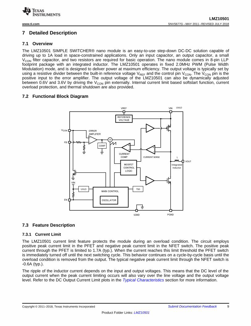
7.1 OverviewThe LMZ10501 SIMPLE SWITCHER® nano module is an easy-to-use step-down DC-DC solution capable ofdriving up to 1A load in space-constrained applications. Only an input capacitor, an output capacitor, a smallVCON filter capacitor, and two resistors are required for basic operation. The nano module comes in 8-pin LLPfootprint package with an integrated inductor. The LMZ10501 operates in fixed 2.0MHz PWM (Pulse WidthModulation) mode, and is designed to deliver power at maximum efficiency. The output voltage is typically set byusing a resistive divider between the built-in reference voltage VREF and the control pin VCON. The VCON pin is thepositive input to the error amplifier. The output voltage of the LMZ10501 can also be dynamically adjustedbetween 0.6V and 3.6V by driving the VCON pin externally. Internal current limit based softstart function, currentoverload protection, and thermal shutdown are also provided.
7.2 Functional Block Diagram
7.3 Feature Description
7.3.1 Current LimitThe LMZ10501 current limit feature protects the module during an overload condition. The circuit employspositive peak current limit in the PFET and negative peak current limit in the NFET switch. The positive peakcurrent through the PFET is limited to 1.7A (typ.). When the current reaches this limit threshold the PFET switchis immediately turned off until the next switching cycle. This behavior continues on a cycle-by-cycle basis until theoverload condition is removed from the output. The typical negative peak current limit through the NFET switch is-0.6A (typ.).
The ripple of the inductor current depends on the input and output voltages. This means that the DC level of theoutput current when the peak current limiting occurs will also vary over the line voltage and the output voltagelevel. Refer to the DC Output Current Limit plots in the Typical Characteristics section for more information.
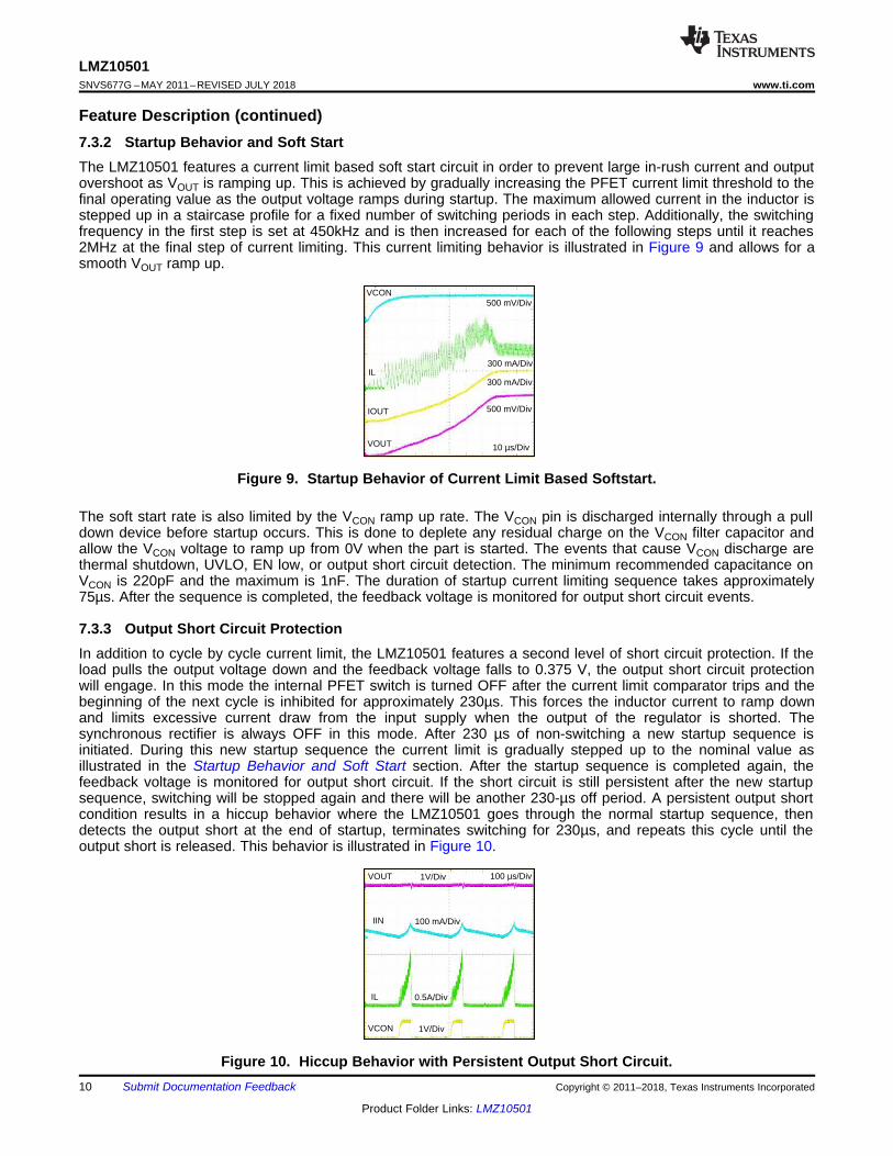
Feature Description (continued)7.3.2 Startup Behavior and Soft StartThe LMZ10501 features a current limit based soft start circuit in order to prevent large in-rush current and outputovershoot as VOUT is ramping up. This is achieved by gradually increasing the PFET current limit threshold to thefinal operating value as the output voltage ramps during startup. The maximum allowed current in the inductor isstepped up in a staircase profile for a fixed number of switching periods in each step. Additionally, the switchingfrequency in the first step is set at 450kHz and is then increased for each of the following steps until it reaches2MHz at the final step of current limiting. This current limiting behavior is illustrated in Figure 9 and allows for asmooth VOUT ramp up.
Figure 9. Startup Behavior of Current Limit Based Softstart.
The soft start rate is also limited by the VCON ramp up rate. The VCON pin is discharged internally through a pulldown device before startup occurs. This is done to deplete any residual charge on the VCON filter capacitor andallow the VCON voltage to ramp up from 0V when the part is started. The events that cause VCON discharge arethermal shutdown, UVLO, EN low, or output short circuit detection. The minimum recommended capacitance onVCON is 220pF and the maximum is 1nF. The duration of startup current limiting sequence takes approximately75µs. After the sequence is completed, the feedback voltage is monitored for output short circuit events.
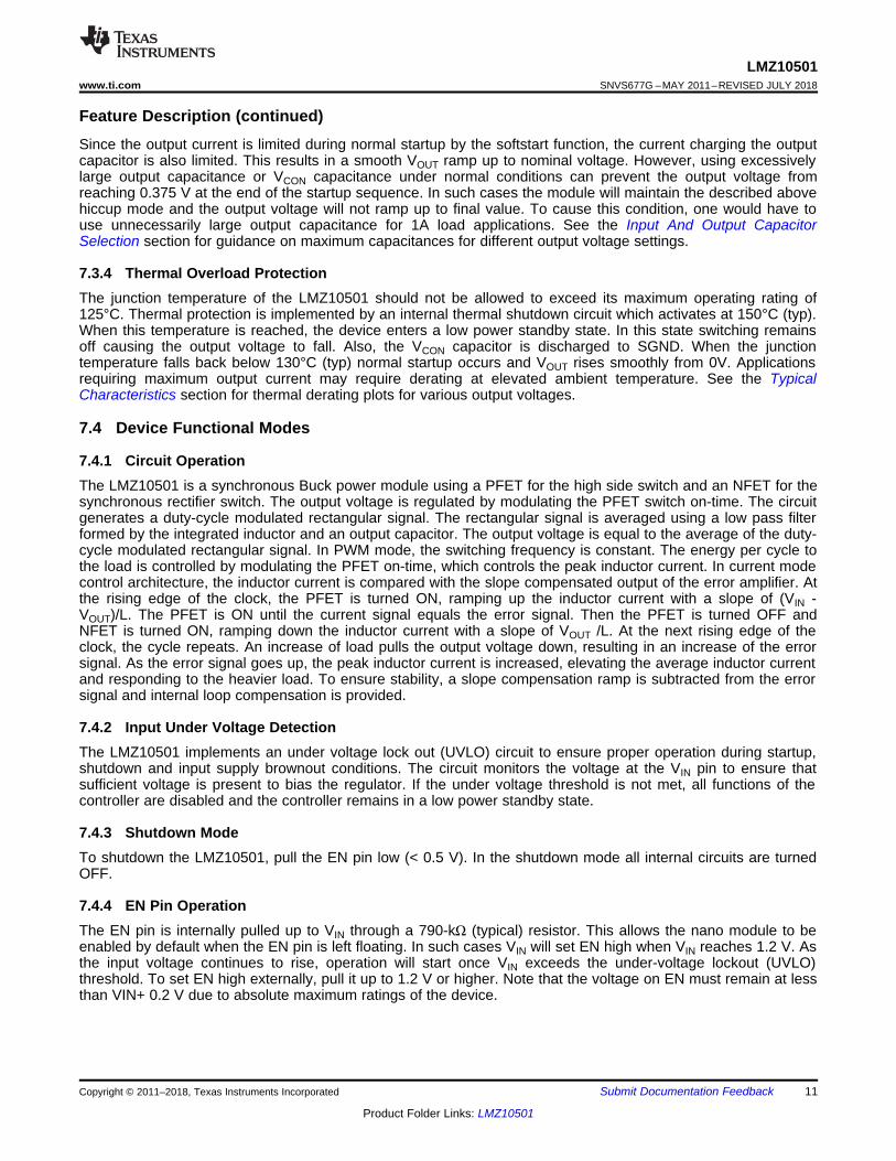
7.3.3 Output Short Circuit ProtectionIn addition to cycle by cycle current limit, the LMZ10501 features a second level of short circuit protection. If theload pulls the output voltage down and the feedback voltage falls to 0.375 V, the output short circuit protectionwill engage. In this mode the internal PFET switch is turned OFF after the current limit comparator trips and thebeginning of the next cycle is inhibited for approximately 230µs. This forces the inductor current to ramp downand limits excessive current draw from the input supply when the output of the regulator is shorted. Thesynchronous rectifier is always OFF in this mode. After 230 µs of non-switching a new startup sequence isinitiated. During this new startup sequence the current limit is gradually stepped up to the nominal value asillustrated in the Startup Behavior and Soft Start section. After the startup sequence is completed again, thefeedback voltage is monitored for output short circuit. If the short circuit is still persistent after the new startupsequence, switching will be stopped again and there will be another 230-µs off period. A persistent output shortcondition results in a hiccup behavior where the LMZ10501 goes through the normal startup sequence, thendetects the output short at the end of startup, terminates switching for 230µs, and repeats this cycle until theoutput short is released. This behavior is illustrated in Figure 10.
Figure 10. Hiccup Behavior with Persistent Output Short Circuit.
Feature Description (continued)Since the output current is limited during normal startup by the softstart function, the current charging the outputcapacitor is also limited. This results in a smooth VOUT ramp up to nominal voltage. However, using excessivelylarge output capacitance or VCON capacitance under normal conditions can prevent the output voltage fromreaching 0.375 V at the end of the startup sequence. In such cases the module will maintain the described abovehiccup mode and the output voltage will not ramp up to final value. To cause this condition, one would have touse unnecessarily large output capacitance for 1A load applications. See the Input And Output CapacitorSelection section for guidance on maximum capacitances for different output voltage settings.
7.3.4 Thermal Overload ProtectionThe junction temperature of the LMZ10501 should not be allowed to exceed its maximum operating rating of125°C. Thermal protection is implemented by an internal thermal shutdown circuit which activates at 150°C (typ).When this temperature is reached, the device enters a low power standby state. In this state switching remainsoff causing the output voltage to fall. Also, the VCON capacitor is discharged to SGND. When the junctiontemperature falls back below 130°C (typ) normal startup occurs and VOUT rises smoothly from 0V. Applicationsrequiring maximum output current may require derating at elevated ambient temperature. See the TypicalCharacteristics section for thermal derating plots for various output voltages.
7.4 Device Functional Modes
7.4.1 Circuit OperationThe LMZ10501 is a synchronous Buck power module using a PFET for the high side switch and an NFET for thesynchronous rectifier switch. The output voltage is regulated by modulating the PFET switch on-time. The circuitgenerates a duty-cycle modulated rectangular signal. The rectangular signal is averaged using a low pass filterformed by the integrated inductor and an output capacitor. The output voltage is equal to the average of the duty-cycle modulated rectangular signal. In PWM mode, the switching frequency is constant. The energy per cycle tothe load is controlled by modulating the PFET on-time, which controls the peak inductor current. In current modecontrol architecture, the inductor current is compared with the slope compensated output of the error amplifier. Atthe rising edge of the clock, the PFET is turned ON, ramping up the inductor current with a slope of (VIN -VOUT)/L. The PFET is ON until the current signal equals the error signal. Then the PFET is turned OFF andNFET is turned ON, ramping down the inductor current with a slope of VOUT /L. At the next rising edge of theclock, the cycle repeats. An increase of load pulls the output voltage down, resulting in an increase of the errorsignal. As the error signal goes up, the peak inductor current is increased, elevating the average inductor currentand responding to the heavier load. To ensure stability, a slope compensation ramp is subtracted from the errorsignal and internal loop compensation is provided.
7.4.2 Input Under Voltage DetectionThe LMZ10501 implements an under voltage lock out (UVLO) circuit to ensure proper operation during startup,shutdown and input supply brownout conditions. The circuit monitors the voltage at the VIN pin to ensure thatsufficient voltage is present to bias the regulator. If the under voltage threshold is not met, all functions of thecontroller are disabled and the controller remains in a low power standby state.
7.4.3 Shutdown ModeTo shutdown the LMZ10501, pull the EN pin low (< 0.5 V). In the shutdown mode all internal circuits are turnedOFF.
7.4.4 EN Pin OperationThe EN pin is internally pulled up to VIN through a 790-kΩ (typical) resistor. This allows the nano module to beenabled by default when the EN pin is left floating. In such cases VIN will set EN high when VIN reaches 1.2 V. Asthe input voltage continues to rise, operation will start once VIN exceeds the under-voltage lockout (UVLO)threshold. To set EN high externally, pull it up to 1.2 V or higher. Note that the voltage on EN must remain at lessthan VIN+ 0.2 V due to absolute maximum ratings of the device.
Device Functional Modes (continued)7.4.5 Internal Synchronous RectificationThe LMZ10501 uses an internal NFET as a synchronous rectifier to minimize the switch voltage drop andincrease efficiency. The NFET is designed to conduct through its intrinsic body diode during the built-in dead timebetween the PFET on-time and the NFET on-time. This eliminates the need for an external diode. The dead timebetween the PFET and NFET connection prevents shoot through current from VIN to PGND during the switchingtransitions.
7.4.6 High Duty Cycle OperationThe LMZ10501 features a transition mode designed to extend the output regulation range to the minimumpossible input voltage. As the input voltage decreases closer and closer to VOUT, the off-time of the PFET getssmaller and smaller and the duty cycle eventually needs to reach 100% to support the output voltage. The inputvoltage at which the duty cycle reaches 100% is the edge of regulation. When the LMZ10501 input voltage islowered, such that the off-time of the PFET reduces to less than 35ns, the LMZ10501 doubles the switchingperiod to extend the off-time for that VIN and maintain regulation. If VIN is lowered even more, the off-time of thePFET will reach the 35ns mark again. The LMZ10501 will then reduce the frequency again, achieving less than100% duty cycle operation and maintaining regulation. As VIN is lowered even more, the LMZ10501 will continueto scale down the frequency, aiming to maintain at least 35ns off time. Eventually, as the input voltage decreasesfurther, 100% duty cycle is reached. This behavior of extending the VIN regulation range is illustrated inFigure 11.
Figure 11. High Duty Cycle Operation and Switching Frequency Reduction
NOTEInformation in the following applications sections is not part of the TI componentspecification, and TI does not warrant its accuracy or completeness. TI’s customers areresponsible for determining suitability of components for their purposes. Customers shouldvalidate and test their design implementation to confirm system functionality.
8.1 Application InformationThis section describes a simple design procedure. Alternatively, WEBENCH® can be used to create and simulatea design using the LMZ10501. The WEBENCH® tool can be accessed from the LMZ10501 product folder athttp://www.ti.com/product/lmz10501. For designs with typical output voltages (1.2 V, 1.8 V, 2.5 V, 3.3 V), jump tothe Application Curves section for quick reference designs.
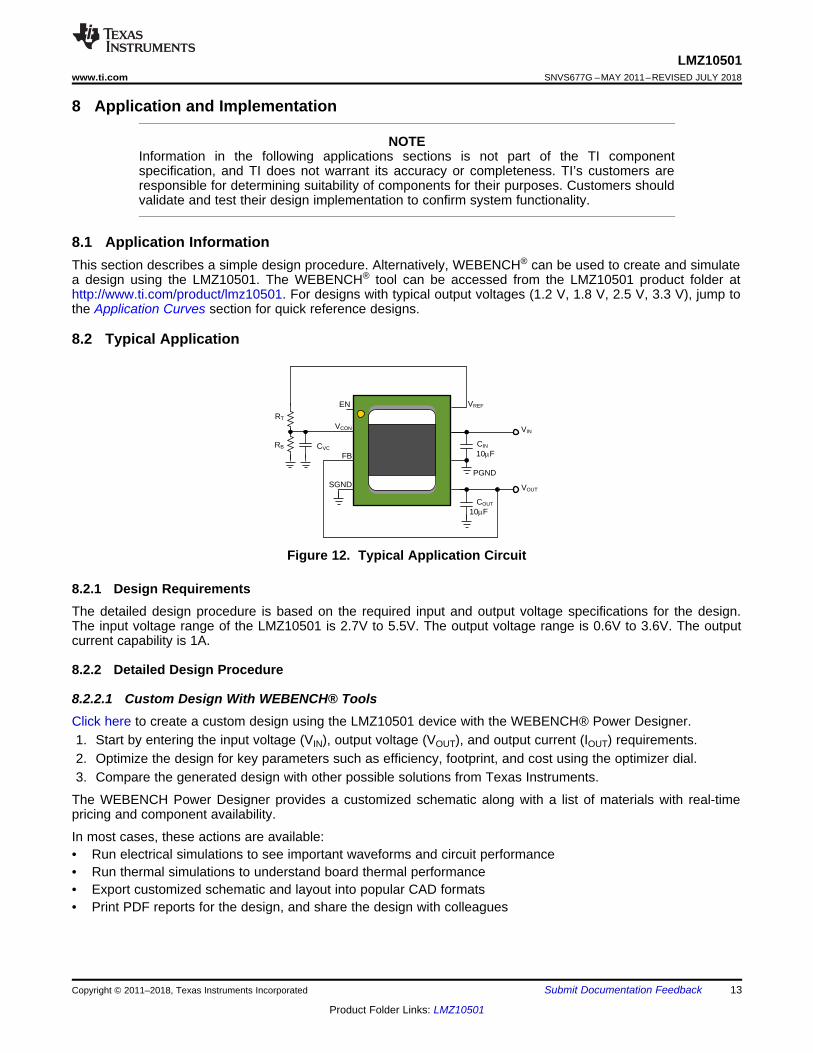
8.2 Typical Application
Figure 12. Typical Application Circuit
8.2.1 Design RequirementsThe detailed design procedure is based on the required input and output voltage specifications for the design.The input voltage range of the LMZ10501 is 2.7V to 5.5V. The output voltage range is 0.6V to 3.6V. The outputcurrent capability is 1A.
8.2.2 Detailed Design Procedure
8.2.2.1 Custom Design With WEBENCH® ToolsClick here to create a custom design using the LMZ10501 device with the WEBENCH® Power Designer.1. Start by entering the input voltage (VIN), output voltage (VOUT), and output current (IOUT) requirements.2. Optimize the design for key parameters such as efficiency, footprint, and cost using the optimizer dial.3. Compare the generated design with other possible solutions from Texas Instruments.
The WEBENCH Power Designer provides a customized schematic along with a list of materials with real-timepricing and component availability.
In most cases, these actions are available:• Run electrical simulations to see important waveforms and circuit performance• Run thermal simulations to understand board thermal performance• Export customized schematic and layout into popular CAD formats• Print PDF reports for the design, and share the design with colleagues
Typical Application (continued)8.2.2.2 Setting The Output VoltageThe LMZ10501 provides a fixed 2.35-V VREF voltage output. As shown in Figure 12 above, a resistive dividerformed by RT and RB sets the VCON pin voltage level. The VOUT voltage tracks VCON and is governed by thefollowing relationship:
VOUT = GAIN x VCON
where GAIN is 2.5V/V from VCON to VFB (1)
This equation is valid for output voltages between 0.6V and 3.6V and corresponds to VCON voltage between0.24V and 1.44V, respectively.
8.2.2.2.1 RT And RB Selection For Fixed VOUT
The parameters affecting the output voltage setting are the RT, RB, and the product of the VREF voltage × GAIN.The VREF voltage is typically 2.35V. Since VCON is derived from VREF via RT and RB,
VCON = VREF × RB/ (RB + RT) (2)
After substitution,VOUT = VREF × GAIN × RB/ (RB + RT) (3)RT = (GAIN x VREF / VOUT – 1) × RB (4)
The ideal product of GAIN × VREF = 5.875 V.
Choose RT to be between 80kΩ and 300kΩ. Then, RB can be calculated using Equation 5 below.RB = (VOUT / (5.875 V – VOUT)) × RT (5)
Note that the resistance of RT should be ≥ 80kΩ. This ensures that the VREF output current loading is notexceeded and the reference voltage is maintained. The current loading on VREF should not be greater than 30µA.
8.2.2.2.2 Output Voltage Accuracy Optimization
Each nano module is optimized to achieve high VOUT accuracy. Equation 1 shows that, by design, the outputvoltage is a function of the VCON voltage and the gain from VCON to VFB. The voltage at VCON is derived fromVREF. Therefore, as shown in Equation 3, the accuracy of the output voltage is a function of the VREF x GAINproduct as well as the tolerance of the RT and RB resistors. The typical VREF x GAIN product by design is 5.875V. Each nano module's VREF voltage is trimmed so that this product is as close to the ideal 5.875 V value aspossible, achieving high VOUT accuracy. See the Features Description section for the VREF x GAIN producttolerance limits.
8.2.2.3 Dynamic Output Voltage ScalingThe VCON pin on the LMZ10501 can be driven externally by a DAC to scale the output voltage dynamically. Theoutput voltage VOUT = 2.5 V/V x VCON. When driving VCON with a source different than VREF place a 1.5kΩ resistorin series with the VCON pin. Current limiting the external VCON helps to protect this pin and allows the VCONcapacitor to be fully discharged to 0V after fault conditions.
8.2.2.4 Integrated InductorThe LMZ10501 includes an inductor with over 1.2A DC current rating and soft saturation profile for up to 2A. Thisinductor allows for low package height and provides an easy to use, compact solution with reduced EMI.
8.2.2.5 Input And Output Capacitor SelectionThe LMZ10501 is designed for use with low ESR multi-layer ceramic capacitors (MLCC) for its input and outputfilters. Using a 10 µF 0603 or 0805 with 6.3V or 10V rating ceramic input capacitor typically provides sufficientVIN bypass. Use of multiple 4.7 µF or 2.2 µF capacitors can also be considered. Ceramic capacitors with X5Rand X7R temperature characteristics are recommended for both input and output filters. These provide anoptimal balance between small size, cost, reliability, and performance for space sensitive applications.
Typical Application (continued)The DC voltage bias characteristics of the capacitors must be considered when selecting the DC voltage ratingand case size of these components. The effective capacitance of an MLCC is typically reduced by the DCvoltage bias applied across its terminals. For example, a typical 0805 case size X5R 6.3 V 10 µF ceramiccapacitor may only have 4.8 µF left in it when a 5.0-V DC bias is applied. Similarly, a typical 0603 case size X5R6.3V 10 µF ceramic capacitor may only have 2.4 µF at the same 5.0V DC. Smaller case size capacitors mayhave even larger percentage drop in value with DC bias.
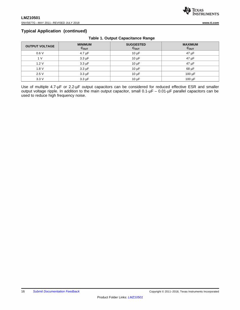
The optimum output capacitance value is application dependent. Too small output capacitance can lead toinstability due to lower loop phase margin. On the other hand, if the output capacitor is too large, it may preventthe output voltage from reaching the 0.375 V required voltage level at the end of the startup sequence. In suchcases, the output short circuit protection can be engaged and the nano module will enter a hiccup mode asdescribed in the Output Short Circuit Protection section. Table 1 sets the minimum output capacitance forstability and maximum output capacitance for proper startup for various output voltage settings. Note that themaximum COUT value in Table 1 assumes that the filter capacitance on VCON is the maximum recommendedvalue of 1nF and the RT resistor value is less than 300kΩ. Lower VCON capacitance can extend the maximumCOUT range. There is no great performance benefit in using excessive COUT values.
Typical Application (continued)Table 1. Output Capacitance Range
OUTPUT VOLTAGE MINIMUMCOUT
SUGGESTEDCOUT
MAXIMUMCOUT
0.6 V 4.7 µF 10 µF 47 µF1 V 3.3 µF 10 µF 47 µF
1.2 V 3.3 µF 10 µF 47 µF1.8 V 3.3 µF 10 µF 68 µF2.5 V 3.3 µF 10 µF 100 µF3.3 V 3.3 µF 10 µF 100 µF
Use of multiple 4.7-µF or 2.2-µF output capacitors can be considered for reduced effective ESR and smalleroutput voltage ripple. In addition to the main output capacitor, small 0.1-µF – 0.01-µF parallel capacitors can beused to reduce high frequency noise.
9.1 Voltage RangeThe voltage of the input supply must not exceed the Absolute Maximum Ratings and the RecommendedOperating Conditions of the LMZ10501.
9.2 Current CapabilityThe input supply must be able to supply the required input current to the LMZ10501 converter. The requiredinput current depends on the application's minimum required input voltage (VIN-MIN), the required output power(VOUT × IOUT-MAX), and the converter efficiency (η).
IIN = VOUT × IOUT-MAX / (VIN-MIN × η) (6)
For example, for a design with 5-V minimum input voltage,1.8-V output, and 1-A maximum load, considering 82%conversion efficiency, the required input current at steady state is 0.439 A.
9.3 Input ConnectionLong input connection cables can cause issues with the normal operation of any buck converter.
9.3.1 Voltage DropsUsing long input wires to connect the supply to the input of any converter adds impedance in series with theinput supply. This impedance can cause a voltage drop at the VIN pin of the converter when the output of theconverter is loaded. If the input voltage is near the minimum operating voltage, this added voltage drop cancause the converter to drop out or reset. If long wires are used during testing, it is recommended to add somebulk (i.e. electrolytic) capacitance at the input of the converter.
9.3.2 StabilityThe added inductance of long input cables together with the ceramic (and low ESR) input capacitor can result inan under damped RLC network at the input of the Buck converter. This can cause oscillations on the input andinstability. If long wires are used, it is recommended to add some electrolytic capacitance in parallel with theceramic input capacitor. The electrolytic capacitor's ESR will improve the damping.
Use an electrolytic capacitor with CELECTROLYTIC≥ 4 × CCERAMIC and ESRELECTROLYTIC≈ √ (LCABLE / CCERAMIC)
For example, two cables (one for VIN and one for GND), each 1 meter (~3 ft) long with ~1 mm diameter(18AWG), placed 1cm (~0.4 in) apart will form a rectangular loop resulting in about 1.2µH of inductance. Theinductance in this example can be decreased to almost half if the input wires are twisted. Based on a 10µFceramic input capacitor, the recommended parallel CELECTROLYTIC is ≥ 40 µF. Using a 47-µF capacitor will besufficient. The recommended ESRELECTROLYTIC≈ 0.35Ω or larger, based on about 1.2 µH of inductance and 10 µFof ceramic input capacitance.
See application note SNVA489 for more details on input filter design.
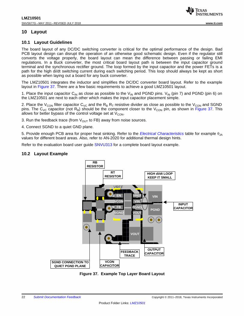
10.1 Layout GuidelinesThe board layout of any DC/DC switching converter is critical for the optimal performance of the design. BadPCB layout design can disrupt the operation of an otherwise good schematic design. Even if the regulator stillconverts the voltage properly, the board layout can mean the difference between passing or failing EMIregulations. In a Buck converter, the most critical board layout path is between the input capacitor groundterminal and the synchronous rectifier ground. The loop formed by the input capacitor and the power FETs is apath for the high di/dt switching current during each switching period. This loop should always be kept as shortas possible when laying out a board for any buck converter.
The LMZ10501 integrates the inductor and simplifies the DC/DC converter board layout. Refer to the examplelayout in Figure 37. There are a few basic requirements to achieve a good LMZ10501 layout.
1. Place the input capacitor CIN as close as possible to the VIN and PGND pins. VIN (pin 7) and PGND (pin 6) onthe LMZ10501 are next to each other which makes the input capacitor placement simple.
2. Place the VCON filter capacitor CVC and the RB RT resistive divider as close as possible to the VCON and SGNDpins. The CVC capacitor (not RB) should be the component closer to the VCON pin, as shown in Figure 37. Thisallows for better bypass of the control voltage set at VCON.
3. Run the feedback trace (from VOUT to FB) away from noise sources.
4. Connect SGND to a quiet GND plane.
5. Provide enough PCB area for proper heat sinking. Refer to the Electrical Characteristics table for example θJAvalues for different board areas. Also, refer to AN-2020 for additional thermal design hints.
Refer to the evaluation board user guide SNVU313 for a complete board layout example.
10.3 Package ConsiderationsUse the following recommendations when utilizing machine placement :• Use 1.06 mm (42mil) or smaller nozzle size. The pick up area is the top of the inductor which is 1.6 mm × 2
mm.• Soft tip pick and place nozzle is recommended.• Add 0.05 mm to the component thickness so that the device will be released 0.05 mm (2 mil) into the solder
paste without putting pressure or splashing the solder paste.• Slow the pick arm when picking the part from the tape and reel carrier and when depositing the IC on the
board.• If the machine releases the component by force, use minimum force or no more than 3 Newtons.
For manual placement:• Use a vacuum pick up hand tool with soft tip head.• If vacuum pick up tool is not available, use non-metal tweezers and hold the part by sides.• Use minimal force when picking and placing the module on the board.• Using hot air station provides better temperature control and better controlled air flow than a heat gun.• Go to the video section at www.ti.com/product/lmz10501 for a quick video on how to solder rework the
11.1.1 Custom Design With WEBENCH® ToolsClick here to create a custom design using the LMZ10501 device with the WEBENCH® Power Designer.1. Start by entering the input voltage (VIN), output voltage (VOUT), and output current (IOUT) requirements.2. Optimize the design for key parameters such as efficiency, footprint, and cost using the optimizer dial.3. Compare the generated design with other possible solutions from Texas Instruments.
The WEBENCH Power Designer provides a customized schematic along with a list of materials with real-timepricing and component availability.
In most cases, these actions are available:• Run electrical simulations to see important waveforms and circuit performance• Run thermal simulations to understand board thermal performance• Export customized schematic and layout into popular CAD formats• Print PDF reports for the design, and share the design with colleagues
Get more information about WEBENCH tools at www.ti.com/WEBENCH.
11.2 Documentation Support
11.2.1 Related Documentation• AN-2162 Simple Success With Conducted EMI From DC- DC Converters•• LMZ10501SIL and LMZ10500SIL SIMPLE SWITCHER® Nano Module Evaluation Board
11.3 Receiving Notification of Documentation UpdatesTo receive notification of documentation updates, navigate to the device product folder on ti.com. In the upperright corner, click on Alert me to register and receive a weekly digest of any product information that haschanged. For change details, review the revision history included in any revised document.
11.4 Community ResourcesThe following links connect to TI community resources. Linked contents are provided "AS IS" by the respectivecontributors. They do not constitute TI specifications and do not necessarily reflect TI's views; see TI's Terms ofUse.
TI E2E™ Online Community TI's Engineer-to-Engineer (E2E) Community. Created to foster collaborationamong engineers. At e2e.ti.com, you can ask questions, share knowledge, explore ideas and helpsolve problems with fellow engineers.
Design Support TI's Design Support Quickly find helpful E2E forums along with design support tools andcontact information for technical support.
11.5 TrademarksE2E is a trademark of Texas Instruments.WEBENCH is a registered trademark of Texas Instruments.All other trademarks are the property of their respective owners.
11.6 Electrostatic Discharge CautionThese devices have limited built-in ESD protection. The leads should be shorted together or the device placed in conductive foamduring storage or handling to prevent electrostatic damage to the MOS gates.
This glossary lists and explains terms, acronyms, and definitions.
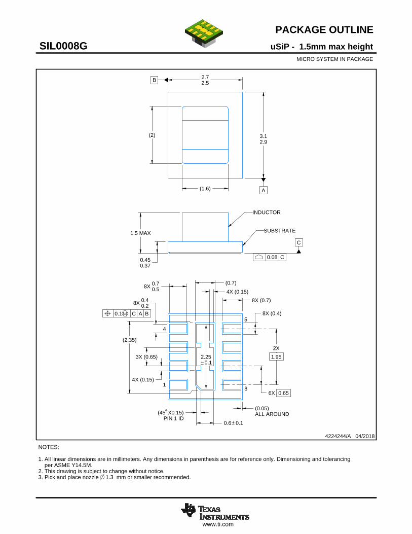
12 Mechanical, Packaging, and Orderable InformationThe following pages include mechanical, packaging, and orderable information. This information is the mostcurrent data available for the designated devices. This data is subject to change without notice and revision ofthis document. For browser-based versions of this data sheet, refer to the left-hand navigation.
uSiP - 1.5mm max heightSIL0008GMICRO SYSTEM IN PACKAGE
4224244/A 04/2018
0.08 C
INDUCTOR
SUBSTRATE
0.1 C A B
1
4
5
8
NOTES: 1. All linear dimensions are in millimeters. Any dimensions in parenthesis are for reference only. Dimensioning and tolerancing per ASME Y14.5M.2. This drawing is subject to change without notice. 3. Pick and place nozzle 1.3 mm or smaller recommended.
SCALE 5.000
www.ti.com
EXAMPLE BOARD LAYOUT
(0.6)
8X (0.6)
2X ( 0.2)VIA
0.07 MAXALL AROUND
0.07 MINALL AROUND
8X (0.3)
(1.9)
(1.95)
6X(0.65)
(2.25) (0.41)
uSiP - 1.5mm max heightSIL0008GMICRO SYSTEM IN PACKAGE
4224244/A 04/2018
SYMM
SYMM
SEE DETAILS
1
45
8
LAND PATTERN EXAMPLE1:1 RATIO WITH PACKAGE SOLDER PADS
SCALE: 20X
SOLDER MASK DETAILSNOT TO SCALE
NOTES: (continued) 4. This package is designed to be soldered to a thermal pad on the board. For more information, see Texas Instruments literature number SLUA271 (www.ti.com/lit/slua271).
METAL EDGE
SOLDER MASKOPENING
NON SOLDER MASKDEFINED
EXPOSEDMETAL METAL
SOLDERMASKOPENING
SOLDER MASKDEFINED
EXPOSEDMETAL
www.ti.com
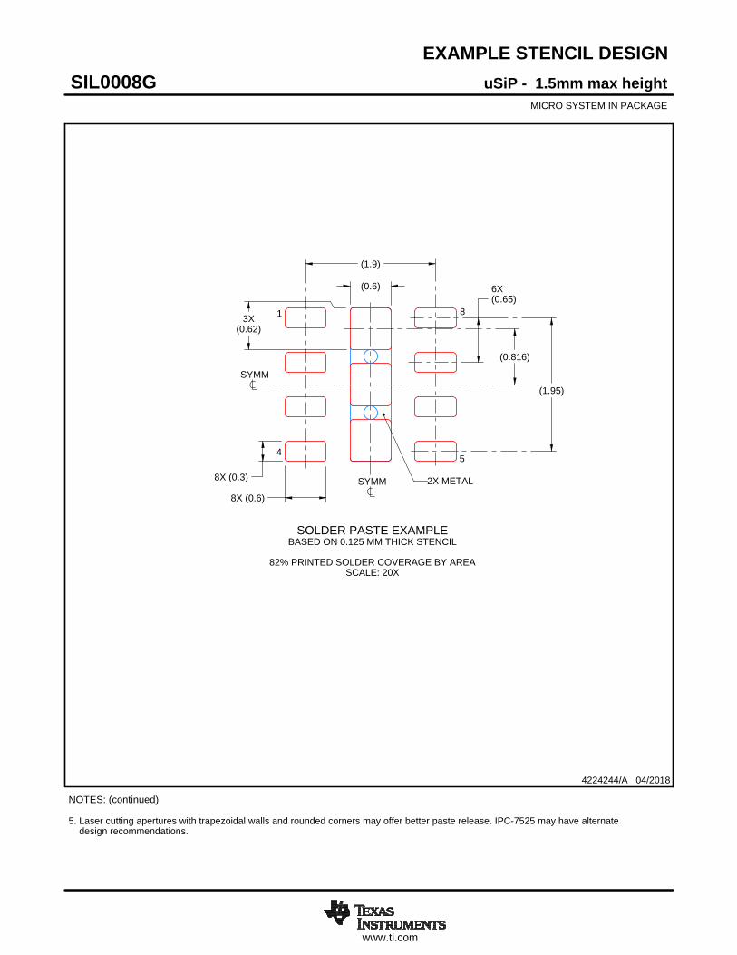
EXAMPLE STENCIL DESIGN
(0.6)
(1.95)
(1.9)
3X(0.62)
8X (0.3)
8X (0.6)
6X(0.65)
(0.816)
uSiP - 1.5mm max heightSIL0008GMICRO SYSTEM IN PACKAGE
4224244/A 04/2018
NOTES: (continued) 5. Laser cutting apertures with trapezoidal walls and rounded corners may offer better paste release. IPC-7525 may have alternate design recommendations.
SYMM
SYMM 2X METAL
1
45
8
SOLDER PASTE EXAMPLEBASED ON 0.125 MM THICK STENCIL
82% PRINTED SOLDER COVERAGE BY AREA
SCALE: 20X
PACKAGE OPTION ADDENDUM
www.ti.com 30-Jun-2018
Addendum-Page 1
PACKAGING INFORMATION
Orderable Device Status(1)
Package Type PackageDrawing
Pins PackageQty
Eco Plan(2)
Lead/Ball Finish(6)
MSL Peak Temp(3)
Op Temp (°C) Device Marking(4/5)
Samples
LMZ10501SILR ACTIVE uSiP SIL 8 3000 Green (RoHS& no Sb/Br)
NIAU Level-3-260C-168 HR -40 to 125 TXN5010EC(501, DG)981105010501 9811 DG
LMZ10501SILT ACTIVE uSiP SIL 8 250 Green (RoHS& no Sb/Br)
NIAU Level-3-260C-168 HR -40 to 125 TXN5010EC(501, DG)981105010501 9811 DG
(1) The marketing status values are defined as follows:ACTIVE: Product device recommended for new designs.LIFEBUY: TI has announced that the device will be discontinued, and a lifetime-buy period is in effect.NRND: Not recommended for new designs. Device is in production to support existing customers, but TI does not recommend using this part in a new design.PREVIEW: Device has been announced but is not in production. Samples may or may not be available.OBSOLETE: TI has discontinued the production of the device.
(2) RoHS: TI defines "RoHS" to mean semiconductor products that are compliant with the current EU RoHS requirements for all 10 RoHS substances, including the requirement that RoHS substancedo not exceed 0.1% by weight in homogeneous materials. Where designed to be soldered at high temperatures, "RoHS" products are suitable for use in specified lead-free processes. TI mayreference these types of products as "Pb-Free".RoHS Exempt: TI defines "RoHS Exempt" to mean products that contain lead but are compliant with EU RoHS pursuant to a specific EU RoHS exemption.Green: TI defines "Green" to mean the content of Chlorine (Cl) and Bromine (Br) based flame retardants meet JS709B low halogen requirements of <=1000ppm threshold. Antimony trioxide basedflame retardants must also meet the <=1000ppm threshold requirement.
(3) MSL, Peak Temp. - The Moisture Sensitivity Level rating according to the JEDEC industry standard classifications, and peak solder temperature.
(4) There may be additional marking, which relates to the logo, the lot trace code information, or the environmental category on the device.
(5) Multiple Device Markings will be inside parentheses. Only one Device Marking contained in parentheses and separated by a "~" will appear on a device. If a line is indented then it is a continuationof the previous line and the two combined represent the entire Device Marking for that device.
(6) Lead/Ball Finish - Orderable Devices may have multiple material finish options. Finish options are separated by a vertical ruled line. Lead/Ball Finish values may wrap to two lines if the finishvalue exceeds the maximum column width.
Important Information and Disclaimer:The information provided on this page represents TI's knowledge and belief as of the date that it is provided. TI bases its knowledge and belief on informationprovided by third parties, and makes no representation or warranty as to the accuracy of such information. Efforts are underway to better integrate information from third parties. TI has taken andcontinues to take reasonable steps to provide representative and accurate information but may not have conducted destructive testing or chemical analysis on incoming materials and chemicals.TI and TI suppliers consider certain information to be proprietary, and thus CAS numbers and other limited information may not be available for release.
In no event shall TI's liability arising out of such information exceed the total purchase price of the TI part(s) at issue in this document sold by TI to Customer on an annual basis.
IMPORTANT NOTICE
Texas Instruments Incorporated (TI) reserves the right to make corrections, enhancements, improvements and other changes to itssemiconductor products and services per JESD46, latest issue, and to discontinue any product or service per JESD48, latest issue. Buyersshould obtain the latest relevant information before placing orders and should verify that such information is current and complete.TI’s published terms of sale for semiconductor products (http://www.ti.com/sc/docs/stdterms.htm) apply to the sale of packaged integratedcircuit products that TI has qualified and released to market. Additional terms may apply to the use or sale of other types of TI products andservices.Reproduction of significant portions of TI information in TI data sheets is permissible only if reproduction is without alteration and isaccompanied by all associated warranties, conditions, limitations, and notices. TI is not responsible or liable for such reproduceddocumentation. Information of third parties may be subject to additional restrictions. Resale of TI products or services with statementsdifferent from or beyond the parameters stated by TI for that product or service voids all express and any implied warranties for theassociated TI product or service and is an unfair and deceptive business practice. TI is not responsible or liable for any such statements.Buyers and others who are developing systems that incorporate TI products (collectively, “Designers”) understand and agree that Designersremain responsible for using their independent analysis, evaluation and judgment in designing their applications and that Designers havefull and exclusive responsibility to assure the safety of Designers' applications and compliance of their applications (and of all TI productsused in or for Designers’ applications) with all applicable regulations, laws and other applicable requirements. Designer represents that, withrespect to their applications, Designer has all the necessary expertise to create and implement safeguards that (1) anticipate dangerousconsequences of failures, (2) monitor failures and their consequences, and (3) lessen the likelihood of failures that might cause harm andtake appropriate actions. Designer agrees that prior to using or distributing any applications that include TI products, Designer willthoroughly test such applications and the functionality of such TI products as used in such applications.TI’s provision of technical, application or other design advice, quality characterization, reliability data or other services or information,including, but not limited to, reference designs and materials relating to evaluation modules, (collectively, “TI Resources”) are intended toassist designers who are developing applications that incorporate TI products; by downloading, accessing or using TI Resources in anyway, Designer (individually or, if Designer is acting on behalf of a company, Designer’s company) agrees to use any particular TI Resourcesolely for this purpose and subject to the terms of this Notice.TI’s provision of TI Resources does not expand or otherwise alter TI’s applicable published warranties or warranty disclaimers for TIproducts, and no additional obligations or liabilities arise from TI providing such TI Resources. TI reserves the right to make corrections,enhancements, improvements and other changes to its TI Resources. TI has not conducted any testing other than that specificallydescribed in the published documentation for a particular TI Resource.Designer is authorized to use, copy and modify any individual TI Resource only in connection with the development of applications thatinclude the TI product(s) identified in such TI Resource. NO OTHER LICENSE, EXPRESS OR IMPLIED, BY ESTOPPEL OR OTHERWISETO ANY OTHER TI INTELLECTUAL PROPERTY RIGHT, AND NO LICENSE TO ANY TECHNOLOGY OR INTELLECTUAL PROPERTYRIGHT OF TI OR ANY THIRD PARTY IS GRANTED HEREIN, including but not limited to any patent right, copyright, mask work right, orother intellectual property right relating to any combination, machine, or process in which TI products or services are used. Informationregarding or referencing third-party products or services does not constitute a license to use such products or services, or a warranty orendorsement thereof. Use of TI Resources may require a license from a third party under the patents or other intellectual property of thethird party, or a license from TI under the patents or other intellectual property of TI.TI RESOURCES ARE PROVIDED “AS IS” AND WITH ALL FAULTS. TI DISCLAIMS ALL OTHER WARRANTIES ORREPRESENTATIONS, EXPRESS OR IMPLIED, REGARDING RESOURCES OR USE THEREOF, INCLUDING BUT NOT LIMITED TOACCURACY OR COMPLETENESS, TITLE, ANY EPIDEMIC FAILURE WARRANTY AND ANY IMPLIED WARRANTIES OFMERCHANTABILITY, FITNESS FOR A PARTICULAR PURPOSE, AND NON-INFRINGEMENT OF ANY THIRD PARTY INTELLECTUALPROPERTY RIGHTS. TI SHALL NOT BE LIABLE FOR AND SHALL NOT DEFEND OR INDEMNIFY DESIGNER AGAINST ANY CLAIM,INCLUDING BUT NOT LIMITED TO ANY INFRINGEMENT CLAIM THAT RELATES TO OR IS BASED ON ANY COMBINATION OFPRODUCTS EVEN IF DESCRIBED IN TI RESOURCES OR OTHERWISE. IN NO EVENT SHALL TI BE LIABLE FOR ANY ACTUAL,DIRECT, SPECIAL, COLLATERAL, INDIRECT, PUNITIVE, INCIDENTAL, CONSEQUENTIAL OR EXEMPLARY DAMAGES INCONNECTION WITH OR ARISING OUT OF TI RESOURCES OR USE THEREOF, AND REGARDLESS OF WHETHER TI HAS BEENADVISED OF THE POSSIBILITY OF SUCH DAMAGES.Unless TI has explicitly designated an individual product as meeting the requirements of a particular industry standard (e.g., ISO/TS 16949and ISO 26262), TI is not responsible for any failure to meet such industry standard requirements.Where TI specifically promotes products as facilitating functional safety or as compliant with industry functional safety standards, suchproducts are intended to help enable customers to design and create their own applications that meet applicable functional safety standardsand requirements. Using products in an application does not by itself establish any safety features in the application. Designers mustensure compliance with safety-related requirements and standards applicable to their applications. Designer may not use any TI products inlife-critical medical equipment unless authorized officers of the parties have executed a special contract specifically governing such use.Life-critical medical equipment is medical equipment where failure of such equipment would cause serious bodily injury or death (e.g., lifesupport, pacemakers, defibrillators, heart pumps, neurostimulators, and implantables). Such equipment includes, without limitation, allmedical devices identified by the U.S. Food and Drug Administration as Class III devices and equivalent classifications outside the U.S.TI may expressly designate certain products as completing a particular qualification (e.g., Q100, Military Grade, or Enhanced Product).Designers agree that it has the necessary expertise to select the product with the appropriate qualification designation for their applicationsand that proper product selection is at Designers’ own risk. Designers are solely responsible for compliance with all legal and regulatoryrequirements in connection with such selection.Designer will fully indemnify TI and its representatives against any damages, costs, losses, and/or liabilities arising out of Designer’s non-compliance with the terms and provisions of this Notice.