LNK603-606/613-616 LinkSwitch-II Family www.power.com October 2020 Energy-Efficient, Accurate CV/CC Switcher for Adapters and Chargers This Product is Covered by Patents and/or Pending Patent Applications. Output Power Table Product 3 85-265 VAC Adapter 1 Open Frame 2 LNK603/613PG/DG 2.5 W 3.3 W LNK604/614PG/DG 3.5 W 4.1 W LNK605/615PG/DG 4.5 W 5.1 W LNK606/616PG/GG/DG 5.5 W 6.1 W Table 1. Output Power Table. Notes: 1. Minimum continuous power in a typical non-ventilated enclosed adapter measured at +50 °C ambient, device, T J <100 °C. 2. Maximum practical continuous power in an open frame design with adequate heat sinking, measured at 50 °C ambient (see Key Applications Consider- ations section for more information). 3. Packages: P: DIP-8C, G: SMD-8C, D: SO-8C. Product Highlights Dramatically Simplifies CV/CC Converters • Eliminates optocoupler and all secondary CV/CC control circuitry • Eliminates all control loop compensation circuitry Advanced Performance Features • Compensates for transformer inductance tolerances • Compensates for input line voltage variations • Compensates for cable voltage drop (LNK61X series) • Compensates for external component temperature variations • Very tight IC parameter tolerances using proprietary trimming technology • Frequency jittering greatly reduces EMI filter cost • Even tighter output tolerances achievable with external resistor selection/trimming • Programmable switching frequency up to 85 kHz to reduce trans- former size Advanced Protection/Safety Features • Auto-restart protection reduces power delivered by >95% for output short-circuit and control loop faults (open and shorted components) • Hysteretic thermal shutdown – automatic recovery reduces power supply returns from the field • Meets high-voltage creepage requirements between DRAIN and all other pins both on the PCB and at the package EcoSmart™– Energy Efficient • Easily meets all global energy efficiency regulations • No-load consumption below 30 mW at 230 VAC with optional external bias winding • ON/OFF control provides constant efficiency down to very light loads – ideal for CEC and ENERGY STAR 2.0 regulations • No current sense resistors – maximizes efficiency Green Package • Halogen free and RoHS compliant package Applications • Chargers for cell/cordless phones, PDAs, MP3/portable audio devices, adapters, LED drivers, etc. Description The LinkSwitch™-II dramatically simplifies low power CV/CC charger designs by eliminating an optocoupler and secondary control circuitry. The device introduces a revolutionary control technique to provide very tight output voltage and current regulation, compensating for transformer and internal parameter tolerances along with input voltage variations. The device incorporates a 700 V power MOSFET, a novel ON/OFF control state machine, a high-voltage switched current source for self biasing, frequency jittering, cycle-by-cycle current limit and hysteretic thermal shutdown circuitry onto a monolithic IC. Figure 1. Typical Application/Performance – Not a Simplified Circuit (a) and Output Characteristic Envelope (b). (see Application Section for more information). I O V O ±5% ±10% PI-4906-012315 (a) Typical Application Schematic (b) Output Characteristic Figure 2. Package Options. DIP-8C (P Package) SMD-8C (G Package) SO-8C (D Package). LinkSwitch-II Wide Range High-Voltage DC Input PI-4960-012315 D S FB BP/M
Transcript
LNK603-606/613-616 LinkSwitch-II Family
www.power.com October 2020
Energy-Efficient, Accurate CV/CC Switcherfor Adapters and Chargers
This Product is Covered by Patents and/or Pending Patent Applications.
Output Power Table
Product385-265 VAC
Adapter1 Open Frame2
LNK603/613PG/DG 2.5 W 3.3 W
LNK604/614PG/DG 3.5 W 4.1 W
LNK605/615PG/DG 4.5 W 5.1 W
LNK606/616PG/GG/DG 5.5 W 6.1 W
Table 1. Output Power Table. Notes: 1. Minimum continuous power in a typical non-ventilated enclosed adapter
measured at +50 °C ambient, device, TJ <100 °C.2. Maximum practical continuous power in an open frame design with adequate
heat sinking, measured at 50 °C ambient (see Key Applications Consider-ations section for more information).
3. Packages: P: DIP-8C, G: SMD-8C, D: SO-8C.
Product HighlightsDramatically Simplifies CV/CC Converters• Eliminates optocoupler and all secondary CV/CC control circuitry• Eliminates all control loop compensation circuitry
Advanced Performance Features• Compensates for transformer inductance tolerances• Compensates for input line voltage variations• Compensates for cable voltage drop (LNK61X series)• Compensates for external component temperature variations• Very tight IC parameter tolerances using proprietary trimming
technology • Frequency jittering greatly reduces EMI filter cost• Even tighter output tolerances achievable with external resistor
selection/trimming• Programmable switching frequency up to 85 kHz to reduce trans-
former size
Advanced Protection/Safety Features• Auto-restart protection reduces power delivered by >95% for output
short-circuit and control loop faults (open and shorted components)• Hysteretic thermal shutdown – automatic recovery reduces power
supply returns from the field• Meets high-voltage creepage requirements between DRAIN and all
other pins both on the PCB and at the package
EcoSmart™– Energy Efficient• Easily meets all global energy efficiency regulations• No-load consumption below 30 mW at 230 VAC with optional
external bias winding • ON/OFF control provides constant efficiency down to very light loads
– ideal for CEC and ENERGY STAR 2.0 regulations• No current sense resistors – maximizes efficiency
Green Package• Halogen free and RoHS compliant package
Applications• Chargers for cell/cordless phones, PDAs, MP3/portable audio
devices, adapters, LED drivers, etc.
DescriptionThe LinkSwitch™-II dramatically simplifies low power CV/CC charger designs by eliminating an optocoupler and secondary control circuitry. The device introduces a revolutionary control technique to provide very tight output voltage and current regulation, compensating for transformer and internal parameter tolerances along with input voltage variations.
The device incorporates a 700 V power MOSFET, a novel ON/OFF control state machine, a high-voltage switched current source for self biasing, frequency jittering, cycle-by-cycle current limit and hysteretic thermal shutdown circuitry onto a monolithic IC.
Figure 1. Typical Application/Performance – Not a Simplified Circuit (a) and Output Characteristic Envelope (b). (see Application Section for more information).
Pin Functional DescriptionDRAIN (D) Pin:This pin is the power MOSFET drain connection. It provides internal operating current for both start-up and steady-state operation.
BYPASS/MULTI-FUNCTIONAL PROGRAMMABLE (BP/M) Pin:This pin has multiple functions:1. It is the connection point for an external bypass capacitor for the
internally generated 6 V supply.2. It is a mode selection for the cable drop compensation for
LNK61X series.
FEEDBACK (FB) Pin:During normal operation, switching of the power MOSFET is controlled by this pin. This pin senses the AC voltage on the bias winding. This control input regulates both the output voltage in CV mode and output current in CC mode based on the flyback voltage of the bias winding. The internal inductance correction circuit uses the forward voltage on the bias winding to sense the bulk capacitor voltage.
SOURCE (S) Pin:This pin is internally connected to the output MOSFET source for high-voltage power and control circuit common returns.
Figure 3. Functional Block Diagram.
Figure 4. Pin Configuration.
PI-4908-012915
SOURCE(S)
LEADINGEDGE
BLANKING
+
-
+
-+
-
DRAIN(D)
REGULATOR6 VBYPASS
(BP/M)
FEEDBACK(FB)
SOURCE(S)
FBOUT Reset
6 V5 V
tSAMPLE-OUT
tSAMPLE-INPUT
VILIMITILIM
VILIMIT
VTH
tSAMPLE-OUT
tSAMPLE-INPUT
VILIMIT
6.5 V
DriveILIM
DCMAX
DCMAX
FB
Current LimitComparator
STATEMACHINE
CABLE DROPCOMPENSATION
SAMPLEDELAY
THERMALSHUTDOWN
OSCILLATOR
FAULTAuto-RestartOpen-Loop
INDUCTANCECORRECTION
CONSTANTCURRENT
D Q
PI-3491-020615
D S
BP/M S
SFB
P Package (DIP-8C)G Package (SMD-8C) D Package (SO-8C)
LinkSwitch-II Functional DescriptionThe LinkSwitch-II combines a high-voltage power MOSFETswitch with a power supply controller in one device. Similar to the LinkSwitch-LP and TinySwitch-III it uses ON/OFF control to regulate the output voltage. In addition, the switching frequency is modulated to regulate the output current to provide a constant current characteristic. The LinkSwitch-II controller consists of an oscillator, feedback (sense and logic) circuit, 6 V regulator, over-temperature protection, frequency jittering, current limit circuit, leading-edge blanking, inductance correction circuitry, frequency control for constant current regulation and ON/OFF state machine for CV control.
Inductance Correction CircuitryIf the primary magnetizing inductance is either too high or low the converter will automatically compensate for this by adjusting the oscillator frequency. Since this controller is designed to operate in discontinuous-conduction mode the output power is directly proportional to the set primary inductance and its tolerance can be completely compensated with adjustments to the switching frequency.
Constant Current (CC) OperationAs the output voltage and therefore the flyback voltage across the bias winding increases, the FEEDBACK pin voltage increases. The switching frequency is adjusted as the FEEDBACK pin voltage increases to provide a constant output current regulation. The constant current circuit and the inductance correction circuit are designed to operate concurrently in the CC region.
Constant Voltage (CV) OperationAs the FEEDBACK pin approaches VFBth from the constant current regulation mode, the power supply transitions into CV operation. The switching frequency at this point is at its maximum value, corresponding to the peak power point of the CC/CV characteristic. The controller regulates the FEEDBACK pin voltage to remain at VFBth using an ON/OFF state-machine. The FEEDBACK pin voltage is sampled 2.5 ms after the turn-off of the high-voltage switch. At light loads the current limit is also reduced to decrease the transformer flux density.
Output Cable CompensationThis compensation provides a constant output voltage at the end of the cable over the entire load range in CV mode. As the converter load increases from no-load to the peak power point (transition point between CV and CC) the voltage drop introduced across the output cable is compensated by increasing the FEEDBACK pin reference voltage. The controller determines the output load and therefore the correct degree of compensation based on the output of the state machine. Cable drop compensation for a 24 AWG (0.3 W) cable is selected with CBP = 1 mF and for a 26 AWG (0.49 W) cable with CPB = 10 mF.
Auto-Restart and Open-Loop ProtectionIn the event of a fault condition such as an output short or an open loop condition the LinkSwitch-II enters into an appropriate protection mode as described below.
In the event the FEEDBACK pin voltage during the flyback period falls below 0.7 V before the FEEDBACK pin sampling delay (~2.5 ms) for a duration in excess of ~450 ms (auto-restart on-time (tAR-ON) the converter enters into auto-restart, wherein the power MOSFET is disabled for 2 seconds (~18% auto-restart duty cycle). The auto-restart alternately enables and disables the switching of the power MOSFET until the fault condition is removed.
In addition to the conditions for auto-restart described above, if the sensed FEEDBACK pin current during the forward period of the conduction cycle (switch “on” time) falls below 120 mA, the converter annunciates this as an open-loop condition (top resistor in potential divider is open or missing) and reduces the auto-restart time from 450 ms to approximately 6 clock cycles (90 ms), whilst keeping the disable period of 2 seconds.
Over-Temperature ProtectionThe thermal shutdown circuitry senses the die temperature. The threshold is set at 142 °C typical with a 60 °C hysteresis. When the die temperature rises above this threshold (142 °C) the power MOSFET is disabled and remains disabled until the die temperature falls by 60 °C, at which point the MOSFET is re-enabled.
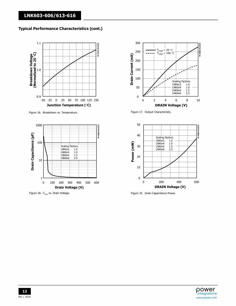
Current LimitThe current limit circuit senses the current in the power MOSFET. When this current exceeds the internal threshold (ILIMIT), the power MOSFET is turned off for the remainder of that cycle. The leading edge blanking circuit inhibits the current limit comparator for a short time (tLEB) after the power MOSFET is turned on. This leading edge blanking time has been set so that current spikes caused by capacitance and rectifier reverse recovery time will not cause premature termination of the MOSFET conduction. The LinkSwitch-II also contains a “di/dt” correction feature to minimize CC variation across the input line range.
6.0 V RegulatorThe 6 V regulator charges the bypass capacitor connected to the BYPASS pin to 6 V by drawing a current from the voltage on the DRAIN, whenever the MOSFET is off. The BYPASS pin is the internal supply voltage node. When the MOSFET is on, the device runs off of the energy stored in the bypass capacitor. Extremely low power consumption of the internal circuitry allows the LinkSwitch-II to operate continuously from the current drawn from the DRAIN pin. A bypass capacitor value of either 1 mF or 10 mF is sufficient for both high frequency decoupling and energy storage.
This circuit shown in Figure 5 is configured as a primary-side regulated flyback power supply utilizing the LNK613DG. With an average efficiency of 74% and <30 mW no-load input power this design easily exceeds the most stringent current energy efficiency requirements.
Input FilterAC input power is rectified by diodes D1 through D4. The rectified DC is filtered by the bulk storage capacitors C1 and C2. Inductor L1, C1 and C2 form a pi (π) filter, which attenuates conducted differential-mode EMI noise. This configuration along with Power Integrations transformer E-shield™ technology allow this design to meet EMI standard EN55022 class B with good margin without requiring a Y capacitor, even with the output connected to safety earth ground. Fusible resistor RF1 provides protection against catastrophic failure. This should be suitably rated (typically a wire wound type) to withstand the instantaneous dissipation while the input capacitors charge when first connected to the AC line.
LNK 613 PrimaryThe LNK613DG device (U1) incorporates the power switching device, oscillator, CC/CV control engine, startup, and protection functions. The integrated 700 V MOSFET provides a large drain voltage margin in universal input AC applications, increasing reliability and also reducing the output diode voltage stress by allowing a greater transformer turns ratio. The device is completely self-powered from the BYPASS pin and decoupling capacitor C4. For the LNK61X devices, the bypass capacitor value also selects the amount of output cable voltage drop compensation. A 1 mF value selects the standard compensation. A 10 mF value selects the enhanced compensation.
Table 2 shows the amount of compensation for each device and bypass capacitor value. The LNK60x devices do not provide cable drop compensation.
The optional bias supply formed by D6 and C5 provides the operating current for U1 via resistor R4. This reduces the no-load consumption from ~200 mW to <30 mW and also increases light load efficiency.
The rectified and filtered input voltage is applied to one side of the primary winding of T1. The other side of the transformer’s primary winding is driven by the integrated MOSFET in U1. The leakage inductance drain voltage spike is limited by an RCD-R clamp consisting of D5, R2, R3, and C3.
Output RectificationThe secondary of the transformer is rectified by D7, a 1 A, 40 V Schottky barrier type for higher efficiency, and filtered by C7. If lower efficiency is acceptable then this can be replaced with a 1 A PN junction diode for lower cost. In this application C7 was sized to meet the required output voltage ripple specification without requiring a post LC filter. To meet battery self discharge requirement the pre-load resistor has been replaced with a series resistor and Zener network (R8 and VR1). However in designs where this is not a requirement a standard 1 kW resistor can be used.
Output RegulationThe LNK613 regulates the output using ON/OFF control in the constant voltage (CV) regulation region of the output character-istic and frequency control for constant current (CC) regulation. The feedback resistors (R5 and R6) were selected using standard 1% resistor values to center both the nominal output voltage and constant current regulation thresholds.
Figure 5. Energy Efficient USB Charger Power Supply (74% Average Efficiency, <30 mW No-load Input Power).
The data sheet maximum output power table (Table 1) repre-sents the maximum practical continuous output power level that can be obtained under the following assumed conditions:
1. The minimum DC input voltage is 90 V or higher at 85 VAC input. The value of the input capacitance should be large enough to meet these criteria for AC input designs.
2. Secondary output of 5 V with a Schottky rectifier diode.3. Assumed efficiency of 70%.4. Discontinuous mode operation (KP >1.3).5. The part is board mounted with SOURCE pins soldered to a
sufficient area of copper to keep the SOURCE pin temperature at or below 90 °C.
6. Ambient temperature of 50 °C for open frame designs and an internal enclosure temperature of 60 °C for adapter designs.
Note: Higher output power are achievable if an output CC tolerance >±10% is acceptable, allowing the device to be operated at a higher SOURCE pin temperature.
Output Tolerance
LinkSwitch-II provides an overall output tolerance (including line, component variation and temperature) of ±5% for the output voltage in CV operation and ±10% for the output current during CC operation over a junction temperature range of 0 °C to 100 °C for the P/G package. For the D package (SO8) additional CC variance may occur due to stress caused by the manufacturing flow (i.e. solder-wave immersion or IR reflow). A sample power supply build is recommended to verify production tolerances for each design.
BYPASS Pin Capacitor Selection
For LinkSwitch-II 60x Family of Devices (without output cable voltage drop compensation)A 1 mF BYPASS pin capacitor is recommended. The capacitor voltage rating should be greater than 7 V. The capacitor’s dielectric material is not important but tolerance of capacitor should be ≤ ±50%. The capacitor must be physically located close to the LinkSwitch-II BYPASS pin.
For LinkSwitch-II 61x Family of Devices (with output cable voltage drop compensation)The amount of output cable compensation can be selected with the value of the BYPASS pin capacitor. A value of 1 mF selects the standard cable compensation. A 10 mF capacitor selects the enhanced cable compensation. Table 2 shows the amount of compensation for each LinkSwitch-II device and capacitor value. The capacitor can be either ceramic or electrolytic but tolerance and temperature variation should be ≤ ±50%.
The output voltage that is entered into PIXls design spreadsheet is the voltage at the end of the output cable when the power supply is delivering maximum power. The output voltage at the terminals of the supply is the value measured at the end of the cable multiplied by the output voltage change factor.
LinkSwitch-II Layout Considerations
Circuit Board LayoutLinkSwitch-II is a highly integrated power supply solution that integrates on a single die, both, the controller and the high-voltage MOSFET. The presence of high switching currents and voltages together with analog signals makes it especially important to follow good PCB design practice to ensure stable and trouble free operation
of the power supply. See Figure 6 for a recommended circuit board layout for LinkSwitch-II.
When designing a printed circuit board for the LinkSwitch-II based power supply, it is important to follow the following guidelines:
Single Point GroundingUse a single point (Kelvin) connection at the negative terminal of the input filter capacitor for the LinkSwitch-II SOURCE pin and bias winding return. This improves surge capabilities by returning surge currents from the bias winding directly to the input filter capacitor.
Bypass CapacitorThe BYPASS pin capacitor should be located as close as possible to the SOURCE and BYPASS pins.
Feedback ResistorsPlace the feedback resistors directly at the FEEDBACK pin of the LinkSwitch-II device. This minimizes noise coupling.
Thermal ConsiderationsThe copper area connected to the SOURCE pins provides the LinkSwitch-II heat sink. A good estimate is that the LinkSwitch-II will dissipate 10% of the output power. Provide enough copper area to keep the SOURCE pin temperature below 90 °C. Higher temperatures are allowable only if an output current (CC) tolerance above ±10% is acceptable. In this case a maximum SOURCE pin temperature below 110 °C is recommended to provide margin for part to part RDS(ON) variation.
Secondary Loop AreaTo minimize leakage inductance and EMI the area of the loop connecting the secondary winding, the output diode and the output filter capacitor should be minimized. In addition, sufficient copper area should be provided at the anode and cathode terminal of the diode for heat sinking. A larger area is preferred at the quiet cathode terminal. A large anode area can increase high frequency radiated EMI.
Electrostatic Discharge Spark GapAn trace is placed along the isolation barrier to form one electrode of a spark gap. The other electrode on the secondary is formed by the output return node. The spark gap directs ESD energy from the secondary back to the AC input. The trace from the AC input to the spark gap electrode should be spaced away from other traces to prevent unwanted arcing occurring and possible circuit damage.
Drain Clamp OptimizationLinkSwitch-II senses the feedback winding on the primary side to regulate the output. The voltage that appears on the feed-back
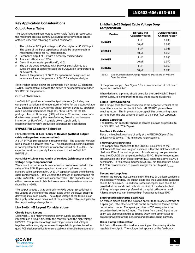
LinkSwitch-II Output Cable Voltage Drop Compensation
Device BYPASS Pin Capacitor Value
Output Voltage Change Factor
LNK6131 mF 1.035
10 mF 1.055
LNK6141 mF 1.045
10 mF 1.065
LNK6151 mF 1.050
10 mF 1.070
LNK6161 mF 1.060
10 mF 1.090
Table 2. Cable Compensation Change Factor vs. Device and BYPASS Pin Capacitor Value.
winding is a reflection of the secondary winding voltage while the internal MOSFET is off. Therefore any leakage inductance induced ringing can affect output regulation. Optimizing the drain clamp to minimize the high frequency ringing will give the best regulation. Figure 7 shows the desired drain voltage waveform compared to Figure 8 with a large undershoot due to the leakage inductance induced ring. This will reduce the output voltage regulation perfor- mance. To reduce this adjust the value of the resistor in series with the clamp diode.
Addition of a Bias Circuit for Higher Light Load Efficiency and Lower No-load Input Power Consumption.
The addition of a bias circuit can decrease the no-load input power from ~200 mW down to less than 30 mW at 230 VAC input. Light load efficiency also increases which may avoid the need to use a Schottky barrier vs PN junction output diode while still meeting average efficiency requirements.
The power supply schematic shown in Figure 5 has the bias circuit incorporated. Diode D6, C5 and R4 form the bias circuit. As the output voltage is less than 8 V, an additional transformer winding is needed, AC stacked on top of the feedback winding. This provides a high enough voltage to supply the BYPASS pin even during low switching frequency operation at no-load.
In Figure 5 the additional bias winding (from pin 2 to pin 1) is stacked on top of the feedback winding (pin 4 to pin 2). Diode D6 rectifies the output and C5 is the filter capacitor. A 10 uF capacitor is recommended to hold up the bias voltage at low switching frequencies. The capacitor type is not critical but the voltage rating should be above the maximum value of VBIAS. The recommended current into the BYPASS pin is equal to IC supply current (~0.5 mA) at the minimum bias winding voltage. The BYPASS pin current should not
Figure 6. PCB Layout Example Showing 5.1 W Design using P Package.
exceed 3 mA at the maximum bias winding voltage. The value of R4 is calculated according to (VBIAS – VBP)/IS2, where VBIAS (10 V typ.) is the voltage across C5, IS2 (0.5 mA typ.) is the IC supply current and VBP (6.0 V typ.) is the BYPASS pin voltage. The parameters IS2 and VBP are provided in the parameter table of the LinkSwitch-II data sheet. Diode D6 can be any low cost diode such as FR102, 1N4148 or BAV19/20/21.
Quick Design ChecklistAs with any power supply design, all LinkSwitch-II designs should be verified on the bench to make sure that component specifications are not exceeded under worst-case conditions. The following minimum set of tests is strongly recommended:
1. Maximum drain voltage – Verify that peak VDS does not exceed 680 V at the highest input voltage and maximum output power.
2. Maximum drain current – At maximum ambient temperature, maximum input voltage and maximum output load, verify drain current waveforms at start-up for any signs of transformer saturation and excessive leading edge current spikes. LinkSwitch-II has a leading edge blanking time of 170 ns to prevent premature termination of the ON-cycle.
3. Thermal check – At maximum output power, both minimum and maximum input voltage and maximum ambient temperature; verify that temperature specifications are not exceeded for LinkSwitch-II, transformer, output diodes and output capacitors. Enough thermal margin should be allowed for part-to-part variation of the RDS(ON) of LinkSwitch-II, as specified in the data sheet. To assure 10% CC tolerance a maximum SOURCE pin temperature of 90 ºC is recommended.
Design ToolsUp-to-date information on design tools can be found at the Power Integrations web site: www.power.com
SOURCE = 0 V; TJ = 0 to 100 °C (Unless Otherwise Specified)
Min Typ Max Units
Control Functions
Output Frequency fOSC
TJ = 25 °C, VFB = VFBth tON × IFB = 2 mA-ms
See Notes A, G
LNK603/6 59 66 73kHz
LNK613/6 58 65 72
Frequency Ratio (Constant Current) fRATIO(CC)
TJ = 25 °C Between VFB = 1.0 V and VFB = 1.6 V 1.59 1.635 1.68
Frequency Ratio (Inductance Correction) fRATIO(IC)
Between tON × IFB = 1.6 mA × ms and tON × IFB = 2 mA × ms 1.160 1.215 1.265
Frequency Jitter Peak-Peak Jitter Compared to Average Frequency, TJ = 25 °C ±7 %
Ratio of Output Fre- quency at Auto-Restart fOSC(AR)
TJ = 25 °C Relative to fOSC
12 16.5 21 %
Maximum Duty Cycle DCMAX See Notes D, E 55 %
FEEDBACK Pin Voltage VFBth
TJ = 25 °C CBP = 10 mFSee Note F
LNK603/604P 1.815 1.840 1.865
V
LNK603/604D 1.855 1.880 1.905
LNK605P, LNK605D 1.835 1.860 1.885
LNK606P/G/D 1.775 1.800 1.825
LNK613/614P 1.935 1.960 1.985
LNK613/614/615D 1.975 2.000 2.025
LNK615P 1.975 2.000 2.025
LNK616P/G/D 1.935 1.960 1.985
FEEDBACK Pin Voltage Temperature Coefficient TCVFB -0.01 %/°C
FEEDBACK Pin Voltage at Turn-OFF Threshold VFB(AR) 0.65 0.72 0.79 V
Cable Compensation Factor υFB LNK613
CBP = 1 mF 1.035
CBP = 10 mF 1.055
Absolute Maximum Ratings1,5
DRAIN Voltage ........................................................-0.3 V to 700 V DRAIN Peak Current: LNK603/613 .............................. 320 (480) mA4 LNK604/614 ..............................400 (600) mA4
LNK606/616 ..............................654 (980) mA4 Peak Negative Pulsed Drain Current ...................................-100 mA2 FEEDBACK Pin Voltage ................................................ -0.3 V to 9 V6 FEEDBACK Pin Current ........................................................100 mA BYPASS Pin Voltage ...................................................... -0.3 V to 9 VBYPASS Pin Current ...............................................................10 mA Storage Temperature ...................................... ..........-65 °C to 150 °COperating Junction Temperature ..............................-40 °C to 150 °C
Lead Temperature(3) .................................................................260 °C Notes: 1. All voltages referenced to SOURCE, TA = 25 °C. 2. Duration not to exceed 2 ms. 3. 1/16 in. from case for 5 seconds.4. The higher peak DRAIN current is allowed while the DRAIN voltage is simultaneously less than 400 V. 5. Maximum ratings specified may be applied, one at a time without causing permanent damage to the product. Exposure to Absolute Maximum ratings for extended periods of time may affect product reliability. 6. -1 V for current pulse ≤5 mA out of the pin and a duration of ≤500 ns.
Thermal Resistance
Thermal Resistance: P or G Package: (qJA) .......................... .............. 70 °C/W2; 60 °C/W3
Notes: 1. Measured on pin 8 (SOURCE) close to plastic interface. 2. Soldered to 0.36 sq. in. (232 mm2), 2 oz. (610 g/m2) copper clad. 3. Soldered to 1 sq. in. (645 mm2), 2 oz. (610 g/m2) copper clad.
SOURCE = 0 V; TJ = 0 to 100 °C (Unless Otherwise Specified)
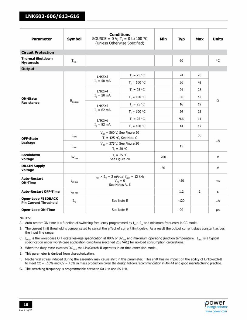
Min Typ Max Units
Circuit Protection
Thermal Shutdown Hysteresis TSDH 60 °C
Output
ON-State Resistance RDS(ON)
LNK6X3ID = 50 mA
TJ = 25 °C 24 28
W
TJ = 100 °C 36 42
LNK6X4ID = 50 mA
TJ = 25 °C 24 28
TJ = 100 °C 36 42
LNK6X5ID = 62 mA
TJ = 25 °C 16 19
TJ = 100 °C 24 28
LNK6X6ID = 82 mA
TJ = 25 °C 9.6 11
TJ = 100 °C 14 17
OFF-State Leakage
IDSS1
VDS = 560 V, See Figure 20
TJ = 125 °C, See Note C50
mA
IDSS2
VDS = 375 V, See Figure 20
TJ = 50 °C15
Breakdown Voltage BVDSS
TJ = 25 °C See Figure 20 700 V
DRAIN Supply Voltage 50 V
Auto-Restart ON-Time tAR-ON
tON × IFB = 2 mA-ms, fOSC = 12 kHz VFB = 0
See Notes A, E450 ms
Auto-Restart OFF-Time tAR-OFF 1.2 2 s
Open-Loop FEEDBACK Pin Current Threshold IOL See Note E -120 mA
Open-Loop ON-Time See Note E 90 ms
NOTES:A. Auto-restart ON-time is a function of switching frequency programmed by ton× IFB and minimum frequency in CC mode.
B. The current limit threshold is compensated to cancel the effect of current limit delay. As a result the output current stays constant across the input line range.
C. IDSS1 is the worst-case OFF-state leakage specification at 80% of BVDSS and maximum operating junction temperature. IDSS2 is a typical specification under worst-case application conditions (rectified 265 VAC) for no-load consumption calculations.
D. When the duty-cycle exceeds DCMAX the LinkSwitch-II operates in on-time extension mode.
E. This parameter is derived from characterization.
F. Mechanical stress induced during the assembly may cause shift in this parameter. This shift has no impact on the ability of LinkSwitch-II to meet CC = ±10% and CV = ±5% in mass production given the design follows recommendation in AN-44 and good manufacturing practice.
G. The switching frequency is programmable between 60 kHz and 85 kHz.
Figure 20. Test Set-up for Leakage and Breakdown Tests.
PI-4962-012915
16 V
To measure BVDSS, IDSS1, and IDSS2 follow these steps:1) Close S1, open S2.2) Power-up VIN source (16 V).3) Open S1, close S2.4) Measure I/V characteristics of DRAIN pin using the curve tracer.
.1 µF
1 µF
VIN
LinkSwitch-II
5 µF 50 kΩ
+
CurveTracer
S1 S24 kΩ
10 kΩ
S
D S
S
FB
SBP/M
Figure 21. Test Set-up for Output Current Measurements.
PI-4963-012315
50 V
1) The transformer inductance is chosen to set the value of tON × IFB to 2 mA × µS.2) RO is chosen to operate test circuit in the CC region.3) VO is measured.4) Output current is VO / RO.
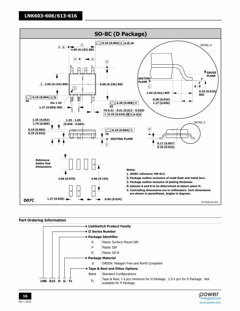
Notes:1. Package dimensions conform to JEDEC specification MS-001-AB (Issue B 7/85) for standard dual-in-line (DIP) package with .300 inch row spacing.2. Controlling dimensions are inches. Millimeter sizes are shown in parentheses.3. Dimensions shown do not include mold flash or other protrusions. Mold flash or protrusions shall not exceed .006 (.15) on any side.4. Pin locations start with Pin 1, and continue counter-clock-wise to Pin 8 when viewed from the top. The notch and/or dimple are aids in locating Pin 1. Pin 3 is omitted.5. Minimum metal to metal spacing at the package body for the omitted lead location is .137 inch (3.48 mm).6. Lead width measured at package body. 7. Lead spacing measured with the leads constrained to be perpendicular to plane T.
Notes:1. Controlling dimensions are inches. Millimeter sizes are shown in parentheses.2. Dimensions shown do not include mold flash or other protrusions. Mold flash or protrusions shall not exceed .006 (.15) on any side.3. Pin locations start with Pin 1, and continue counter-clock- wise to Pin 8 when viewed from the top. Pin 3 is omitted.4. Minimum metal to metal spacing at the package body for the omitted lead location is .137 inch (3.48 mm).5. Lead width measured at package body. 6. D and E are referenced datums on the package body.
TL Tape & Reel, 1 k pcs minimum for G Package. 2.5 k pcs for D Package. Not available for P Package.LNK 615 D G - TL
PI-4526-012315D07C
3.90 (0.154) BSC
Notes:1. JEDEC reference: MS-012.2. Package outline exclusive of mold flash and metal burr.3. Package outline inclusive of plating thickness.4. Datums A and B to be determined at datum plane H.5. Controlling dimensions are in millimeters. Inch dimensions are shown in parenthesis. Angles in degrees.
For the latest updates, visit our website: www.power.comPower Integrations reserves the right to make changes to its products at any time to improve reliability or manufacturability. Power Integrations does not assume any liability arising from the use of any device or circuit described herein. POWER INTEGRATIONS MAKES NO WARRANTY HEREIN AND SPECIFICALLY DISCLAIMS ALL WARRANTIES INCLUDING, WITHOUT LIMITATION, THE IMPLIED WARRANTIES OF MERCHANTABILITY, FITNESS FOR A PARTICULAR PURPOSE, AND NON-INFRINGEMENT OF THIRD PARTY RIGHTS.
Patent InformationThe products and applications illustrated herein (including transformer construction and circuits external to the products) may be covered by one or more U.S. and foreign patents, or potentially by pending U.S. and foreign patent applications assigned to Power Integrations. A complete list of Power Integrations patents may be found at www.power.com. Power Integrations grants its customers a license under certain patent rights as set forth at www.power.com/ip.htm.
Life Support PolicyPOWER INTEGRATIONS PRODUCTS ARE NOT AUTHORIZED FOR USE AS CRITICAL COMPONENTS IN LIFE SUPPORT DEVICES OR SYSTEMS WITHOUT THE EXPRESS WRITTEN APPROVAL OF THE PRESIDENT OF POWER INTEGRATIONS. As used herein:
1. A Life support device or system is one which, (i) is intended for surgical implant into the body, or (ii) supports or sustains life, and (iii) whose failure to perform, when properly used in accordance with instructions for use, can be reasonably expected to result in significant injury or death to the user.
2. A critical component is any component of a life support device or system whose failure to perform can be reasonably expected to cause the failure of the life support device or system, or to affect its safety or effectiveness.