rXXXX American Chemical Society A dx.doi.org/10.1021/nl1042648 | Nano Lett. XXXX, XXX, 000–000 LETTER pubs.acs.org/NanoLett Localized States and Resultant Band Bending in Graphene Antidot Superlattices Milan Begliarbekov, † Onejae Sul, ‡ John Santanello, † Nan Ai, † Xi Zhang, † Eui-Hyeok Yang, ‡ and Stefan Strauf* ,† † Department of Physics and Engineering Physics and ‡ Department of Mechanical Engineering, Stevens Institute of Technology, Hoboken, New Jersey 07030, United States b S Supporting Information Graphene, a two-dimensional monolayer of carbon atoms arranged in a hexagonal lattice, has been recently isolated 1 and shown to exhibit excellent electrical, 2,3 thermal, 4 mechanical, 5 and optical 6 properties. Electron transport has been studied exten- sively in single- and few-layer graphene sheets, 7,8 while optoelec- tronic properties and light-matter interaction in nanostructured graphene gain increasingly more interest in the research commu- nity, in particular since the advent of first ultrafast graphene photodetectors. 9 Single layer graphene absorbs only 2.3% of the incident radiation in the visible spectrum; 10 consequently, effi- cient photocarrier separation within graphene becomes particu- larly important. In order to create a built-in electrical field that facilitates carrier separation, silicon based technology relies on the pn-junction that is created by doping the silicon lattice. Physical doping of graphene has been previously achieved by addition of extrinsic atomic 11,12 or molecular 13,14 species either by adsorption or intercalation into the graphene lattice. 12,15 A potentially simpler way to make graphene a viable material for optoelec- tronics can be achieved by utilizing lateral electric fields created by Schottky barriers near the source and drain metal contacts, 9,16,17 as was previously done in carbon nanotubes. 18 In the presence of such metal contacts it was also observed that nanotube fluores- cence can be significantly enhanced. 19 While graphene does not display any exciton emission, quantum dots placed on unpat- terned graphene were recently shown to undergo strong fluores- cence quenching, which is indicative of energy transfer from the quantum dot exciton oscillator into graphene. 20 Such hybrids between graphene and light harvesting molecules can potentially overcome the low absorption efficiency of bare graphene. Nanostructured graphene offers further possibilities to explore light harvesting and carrier separation. Of particular interest are the so-called antidot superlattices, i.e., lattices comprised of a periodic arrangement of perforations in the underlying graphene structure. These superlattices were predicted to possess a non- negligible magnetic moment, 21 a small band gap 22-25 that can be controlled by the antidot filling fraction, 26,27 and Peierls type electron-hole coupling that leads to polaronic behavior. 26 In a previous work, Heydrich et al., showed that the introduction of an antidot superlattice results in the stiffening of the G band in graphene’s Raman spectrum, as well as an energetic shift of the G and G 0 bands commensurate with p-type doping. 28 Furthermore, recent theoretical predictions show that the periphery of gra- phene possesses a nonnegligible density of states N edge that is spatially localized at the edges and is distinct from the bulk states N bulk that are present in graphene’s interior regions. Conse- quently, antidot superlattices provide a natural framework for studying these states and their properties, since the edge states in these systems coexist with the bulk states, unlike in dot lattices, where the ratio of edge to bulk states is small. Here we report an electro-optical study of dye sensitized graphene antidot superlattices with the purpose of elucidating the role of the localized edge state density on its light-harvesting properties. The amount of p-type doping introduced by the edge states is quantified for various antidot filling fractions using confocal μ-Raman spectroscopy and transport measurements. We show that the fluorescence from deposited dye molecules strongly quenches in linear proportion to the antidot filling fraction, whereas it was enhanced in the presence of free carriers in unpatterned but electrically backgated samples. This contrast- ing behavior is strongly indicative of a built-in lateral electric field that accounts for fluorescence quenching as well as p-type doping Received: December 7, 2010 Revised: January 20, 2011 ABSTRACT: We fabricated dye sensitized graphene antidot superlattices with the purpose of elucidating the role of the localized edge state density. The fluorescence from deposited dye molecules was found to strongly quench as a function of increasing antidot filling fraction, whereas it was enhanced in unpatterned but electrically backgated samples. This contrast- ing behavior is strongly indicative of a built-in lateral electric field that accounts for fluorescence quenching as well as p-type doping. These findings are of great interest for light-harvesting applications that require field separation of electron-hole pairs. KEYWORDS: Antidot, graphene superlattice, band bending
Transcript
rXXXX American Chemical Society A dx.doi.org/10.1021/nl1042648 |Nano Lett. XXXX, XXX, 000–000
LETTER
pubs.acs.org/NanoLett
Localized States and Resultant Band Bending in Graphene AntidotSuperlatticesMilan Begliarbekov,† Onejae Sul,‡ John Santanello,† Nan Ai,† Xi Zhang,† Eui-Hyeok Yang,‡ andStefan Strauf*,†
†Department of Physics and Engineering Physics and ‡Department of Mechanical Engineering, Stevens Institute of Technology,Hoboken, New Jersey 07030, United States
bS Supporting Information
Graphene, a two-dimensional monolayer of carbon atomsarranged in a hexagonal lattice, has been recently isolated1 andshown to exhibit excellent electrical,2,3 thermal,4 mechanical,5 andoptical6 properties. Electron transport has been studied exten-sively in single- and few-layer graphene sheets,7,8 while optoelec-tronic properties and light-matter interaction in nanostructuredgraphene gain increasingly more interest in the research commu-nity, in particular since the advent of first ultrafast graphenephotodetectors.9 Single layer graphene absorbs only 2.3% of theincident radiation in the visible spectrum;10 consequently, effi-cient photocarrier separation within graphene becomes particu-larly important. In order to create a built-in electrical field thatfacilitates carrier separation, silicon based technology relies on thepn-junction that is created by doping the silicon lattice. Physicaldoping of graphene has been previously achieved by addition ofextrinsic atomic11,12 ormolecular13,14 species either by adsorptionor intercalation into the graphene lattice.12,15 A potentiallysimpler way to make graphene a viable material for optoelec-tronics can be achieved by utilizing lateral electric fields created bySchottky barriers near the source and drain metal contacts,9,16,17
as was previously done in carbon nanotubes.18 In the presence ofsuch metal contacts it was also observed that nanotube fluores-cence can be significantly enhanced.19 While graphene does notdisplay any exciton emission, quantum dots placed on unpat-terned graphene were recently shown to undergo strong fluores-cence quenching, which is indicative of energy transfer from thequantum dot exciton oscillator into graphene.20 Such hybridsbetween graphene and light harvesting molecules can potentiallyovercome the low absorption efficiency of bare graphene.
Nanostructured graphene offers further possibilities to explorelight harvesting and carrier separation. Of particular interest arethe so-called antidot superlattices, i.e., lattices comprised of a
periodic arrangement of perforations in the underlying graphenestructure. These superlattices were predicted to possess a non-negligible magnetic moment,21 a small band gap22-25 that can becontrolled by the antidot filling fraction,26,27 and Peierls typeelectron-hole coupling that leads to polaronic behavior.26 In aprevious work, Heydrich et al., showed that the introduction ofan antidot superlattice results in the stiffening of the G band ingraphene’s Raman spectrum, as well as an energetic shift of the Gand G0 bands commensurate with p-type doping.28 Furthermore,recent theoretical predictions show that the periphery of gra-phene possesses a nonnegligible density of states Nedge that isspatially localized at the edges and is distinct from the bulk statesNbulk that are present in graphene’s interior regions. Conse-quently, antidot superlattices provide a natural framework forstudying these states and their properties, since the edge states inthese systems coexist with the bulk states, unlike in dot lattices,where the ratio of edge to bulk states is small.
Here we report an electro-optical study of dye sensitizedgraphene antidot superlattices with the purpose of elucidatingthe role of the localized edge state density on its light-harvestingproperties. The amount of p-type doping introduced by the edgestates is quantified for various antidot filling fractions usingconfocal μ-Raman spectroscopy and transport measurements.We show that the fluorescence from deposited dye moleculesstrongly quenches in linear proportion to the antidot fillingfraction, whereas it was enhanced in the presence of free carriersin unpatterned but electrically backgated samples. This contrast-ing behavior is strongly indicative of a built-in lateral electric fieldthat accounts for fluorescence quenching as well as p-type doping
Received: December 7, 2010Revised: January 20, 2011
ABSTRACT: We fabricated dye sensitized graphene antidotsuperlattices with the purpose of elucidating the role of thelocalized edge state density. The fluorescence from depositeddye molecules was found to strongly quench as a function ofincreasing antidot filling fraction, whereas it was enhanced inunpatterned but electrically backgated samples. This contrast-ing behavior is strongly indicative of a built-in lateral electricfield that accounts for fluorescence quenching as well as p-typedoping. These findings are of great interest for light-harvesting applications that require field separation of electron-hole pairs.
KEYWORDS: Antidot, graphene superlattice, band bending
B dx.doi.org/10.1021/nl1042648 |Nano Lett. XXXX, XXX, 000–000
Nano Letters LETTER
and the observed Raman signatures. Our study provides newinsights into the interplay of localized edge states in antidotlattices and the resulting band bending, which are critical proper-ties to enable novel applications of nanostructured graphene forlight harvesting and photovoltaic devices.Results and Discussion. Antidot Superlattices. Graphene
flakes used in these experiments were prepared by micromecha-nical exfoliation of natural graphite onto a degenerately doped pþþ
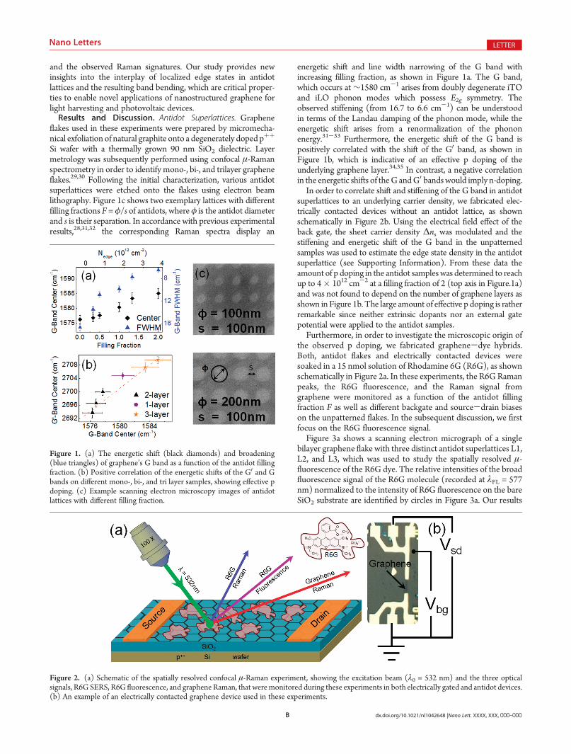
Si wafer with a thermally grown 90 nm SiO2 dielectric. Layermetrology was subsequently performed using confocal μ-Ramanspectrometry in order to identify mono-, bi-, and trilayer grapheneflakes.29,30 Following the initial characterization, various antidotsuperlattices were etched onto the flakes using electron beamlithography. Figure 1c shows two exemplary lattices with differentfilling fractions F = φ/s of antidots, where φ is the antidot diameterand s is their separation. In accordance with previous experimentalresults,28,31,32 the corresponding Raman spectra display an
energetic shift and line width narrowing of the G band withincreasing filling fraction, as shown in Figure 1a. The G band,which occurs at∼1580 cm-1 arises from doubly degenerate iTOand iLO phonon modes which possess E2g symmetry. Theobserved stiffening (from 16.7 to 6.6 cm-1) can be understoodin terms of the Landau damping of the phonon mode, while theenergetic shift arises from a renormalization of the phononenergy.31-33 Furthermore, the energetic shift of the G band ispositively correlated with the shift of the G0 band, as shown inFigure 1b, which is indicative of an effective p doping of theunderlying graphene layer.34,35 In contrast, a negative correlationin the energetic shifts of theG andG0 bandswould imply n-doping.In order to correlate shift and stiffening of the G band in antidot
superlattices to an underlying carrier density, we fabricated elec-trically contacted devices without an antidot lattice, as shownschematically in Figure 2b. Using the electrical field effect of theback gate, the sheet carrier density Δns was modulated and thestiffening and energetic shift of the G band in the unpatternedsamples was used to estimate the edge state density in the antidotsuperlattice (see Supporting Information). From these data theamount of p doping in the antidot samples was determined to reachup to 4� 1012 cm-2 at a filling fraction of 2 (top axis in Figure.1a)and was not found to depend on the number of graphene layers asshown in Figure 1b. The large amount of effective p doping is ratherremarkable since neither extrinsic dopants nor an external gatepotential were applied to the antidot samples.Furthermore, in order to investigate the microscopic origin of
the observed p doping, we fabricated graphene-dye hybrids.Both, antidot flakes and electrically contacted devices weresoaked in a 15 nmol solution of Rhodamine 6G (R6G), as shownschematically in Figure 2a. In these experiments, the R6G Ramanpeaks, the R6G fluorescence, and the Raman signal fromgraphene were monitored as a function of the antidot fillingfraction F as well as different backgate and source-drain biaseson the unpatterned flakes. In the subsequent discussion, we firstfocus on the R6G fluorescence signal.Figure 3a shows a scanning electron micrograph of a single
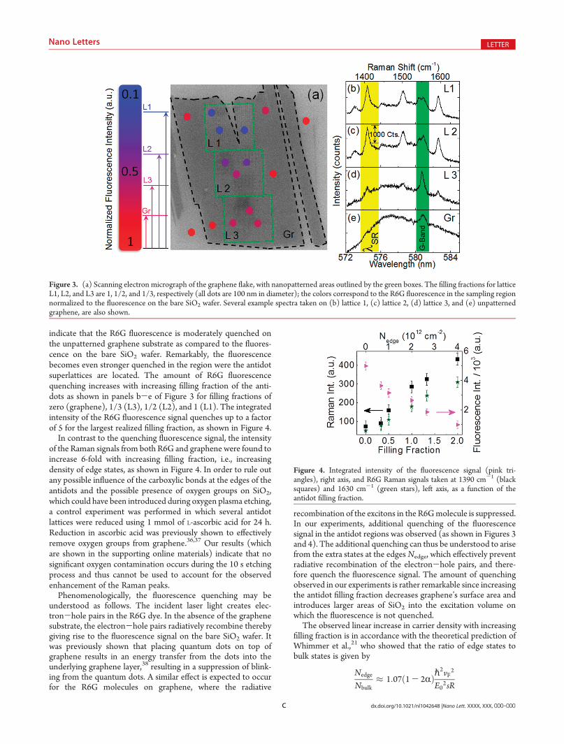
bilayer graphene flake with three distinct antidot superlattices L1,L2, and L3, which was used to study the spatially resolved μ-fluorescence of the R6G dye. The relative intensities of the broadfluorescence signal of the R6G molecule (recorded at λFL = 577nm) normalized to the intensity of R6G fluorescence on the bareSiO2 substrate are identified by circles in Figure 3a. Our results
Figure 1. (a) The energetic shift (black diamonds) and broadening(blue triangles) of graphene’s G band as a function of the antidot fillingfraction. (b) Positive correlation of the energetic shifts of the G0 and Gbands on different mono-, bi-, and tri layer samples, showing effective pdoping. (c) Example scanning electron microscopy images of antidotlattices with different filling fraction.
Figure 2. (a) Schematic of the spatially resolved confocal μ-Raman experiment, showing the excitation beam (λ0 = 532 nm) and the three opticalsignals, R6G SERS, R6G fluorescence, and graphene Raman, that weremonitored during these experiments in both electrically gated and antidot devices.(b) An example of an electrically contacted graphene device used in these experiments.
C dx.doi.org/10.1021/nl1042648 |Nano Lett. XXXX, XXX, 000–000
Nano Letters LETTER
indicate that the R6G fluorescence is moderately quenched onthe unpatterned graphene substrate as compared to the fluores-cence on the bare SiO2 wafer. Remarkably, the fluorescencebecomes even stronger quenched in the region were the antidotsuperlattices are located. The amount of R6G fluorescencequenching increases with increasing filling fraction of the anti-dots as shown in panels b-e of Figure 3 for filling fractions ofzero (graphene), 1/3 (L3), 1/2 (L2), and 1 (L1). The integratedintensity of the R6G fluorescence signal quenches up to a factorof 5 for the largest realized filling fraction, as shown in Figure 4.In contrast to the quenching fluorescence signal, the intensity
of the Raman signals from both R6G and graphene were found toincrease 6-fold with increasing filling fraction, i.e., increasingdensity of edge states, as shown in Figure 4. In order to rule outany possible influence of the carboxylic bonds at the edges of theantidots and the possible presence of oxygen groups on SiO2,which could have been introduced during oxygen plasma etching,a control experiment was performed in which several antidotlattices were reduced using 1 mmol of L-ascorbic acid for 24 h.Reduction in ascorbic acid was previously shown to effectivelyremove oxygen groups from graphene.36,37 Our results (whichare shown in the supporting online materials) indicate that nosignificant oxygen contamination occurs during the 10 s etchingprocess and thus cannot be used to account for the observedenhancement of the Raman peaks.Phenomenologically, the fluorescence quenching may be
understood as follows. The incident laser light creates elec-tron-hole pairs in the R6G dye. In the absence of the graphenesubstrate, the electron-hole pairs radiatively recombine therebygiving rise to the fluorescence signal on the bare SiO2 wafer. Itwas previously shown that placing quantum dots on top ofgraphene results in an energy transfer from the dots into theunderlying graphene layer,38 resulting in a suppression of blink-ing from the quantum dots. A similar effect is expected to occurfor the R6G molecules on graphene, where the radiative
recombination of the excitons in the R6Gmolecule is suppressed.In our experiments, additional quenching of the fluorescencesignal in the antidot regions was observed (as shown in Figures 3and 4). The additional quenching can thus be understood to arisefrom the extra states at the edges Nedge, which effectively preventradiative recombination of the electron-hole pairs, and there-fore quench the fluorescence signal. The amount of quenchingobserved in our experiments is rather remarkable since increasingthe antidot filling fraction decreases graphene’s surface area andintroduces larger areas of SiO2 into the excitation volume onwhich the fluorescence is not quenched.The observed linear increase in carrier density with increasing
filling fraction is in accordance with the theoretical prediction ofWhimmer et al.,21 who showed that the ratio of edge states tobulk states is given by
Nedge
Nbulk� 1:07ð1- 2RÞp
2vF2
E02sR
Figure 3. (a) Scanning electron micrograph of the graphene flake, with nanopatterned areas outlined by the green boxes. The filling fractions for latticeL1, L2, and L3 are 1, 1/2, and 1/3, respectively (all dots are 100 nm in diameter); the colors correspond to the R6G fluorescence in the sampling regionnormalized to the fluorescence on the bare SiO2 wafer. Several example spectra taken on (b) lattice 1, (c) lattice 2, (d) lattice 3, and (e) unpatternedgraphene, are also shown.
Figure 4. Integrated intensity of the fluorescence signal (pink tri-angles), right axis, and R6G Raman signals taken at 1390 cm-1 (blacksquares) and 1630 cm-1 (green stars), left axis, as a function of theantidot filling fraction.
D dx.doi.org/10.1021/nl1042648 |Nano Lett. XXXX, XXX, 000–000
Nano Letters LETTER
where p is the reduced Planck’s constant, vF is the Fermi velocityin graphene, R is a parameter that characterizes edge roughness,E0 is the energy width of the band of edge states, s is the antidotseparation, and R is the antidot radius. Therefore, decreasing s oralternatively increasing R gives rise to a linear increase in Nedge.Gate-Tunable Fluorescence. In order to further elucidate the
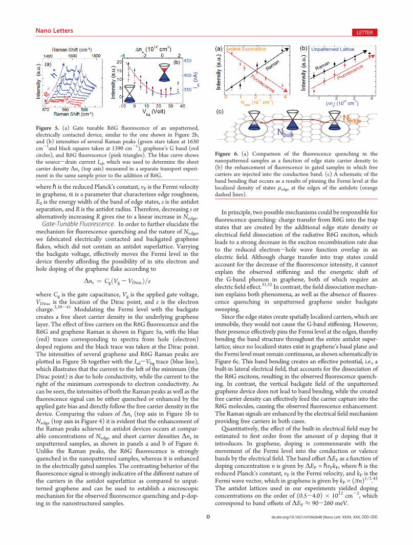
mechanism for fluorescence quenching and the nature of Nedge,we fabricated electrically contacted and backgated grapheneflakes, which did not contain an antidot superlattice. Varryingthe backgate voltage, effectively moves the Fermi level in thedevice thereby affording the possibility of in situ electron andhole doping of the graphene flake according to
Δns ¼ CgðVg - VDiracÞ=ewhere Cg is the gate capacitance, Vg is the applied gate voltage,VDirac is the location of the Dirac point, and e is the electroncharge.3,39-41 Modulating the Fermi level with the backgatecreates a free sheet carrier density in the underlying graphenelayer. The effect of free carriers on the R6G fluorescence and theR6G and graphene Raman is shown in Figure 5a, with the blue(red) traces corresponding to spectra from hole (electron)doped regions and the black trace was taken at the Dirac point.The intensities of several graphene and R6G Raman peaks areplotted in Figure 5b together with the Isd-Vbg trace (blue line),which illustrates that the current to the left of the minimum (theDirac point) is due to hole conductivity, while the current to theright of the minimum corresponds to electron conductivity. Ascan be seen, the intensities of both the Raman peaks as well as thefluorescence signal can be either quenched or enhanced by theapplied gate bias and directly follow the free carrier density in thedevice. Comparing the values of Δns (top axis in Figure 5b toNedge (top axis in Figure 4) it is evident that the enhancement ofthe Raman peaks achieved in antidot devices occurs at compar-able concentrations of Nedge and sheet carrier densities Δns inunpatterned samples, as shown in panels a and b of Figure 6.Unlike the Raman peaks, the R6G fluorescence is stronglyquenched in the nanopatterned samples, whereas it is enhancedin the electrically gated samples. The contrasting behavior of thefluorescence signal is strongly indicative of the different nature ofthe carriers in the antidot superlattice as compared to unpat-terned graphene and can be used to establish a microscopicmechanism for the observed fluorescence quenching and p-dop-ing in the nanostructured samples.
In principle, two possible mechanisms could be responsible forfluorescence quenching: charge transfer from R6G into the trapstates that are created by the additional edge state density orelectrical field dissociation of the radiative R6G exciton, whichleads to a strong decrease in the exciton recombination rate dueto the reduced electron-hole wave function overlap in anelectric field. Although charge transfer into trap states couldaccount for the decrease of the fluorescence intensity, it cannotexplain the observed stiffening and the energetic shift ofthe G-band phonon in graphene, both of which require anelectric field effect.31,32 In contrast, the field dissociationmechan-ism explains both phenomena, as well as the absence of fluores-cence quenching in unpatterned graphene under backgatesweeping.Since the edge states create spatially localized carriers, which are
immobile, they would not cause the G-band stiffening. However,their presence effectively pins the Fermi level at the edges, therebybending the band structure throughout the entire antidot super-lattice, since no localized states exist in graphene’s basal plane andthe Fermi levelmust remain continuous, as shown schematically inFigure 6c. This band bending creates an effective potential, i.e., abuilt-in lateral electrical field, that accounts for the dissociation ofthe R6G excitons, resulting in the observed fluorescence quench-ing. In contrast, the vertical backgate field of the unpatternedgraphene device does not lead to band bending, while the createdfree carrier density can effectively feed the carrier capture into theR6G molecules, causing the observed fluorescence enhancement.The Raman signals are enhanced by the electrical field mechanismproviding free carriers in both cases.Quantitatively, the effect of the built-in electrical field may be
estimated to first order from the amount of p doping that itintroduces. In graphene, doping is commensurate with themovement of the Fermi level into the conduction or valencebands by the electrical field. The band offsetΔEF as a function ofdoping concentration n is given by ΔEF = pvFkF, where p is thereduced Planck’s constant, vF is the Fermi velocity, and kF is theFermi wave vector, which in graphene is given by kF = (πn)
1/2.42
The antidot lattices used in our experiments yielded dopingconcentrations on the order of (0.5-4.0) � 1012 cm-2, whichcorrespond to band offsets of ΔEF ≈ 90-260 meV.
Figure 5. (a) Gate tunable R6G fluorescence of an unpatterned,electrically contacted device, similar to the one shown in Figure 2b,and (b) intensities of several Raman peaks (green stars taken at 1630cm-1and black squares taken at 1390 cm-1), graphene’s G band (redcircles), and R6G fluorescence (pink triangles). The blue curve showsthe source-drain current Isd, which was used to determine the sheetcarrier density Δns (top axis) measured in a separate transport experi-ment in the same sample prior to the addition of R6G.
Figure 6. (a) Comparison of the fluorescence quenching in thenanopatterned samples as a function of edge state carrier density to(b) the enhancement of fluorescence in gated samples in which freecarriers are injected into the conduction band. (c) A schematic of theband bending that occurs as a results of pinning the Fermi level at thelocalized density of states Fedge at the edges of the antidots (orangedashed lines).
E dx.doi.org/10.1021/nl1042648 |Nano Lett. XXXX, XXX, 000–000
Nano Letters LETTER
The Fermi level pinning at the localized carrier density in theantidot superlattice is similar to Fermi level pinning of a Schottkybarrier at an graphene-metal interface that is used to separatephotogenerated carriers in optoelectronic devices based, forexample, on carbon nanotubes.9,16,18 In our case, however, nometal was deposited onto graphene and the pinning occurs at thelocalized edge states that are a direct consequence of the antidotsuperlattice.In summary, we fabricated several graphene antidot super-
lattices usingmono-, bi-, and trilayer flakes and observed effectivep-type doping which increases with larger filling fractions, asevident from their Raman signatures. We furthermore showedthat after depositing R6G dye on these flakes, the correspondingfluorescence signal is strongly quenched with increasing antidotfilling fraction, while the Raman signal is enhanced. These resultsare indicative to a microscopic mechanism in which the Fermilevel becomes pinned at the antidot periphery giving rise to abuilt-in electric field, which accounts for the fluorescencequenching and the observed p-type doping in nanopatternedgraphene. These findings make antidot lattices of great interestfor carbon-based optoelectronics andmight be particularly usefulfor light-harvesting applications such as photodetectors and solarcells requiring efficient field separation of electron-hole pairs.
’ASSOCIATED CONTENT
bS Supporting Information. Sample preparation and charac-terization, estimation of the effective p-doping concentration, andestimating the effect of possible oxygen contamination. Thismaterialis available free of charge via the Internet at http://pubs.acs.org.
We are grateful to Francisco Guinea, Christopher Search,Svetlana Sukhishvili, and Henry Du for helpful discussions.Partial financial support was provided by by AFOSR, AwardNo. FA9550-08-1-013. We also thank the Center for FunctionalNanomaterials of the BrookhavenNational Laboratory, ContractDE-AC02-98CH10886, for the use of their clean rooms.
’REFERENCES
(1) Novoselov, K. S.; Geim, A. K.; Morozov, S. V.; Jiang, D.; Zhang,Y.; Dubonos, S. V.; Grigorieva, I. V.; Firsov, A. A. Science 2004,306, 666–669.(2) Lin, Y. M.; Dimitrakopoulos, C.; Jenkins, K. A.; Farmer, D. B.;
Chiu, H. Y.; Grill, A.; Avouris, P. Science 2010, 327, 662.(3) Bolotin, K. I.; Sikes, K. J.; Jiang, Z.; Klima, M.; Fudenberg, G.;
Hone, J.; Kim, P.; Stormer, H. L. Solid State Commun. 2008,146, 351–355.(4) Balandin, A. A.; Ghosh, S.; Bao,W.; Calizo, I.; Teweldebrhan, D.;
Miao, F.; Lau, C. N. Nano Lett. 2008, 8, 902–907.(5) Lee, C.; Wei, X.; Kysar, J. W.; Hone, J. Science 2008,
321, 385–388.(6) Bonaccorso, F.; Sun, Z.; Hasan, T.; Ferrari, A. C. Nat. Photonics
2010, 4, 611.(7) Novoselov, K. S.; Morozov, S. V.; Mohinddin, T. M. G.;
Ponomarenko, L. A.; Elias, D. C.; Yang, R.; Barbolina, I. I.; Blake, P.;Booth, T. J.; Jiang, D.; Giesbers, J.; Hill, E. W.; Geim, A. K. Phys. StatusSolidi B 2007, 244, 4106–4111.
(8) Neto, A. C.; Guinea, F.; Peres, N.; Novoselov, K.; Geim, A. Rev.Mod. Phys 2009, 81, 109–162.


![Synthesis of Layered Carbonitrides from Biotic Molecules ...download.xuebalib.com/xuebalib.com.31128.pdf · the primordial soup.[26,27] We are therefore interested and encouraged](https://static.documents.pub/doc/80x56/60c0e3c294bafc011c4e7d07/synthesis-of-layered-carbonitrides-from-biotic-molecules-the-primordial-soup2627.jpg)


