Top » Electronic Tutorials » Digital Theory - Table Of Contents » Chapter 3 - Logic Gates Categories DC Theory AC Theory Semiconductor Theory Digital Theory Experiments Datasheets Message Board Visit Our Store Assortment Kits Capacitors Crystal Oscillators Diodes Electron Tubes Heat Shrink Inductors Integrated Circuits (IC's) Light Emitting Diodes (LED's) Miscellaneous Motors Resistors Sockets Speakers Switches Terminal Blocks & Strips Test Equipment Transformers Transistors Sponsored Links Chapter 3: LOGIC GATES Digital signals and gates While the binary numeration system is an interesting mathematical abstraction, we haven't yet seen its practical application to electronics. This chapter is devoted to just that: practically applying the concept of binary bits to circuits. What makes binary numeration so important to the application of digital electronics is the ease in which bits may be represented in physical terms. Because a binary bit can only have one of two different values, either 0 or 1, any physical medium capable of switching between two saturated states may be used to represent a bit. Consequently, any physical system capable of representing binary bits is able to represent numerical quantities, and potentially has the ability to manipulate those numbers. This is the basic concept underlying digital computing. Electronic circuits are physical systems that lend themselves well to the representation of binary numbers. Transistors, when operated at their bias limits, may be in one of two different states: either cutoff (no controlled current) or saturation (maximum controlled current). If a transistor circuit is designed to maximize the probability of falling into either one of these states (and not operating in the linear, or active, mode), it can serve as a physical representation of a binary bit. A voltage signal measured at the output of such a circuit may also serve as a representation of a single bit, a low voltage representing a binary "0" and a (relatively) high voltage representing a binary "1." Note the following transistor circuit: In this circuit, the transistor is in a state of saturation by virtue of the applied input voltage (5 volts) through the two-position switch. Because it's saturated, the transistor drops very little voltage between collector and emitter, resulting in an output voltage of (practically) 0 volts. If we were using this circuit to represent binary bits, we would say that the input signal is a binary "1" and that the output signal is a binary "0." Any voltage close to full supply voltage (measured in reference to ground, of course) is considered a "1" and a lack of voltage is considered a "0." Alternative terms for these voltage levels are high (same as a binary "1") and low (same as a binary "0"). A general term for the representation of a binary bit by a circuit voltage is logic level . Moving the switch to the other position, we apply a binary "0" to the input and receive a binary "1" at the output: Related Sites None Logic Gates - Basic Electronic Tutorials http://www.opamp-electronics.com/tutorials/digital_theory_ch_003.htm 1 of 59 20/02/2012 08:52 PM
Transcript
Top » Electronic Tutorials » Digital Theory - Table Of Contents » Chapter 3 - Logic Gates
Categories
DC TheoryAC TheorySemiconductor TheoryDigital TheoryExperimentsDatasheetsMessage Board
Digital signals and gatesWhile the binary numeration system is an interesting mathematical abstraction, we haven't yet seenits practical application to electronics. This chapter is devoted to just that: practically applying theconcept of binary bits to circuits. What makes binary numeration so important to the application ofdigital electronics is the ease in which bits may be represented in physical terms. Because a binarybit can only have one of two different values, either 0 or 1, any physical medium capable ofswitching between two saturated states may be used to represent a bit. Consequently, any physicalsystem capable of representing binary bits is able to represent numerical quantities, and potentiallyhas the ability to manipulate those numbers. This is the basic concept underlying digital computing.
Electronic circuits are physical systems that lend themselves well to the representation of binarynumbers. Transistors, when operated at their bias limits, may be in one of two different states:either cutoff (no controlled current) or saturation (maximum controlled current). If a transistor circuitis designed to maximize the probability of falling into either one of these states (and not operating inthe linear, or active, mode), it can serve as a physical representation of a binary bit. A voltage signalmeasured at the output of such a circuit may also serve as a representation of a single bit, a lowvoltage representing a binary "0" and a (relatively) high voltage representing a binary "1." Note thefollowing transistor circuit:
In this circuit, the transistor is in a state of saturation by virtue of the applied input voltage (5 volts)through the two-position switch. Because it's saturated, the transistor drops very little voltagebetween collector and emitter, resulting in an output voltage of (practically) 0 volts. If we were usingthis circuit to represent binary bits, we would say that the input signal is a binary "1" and that theoutput signal is a binary "0." Any voltage close to full supply voltage (measured in reference toground, of course) is considered a "1" and a lack of voltage is considered a "0." Alternative termsfor these voltage levels are high (same as a binary "1") and low (same as a binary "0"). A generalterm for the representation of a binary bit by a circuit voltage is logic level.
Moving the switch to the other position, we apply a binary "0" to the input and receive a binary "1" atthe output:
What we've created here with a single transistor is a circuit generally known as a logic gate, orsimply gate. A gate is a special type of amplifier circuit designed to accept and generate voltagesignals corresponding to binary 1's and 0's. As such, gates are not intended to be used foramplifying analog signals (voltage signals between 0 and full voltage). Used together, multiple gatesmay be applied to the task of binary number storage (memory circuits) or manipulation (computingcircuits), each gate's output representing one bit of a multi-bit binary number. Just how this is doneis a subject for a later chapter. Right now it is important to focus on the operation of individual gates.
The gate shown here with the single transistor is known as an inverter, or NOT gate, because itoutputs the exact opposite digital signal as what is input. For convenience, gate circuits aregenerally represented by their own symbols rather than by their constituent transistors and resistors.The following is the symbol for an inverter:
An alternative symbol for an inverter is shown here:
Notice the triangular shape of the gate symbol, much like that of an operational amplifier. As wasstated before, gate circuits actually are amplifiers. The small circle, or "bubble" shown on either theinput or output terminal is standard for representing the inversion function. As you might suspect, ifwe were to remove the bubble from the gate symbol, leaving only a triangle, the resulting symbolwould no longer indicate inversion, but merely direct amplification. Such a symbol and such a gateactually do exist, and it is called a buffer, the subject of the next section.
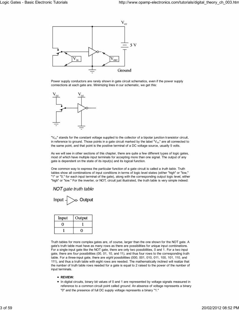
Like an operational amplifier symbol, input and output connections are shown as single wires, theimplied reference point for each voltage signal being "ground." In digital gate circuits, ground isalmost always the negative connection of a single voltage source (power supply). Dual, or "split,"power supplies are seldom used in gate circuitry. Because gate circuits are amplifiers, they requirea source of power to operate. Like operational amplifiers, the power supply connections for digitalgates are often omitted from the symbol for simplicity's sake. If we were to show all the necessaryconnections needed for operating this gate, the schematic would look something like this:
Power supply conductors are rarely shown in gate circuit schematics, even if the power supplyconnections at each gate are. Minimizing lines in our schematic, we get this:
"Vcc" stands for the constant voltage supplied to the collector of a bipolar junction transistor circuit,in reference to ground. Those points in a gate circuit marked by the label "Vcc" are all connected tothe same point, and that point is the positive terminal of a DC voltage source, usually 5 volts.
As we will see in other sections of this chapter, there are quite a few different types of logic gates,most of which have multiple input terminals for accepting more than one signal. The output of anygate is dependent on the state of its input(s) and its logical function.
One common way to express the particular function of a gate circuit is called a truth table. Truthtables show all combinations of input conditions in terms of logic level states (either "high" or "low,""1" or "0," for each input terminal of the gate), along with the corresponding output logic level, either"high" or "low." For the inverter, or NOT, circuit just illustrated, the truth table is very simple indeed:
Truth tables for more complex gates are, of course, larger than the one shown for the NOT gate. Agate's truth table must have as many rows as there are possibilities for unique input combinations.For a single-input gate like the NOT gate, there are only two possibilities, 0 and 1. For a two inputgate, there are four possibilities (00, 01, 10, and 11), and thus four rows to the corresponding truthtable. For a three-input gate, there are eight possibilities (000, 001, 010, 011, 100, 101, 110, and111), and thus a truth table with eight rows are needed. The mathematically inclined will realize thatthe number of truth table rows needed for a gate is equal to 2 raised to the power of the number ofinput terminals.
REVIEW:In digital circuits, binary bit values of 0 and 1 are represented by voltage signals measured inreference to a common circuit point called ground. An absence of voltage represents a binary"0" and the presence of full DC supply voltage represents a binary "1."
A logic gate, or simply gate, is a special form of amplifier circuit designed to input and outputlogic level voltages (voltages intended to represent binary bits). Gate circuits are mostcommonly represented in a schematic by their own unique symbols rather than by theirconstituent transistors and resistors.Just as with operational amplifiers, the power supply connections to gates are often omittedin schematic diagrams for the sake of simplicity.A truth table is a standard way of representing the input/output relationships of a gate circuit,listing all the possible input logic level combinations with their respective output logic levels.
The NOT gateThe single-transistor inverter circuit illustrated earlier is actually too crude to be of practical use as agate. Real inverter circuits contain more than one transistor to maximize voltage gain (so as toensure that the final output transistor is either in full cutoff or full saturation), and other componentsdesigned to reduce the chance of accidental damage.
Shown here is a schematic diagram for a real inverter circuit, complete with all necessarycomponents for efficient and reliable operation:
This circuit is composed exclusively of resistors and bipolar transistors. Bear in mind that othercircuit designs are capable of performing the NOT gate function, including designs substituting field-effect transistors for bipolar (discussed later in this chapter).
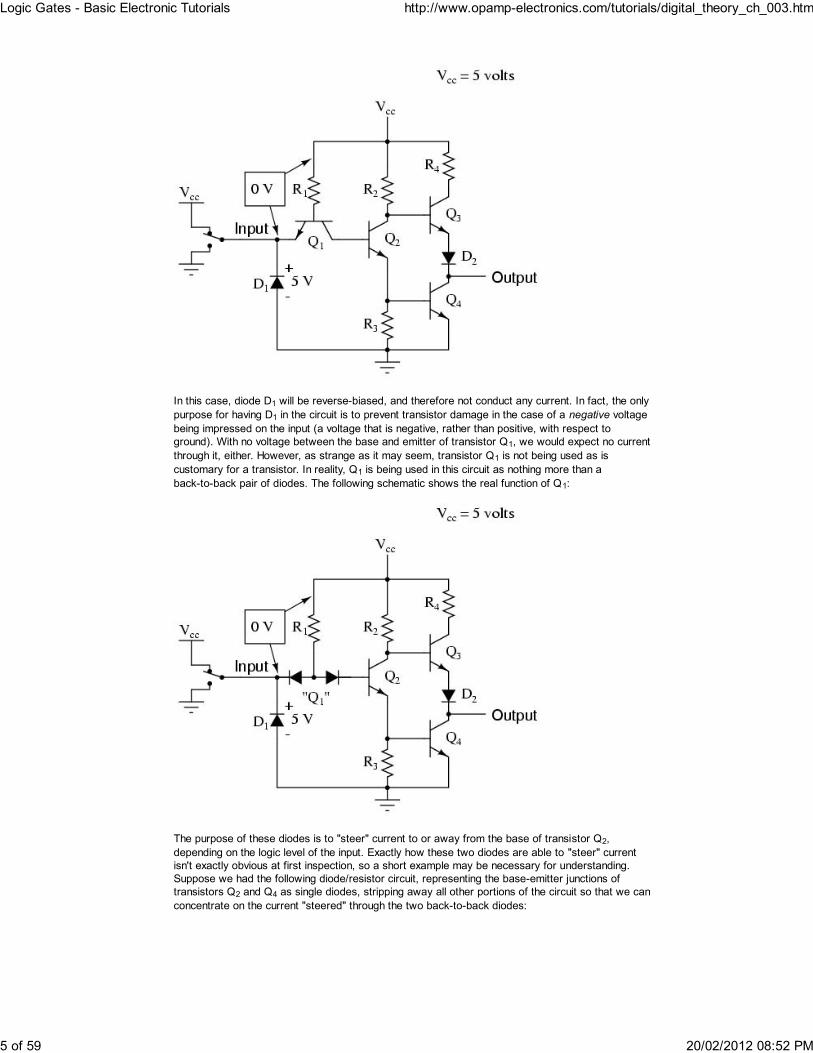
Let's analyze this circuit for the condition where the input is "high," or in a binary "1" state. We cansimulate this by showing the input terminal connected to Vcc through a switch:
In this case, diode D1 will be reverse-biased, and therefore not conduct any current. In fact, the onlypurpose for having D1 in the circuit is to prevent transistor damage in the case of a negative voltagebeing impressed on the input (a voltage that is negative, rather than positive, with respect toground). With no voltage between the base and emitter of transistor Q1, we would expect no currentthrough it, either. However, as strange as it may seem, transistor Q1 is not being used as iscustomary for a transistor. In reality, Q1 is being used in this circuit as nothing more than aback-to-back pair of diodes. The following schematic shows the real function of Q1:
The purpose of these diodes is to "steer" current to or away from the base of transistor Q2,depending on the logic level of the input. Exactly how these two diodes are able to "steer" currentisn't exactly obvious at first inspection, so a short example may be necessary for understanding.Suppose we had the following diode/resistor circuit, representing the base-emitter junctions oftransistors Q2 and Q4 as single diodes, stripping away all other portions of the circuit so that we canconcentrate on the current "steered" through the two back-to-back diodes:
With the input switch in the "up" position (connected to Vcc), it should be obvious that there will be nocurrent through the left steering diode of Q1, because there isn't any voltage in the switch-diode-R1-switch loop to motivate electrons to flow. However, there will be current through the rightsteering diode of Q1, as well as through Q2's base-emitter diode junction and Q4's base-emitterdiode junction:
This tells us that in the real gate circuit, transistors Q2 and Q4 will have base current, which will turnthem on to conduct collector current. The total voltage dropped between the base of Q1 (the nodejoining the two back-to-back steering diodes) and ground will be about 2.1 volts, equal to thecombined voltage drops of three PN junctions: the right steering diode, Q2's base-emitter diode, andQ4's base-emitter diode.
Now, let's move the input switch to the "down" position and see what happens:
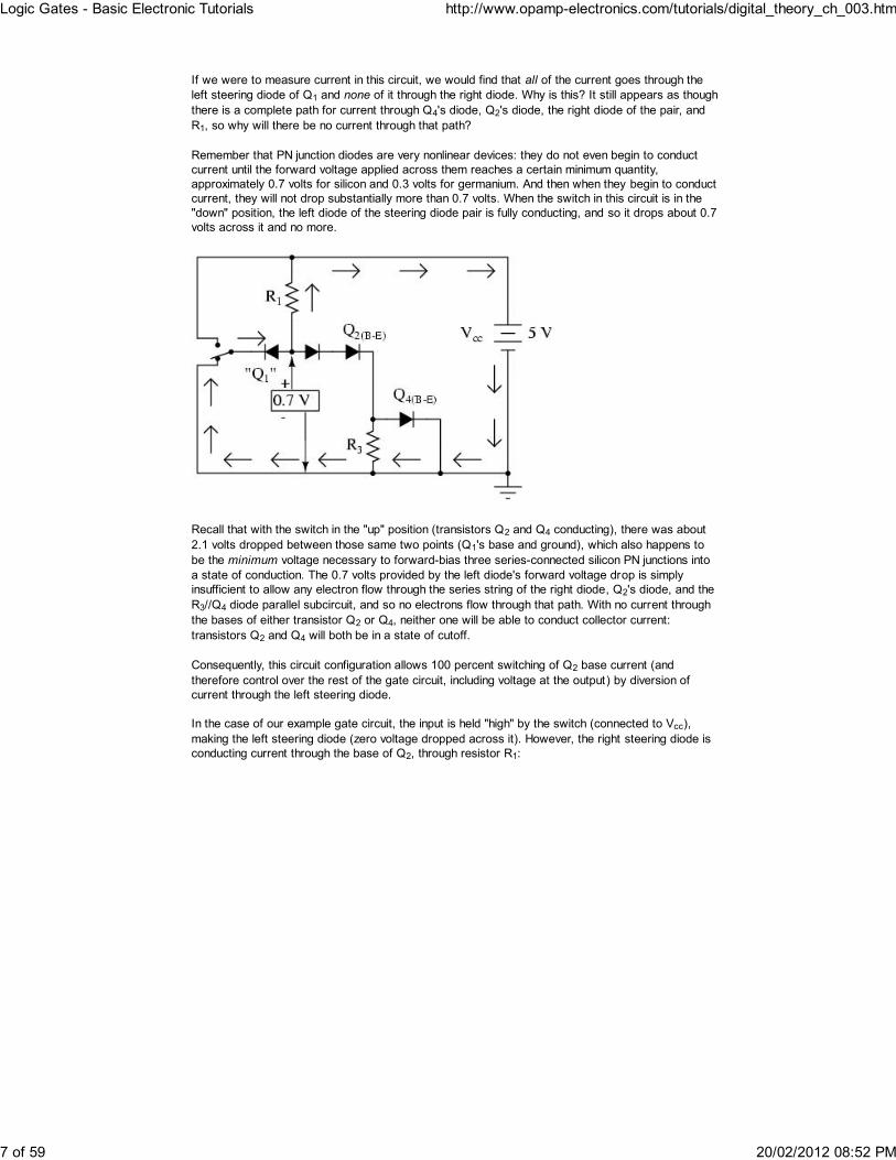
If we were to measure current in this circuit, we would find that all of the current goes through theleft steering diode of Q1 and none of it through the right diode. Why is this? It still appears as thoughthere is a complete path for current through Q4's diode, Q2's diode, the right diode of the pair, andR1, so why will there be no current through that path?
Remember that PN junction diodes are very nonlinear devices: they do not even begin to conductcurrent until the forward voltage applied across them reaches a certain minimum quantity,approximately 0.7 volts for silicon and 0.3 volts for germanium. And then when they begin to conductcurrent, they will not drop substantially more than 0.7 volts. When the switch in this circuit is in the"down" position, the left diode of the steering diode pair is fully conducting, and so it drops about 0.7volts across it and no more.
Recall that with the switch in the "up" position (transistors Q2 and Q4 conducting), there was about2.1 volts dropped between those same two points (Q1's base and ground), which also happens tobe the minimum voltage necessary to forward-bias three series-connected silicon PN junctions intoa state of conduction. The 0.7 volts provided by the left diode's forward voltage drop is simplyinsufficient to allow any electron flow through the series string of the right diode, Q2's diode, and theR3//Q4 diode parallel subcircuit, and so no electrons flow through that path. With no current throughthe bases of either transistor Q2 or Q4, neither one will be able to conduct collector current:transistors Q2 and Q4 will both be in a state of cutoff.
Consequently, this circuit configuration allows 100 percent switching of Q2 base current (andtherefore control over the rest of the gate circuit, including voltage at the output) by diversion ofcurrent through the left steering diode.
In the case of our example gate circuit, the input is held "high" by the switch (connected to Vcc),making the left steering diode (zero voltage dropped across it). However, the right steering diode isconducting current through the base of Q2, through resistor R1:
With base current provided, transistor Q2 will be turned "on." More specifically, it will be saturatedby virtue of the more-than-adequate current allowed by R1 through the base. With Q2 saturated,resistor R3 will be dropping enough voltage to forward-bias the base-emitter junction of transistorQ4, thus saturating it as well:
With Q4 saturated, the output terminal will be almost directly shorted to ground, leaving the outputterminal at a voltage (in reference to ground) of almost 0 volts, or a binary "0" ("low") logic level.Due to the presence of diode D2, there will not be enough voltage between the base of Q3 and itsemitter to turn it on, so it remains in cutoff.
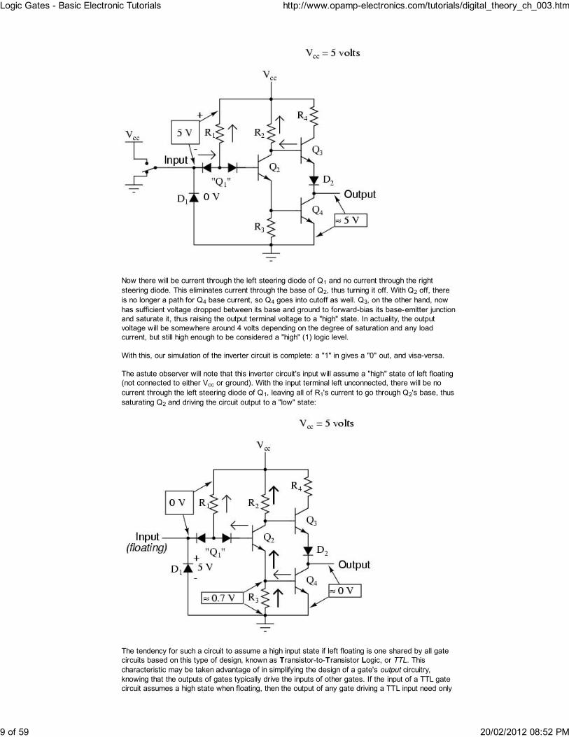
Let's see now what happens if we reverse the input's logic level to a binary "0" by actuating the inputswitch:
Now there will be current through the left steering diode of Q1 and no current through the rightsteering diode. This eliminates current through the base of Q2, thus turning it off. With Q2 off, thereis no longer a path for Q4 base current, so Q4 goes into cutoff as well. Q3, on the other hand, nowhas sufficient voltage dropped between its base and ground to forward-bias its base-emitter junctionand saturate it, thus raising the output terminal voltage to a "high" state. In actuality, the outputvoltage will be somewhere around 4 volts depending on the degree of saturation and any loadcurrent, but still high enough to be considered a "high" (1) logic level.
With this, our simulation of the inverter circuit is complete: a "1" in gives a "0" out, and visa-versa.
The astute observer will note that this inverter circuit's input will assume a "high" state of left floating(not connected to either Vcc or ground). With the input terminal left unconnected, there will be nocurrent through the left steering diode of Q1, leaving all of R1's current to go through Q2's base, thussaturating Q2 and driving the circuit output to a "low" state:
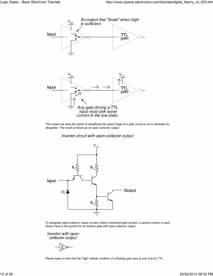
The tendency for such a circuit to assume a high input state if left floating is one shared by all gatecircuits based on this type of design, known as Transistor-to-Transistor Logic, or TTL. Thischaracteristic may be taken advantage of in simplifying the design of a gate's output circuitry,knowing that the outputs of gates typically drive the inputs of other gates. If the input of a TTL gatecircuit assumes a high state when floating, then the output of any gate driving a TTL input need only
provide a path to ground for a low state and be floating for a high state. This concept may requirefurther elaboration for full understanding, so I will explore it in detail here.
A gate circuit as we have just analyzed has the ability to handle output current in two directions: inand out. Technically, this is known as sourcing and sinking current, respectively. When the gateoutput is high, there is continuity from the output terminal to Vcc through the top output transistor(Q3), allowing electrons to flow from ground, through a load, into the gate's output terminal, throughthe emitter of Q3, and eventually up to the Vcc power terminal (positive side of the DC powersupply):
To simplify this concept, we may show the output of a gate circuit as being a double-throw switch,capable of connecting the output terminal either to Vcc or ground, depending on its state. For a gateoutputting a "high" logic level, the combination of Q3 saturated and Q4 cutoff is analogous to adouble-throw switch in the "Vcc" position, providing a path for current through a grounded load:
Please note that this two-position switch shown inside the gate symbol is representative oftransistors Q3 and Q4 alternately connecting the output terminal to Vcc or ground, not of the switchpreviously shown sending an input signal to the gate!
Conversely, when a gate circuit is outputting a "low" logic level to a load, it is analogous to thedouble-throw switch being set in the "ground" position. Current will then be going the other way if theload resistance connects to Vcc: from ground, through the emitter of Q4, out the output terminal,through the load resistance, and back to Vcc. In this condition, the gate is said to be sinking current:
The combination of Q3 and Q4 working as a "push-pull" transistor pair (otherwise known as a totempole output) has the ability to either source current (draw in current to Vcc) or sink current (outputcurrent from ground) to a load. However, a standard TTL gate input never needs current to besourced, only sunk. That is, since a TTL gate input naturally assumes a high state if left floating, anygate output driving a TTL input need only sink current to provide a "0" or "low" input, and need notsource current to provide a "1" or a "high" logic level at the input of the receiving gate:
This means we have the option of simplifying the output stage of a gate circuit so as to eliminate Q3altogether. The result is known as an open-collector output:
To designate open-collector output circuitry within a standard gate symbol, a special marker is used.Shown here is the symbol for an inverter gate with open-collector output:
Please keep in mind that the "high" default condition of a floating gate input is only true for TTL
circuitry, and not necessarily for other types, especially for logic gates constructed of field-effecttransistors.
REVIEW:An inverter, or NOT, gate is one that outputs the opposite state as what is input. That is, a"low" input (0) gives a "high" output (1), and visa-versa.Gate circuits constructed of resistors and bipolar transistors as illustrated in this section arecalled TTL. TTL is an acronym standing for Transistor-to-Transistor Logic. There are otherdesign methodologies used in gate circuits, some which use field-effect transistors ratherthan bipolar transistors.A gate is said to be sourcing current when it provides a path for current between the outputterminal and the positive side of the DC power supply (Vcc). In other words, it is connectingthe output terminal to the power source (+V).A gate is said to be sinking current when it provides a path for current between the outputterminal and ground. In other words, it is grounding (sinking) the output terminal.Gate circuits with totem pole output stages are able to both source and sink current. Gatecircuits with open-collector output stages are only able to sink current, and not sourcecurrent. Open-collector gates are practical when used to drive TTL gate inputs because TTLinputs don't require current sourcing.
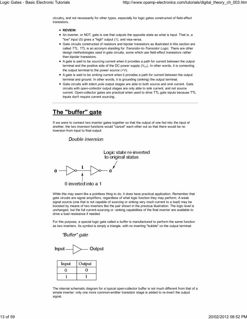
The "buffer" gateIf we were to connect two inverter gates together so that the output of one fed into the input ofanother, the two inversion functions would "cancel" each other out so that there would be noinversion from input to final output:
While this may seem like a pointless thing to do, it does have practical application. Remember thatgate circuits are signal amplifiers, regardless of what logic function they may perform. A weaksignal source (one that is not capable of sourcing or sinking very much current to a load) may beboosted by means of two inverters like the pair shown in the previous illustration. The logic level isunchanged, but the full current-sourcing or -sinking capabilities of the final inverter are available todrive a load resistance if needed.
For this purpose, a special logic gate called a buffer is manufactured to perform the same functionas two inverters. Its symbol is simply a triangle, with no inverting "bubble" on the output terminal:
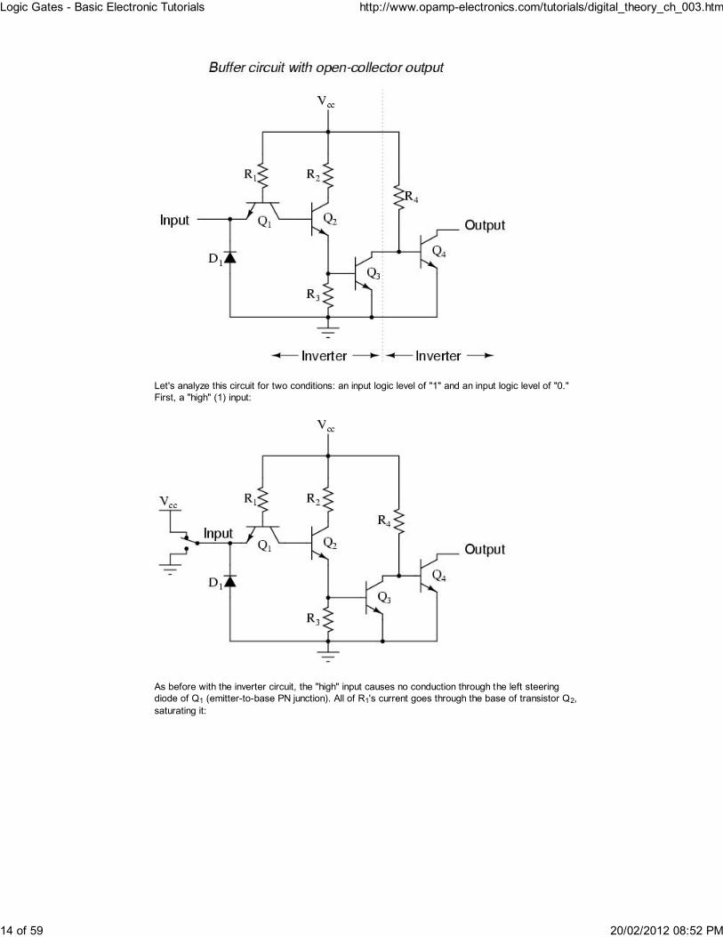
The internal schematic diagram for a typical open-collector buffer is not much different from that of asimple inverter: only one more common-emitter transistor stage is added to re-invert the outputsignal.
Let's analyze this circuit for two conditions: an input logic level of "1" and an input logic level of "0."First, a "high" (1) input:
As before with the inverter circuit, the "high" input causes no conduction through the left steeringdiode of Q1 (emitter-to-base PN junction). All of R1's current goes through the base of transistor Q2,saturating it:
Having Q2 saturated causes Q3 to be saturated as well, resulting in very little voltage droppedbetween the base and emitter of the final output transistor Q4. Thus, Q4 will be in cutoff mode,conducting no current. The output terminal will be floating (neither connected to ground nor Vcc), andthis will be equivalent to a "high" state on the input of the next TTL gate that this one feeds in to.Thus, a "high" input gives a "high" output.
With a "low" input signal (input terminal grounded), the analysis looks something like this:
All of R1's current is now diverted through the input switch, thus eliminating base current through Q2.This forces transistor Q2 into cutoff so that no base current goes through Q3 either. With Q3 cutoffas well, Q4 is will be saturated by the current through resistor R4, thus connecting the outputterminal to ground, making it a "low" logic level. Thus, a "low" input gives a "low" output.
The schematic diagram for a buffer circuit with totem pole output transistors is a bit more complex,but the basic principles, and certainly the truth table, are the same as for the open-collector circuit:
REVIEW:Two inverter, or NOT, gates connected in "series" so as to invert, then re-invert, a binary bitperform the function of a buffer. Buffer gates merely serve the purpose of signalamplification: taking a "weak" signal source that isn't capable of sourcing or sinking muchcurrent, and boosting the current capacity of the signal so as to be able to drive a load.Buffer circuits are symbolized by a triangle symbol with no inverter "bubble."Buffers, like inverters, may be made in open-collector output or totem pole output forms.
Multiple-input gatesInverters and buffers exhaust the possibilities for single-input gate circuits. What more can be donewith a single logic signal but to buffer it or invert it? To explore more logic gate possibilities, we mustadd more input terminals to the circuit(s).
Adding more input terminals to a logic gate increases the number of input state possibilities. With asingle-input gate such as the inverter or buffer, there can only be two possible input states: eitherthe input is "high" (1) or it is "low" (0). As was mentioned previously in this chapter, a two input gatehas four possibilities (00, 01, 10, and 11). A three-input gate has eight possibilities (000, 001, 010,011, 100, 101, 110, and 111) for input states. The number of possible input states is equal to two tothe power of the number of inputs:
This increase in the number of possible input states obviously allows for more complex gatebehavior. Now, instead of merely inverting or amplifying (buffering) a single "high" or "low" logic level,the output of the gate will be determined by whatever combination of 1's and 0's is present at theinput terminals.
Since so many combinations are possible with just a few input terminals, there are many differenttypes of multiple-input gates, unlike single-input gates which can only be inverters or buffers. Eachbasic gate type will be presented in this section, showing its standard symbol, truth table, andpractical operation. The actual TTL circuitry of these different gates will be explored in subsequentsections.
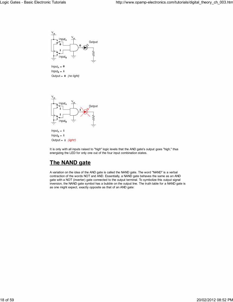
One of the easiest multiple-input gates to understand is the AND gate, so-called because the outputof this gate will be "high" (1) if and only if all inputs (first input and the second input and . . .) are"high" (1). If any input(s) are "low" (0), the output is guaranteed to be in a "low" state as well.
In case you might have been wondering, AND gates are made with more than three inputs, but thisis less common than the simple two-input variety.
A two-input AND gate's truth table looks like this:
What this truth table means in practical terms is shown in the following sequence of illustrations, withthe 2-input AND gate subjected to all possibilities of input logic levels. An LED (Light-Emitting Diode)provides visual indication of the output logic level:
It is only with all inputs raised to "high" logic levels that the AND gate's output goes "high," thusenergizing the LED for only one out of the four input combination states.
The NAND gateA variation on the idea of the AND gate is called the NAND gate. The word "NAND" is a verbalcontraction of the words NOT and AND. Essentially, a NAND gate behaves the same as an ANDgate with a NOT (inverter) gate connected to the output terminal. To symbolize this output signalinversion, the NAND gate symbol has a bubble on the output line. The truth table for a NAND gate isas one might expect, exactly opposite as that of an AND gate:
As with AND gates, NAND gates are made with more than two inputs. In such cases, the samegeneral principle applies: the output will be "low" (0) if and only if all inputs are "high" (1). If any inputis "low" (0), the output will go "high" (1).
The OR gate
Our next gate to investigate is the OR gate, so-called because the output of this gate will be "high"(1) if any of the inputs (first input or the second input or . . .) are "high" (1). The output of an ORgate goes "low" (0) if and only if all inputs are "low" (0).
A two-input OR gate's truth table looks like this:
The following sequence of illustrations demonstrates the OR gate's function, with the 2-inputsexperiencing all possible logic levels. An LED (Light-Emitting Diode) provides visual indication of thegate's output logic level:
A condition of any input being raised to a "high" logic level makes the OR gate's output go "high,"thus energizing the LED for three out of the four input combination states.
As you might have suspected, the NOR gate is an OR gate with its output inverted, just like a NANDgate is an AND gate with an inverted output.
NOR gates, like all the other multiple-input gates seen thus far, can be manufactured with more thantwo inputs. Still, the same logical principle applies: the output goes "low" (0) if any of the inputs aremade "high" (1). The output is "high" (1) only when all inputs are "low" (0).
The Negative-AND gate
A Negative-AND gate functions the same as an AND gate with all its inputs inverted (connectedthrough NOT gates). In keeping with standard gate symbol convention, these inverted inputs aresignified by bubbles. Contrary to most peoples' first instinct, the logical behavior of a Negative-ANDgate is not the same as a NAND gate. Its truth table, actually, is identical to a NOR gate:
Following the same pattern, a Negative-OR gate functions the same as an OR gate with all its inputsinverted. In keeping with standard gate symbol convention, these inverted inputs are signified bybubbles. The behavior and truth table of a Negative-OR gate is the same as for a NAND gate:
The last six gate types are all fairly direct variations on three basic functions: AND, OR, and NOT.The Exclusive-OR gate, however, is something quite different.
Exclusive-OR gates output a "high" (1) logic level if the inputs are at different logic levels, either 0and 1 or 1 and 0. Conversely, they output a "low" (0) logic level if the inputs are at the same logiclevels. The Exclusive-OR (sometimes called XOR) gate has both a symbol and a truth table patternthat is unique:
There are equivalent circuits for an Exclusive-OR gate made up of AND, OR, and NOT gates, justas there were for NAND, NOR, and the negative-input gates. A rather direct approach to simulatingan Exclusive-OR gate is to start with a regular OR gate, then add additional gates to inhibit theoutput from going "high" (1) when both inputs are "high" (1):
In this circuit, the final AND gate acts as a buffer for the output of the OR gate whenever the NANDgate's output is high, which it is for the first three input state combinations (00, 01, and 10).However, when both inputs are "high" (1), the NAND gate outputs a "low" (0) logic level, whichforces the final AND gate to produce a "low" (0) output.
Another equivalent circuit for the Exclusive-OR gate uses a strategy of two AND gates withinverters, set up to generate "high" (1) outputs for input conditions 01 and 10. A f inal OR gate thenallows either of the AND gates' "high" outputs to create a final "high" output:
Exclusive-OR gates are very useful for circuits where two or more binary numbers are to becompared bit-for-bit, and also for error detection (parity check) and code conversion (binary to Greyand visa-versa).
The Exclusive-NOR gate
Finally, our last gate for analysis is the Exclusive-NOR gate, otherwise known as the XNOR gate. Itis equivalent to an Exclusive-OR gate with an inverted output. The truth table for this gate is exactlyopposite as for the Exclusive-OR gate:
As indicated by the truth table, the purpose of an Exclusive-NOR gate is to output a "high" (1) logiclevel whenever both inputs are at the same logic levels (either 00 or 11).
REVIEW:Rule for an AND gate: output is "high" only if first input and second input are both "high."Rule for an OR gate: output is "high" if input A or input B are "high."Rule for a NAND gate: output is not "high" if both the first input and the second input are"high."Rule for a NOR gate: output is not "high" if either the first input or the second input are "high."A Negative-AND gate behaves like a NOR gate.A Negative-OR gate behaves like a NAND gate.Rule for an Exclusive-OR gate: output is "high" if the input logic levels are different.Rule for an Exclusive-NOR gate: output is "high" if the input logic levels are the same.
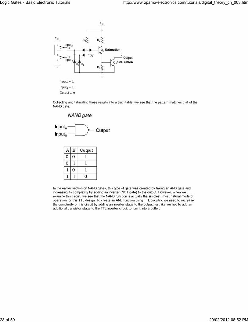
TTL NAND and AND gatesSuppose we altered our basic open-collector inverter circuit, adding a second input terminal just likethe first:
This schematic illustrates a real circuit, but it isn't called a "two-input inverter." Through analysis wewill discover what this circuit's logic function is and correspondingly what it should be designated as.
Just as in the case of the inverter and buffer, the "steering" diode cluster marked "Q1" is actuallyformed like a transistor, even though it isn't used in any amplifying capacity. Unfortunately, a simpleNPN transistor structure is inadequate to simulate the three PN junctions necessary in this diodenetwork, so a different transistor (and symbol) is needed. This transistor has one collector, onebase, and two emitters, and in the circuit it looks like this:
In the single-input (inverter) circuit, grounding the input resulted in an output that assumed the "high"(1) state. In the case of the open-collector output configuration, this "high" state was simply"floating." Allowing the input to float (or be connected to Vcc) resulted in the output becominggrounded, which is the "low" or 0 state. Thus, a 1 in resulted in a 0 out, and visa-versa.
Since this circuit bears so much resemblance to the simple inverter circuit, the only difference beinga second input terminal connected in the same way to the base of transistor Q2, we can say thateach of the inputs will have the same effect on the output. Namely, if either of the inputs aregrounded, transistor Q2 will be forced into a condition of cutoff, thus turning Q3 off and floating theoutput (output goes "high"). The following series of illustrations shows this for three input states (00,01, and 10):
In any case where there is a grounded ("low") input, the output is guaranteed to be floating ("high").Conversely, the only time the output will ever go "low" is if transistor Q3 turns on, which meanstransistor Q2 must be turned on (saturated), which means neither input can be diverting R1 currentaway from the base of Q2. The only condition that will satisfy this requirement is when both inputsare "high" (1):
Collecting and tabulating these results into a truth table, we see that the pattern matches that of theNAND gate:
In the earlier section on NAND gates, this type of gate was created by taking an AND gate andincreasing its complexity by adding an inverter (NOT gate) to the output. However, when weexamine this circuit, we see that the NAND function is actually the simplest, most natural mode ofoperation for this TTL design. To create an AND function using TTL circuitry, we need to increasethe complexity of this circuit by adding an inverter stage to the output, just like we had to add anadditional transistor stage to the TTL inverter circuit to turn it into a buffer:
The truth table and equivalent gate circuit (an inverted-output NAND gate) are shown here:
Of course, both NAND and AND gate circuits may be designed with totem-pole output stages ratherthan open-collector. I am opting to show the open-collector versions for the sake of simplicity.
REVIEW:A TTL NAND gate can be made by taking a TTL inverter circuit and adding another input.An AND gate may be created by adding an inverter stage to the output of the NAND gatecircuit.
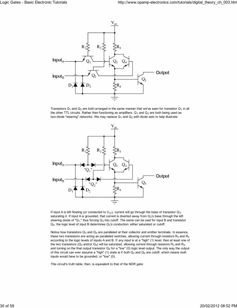
TTL NOR and OR gatesLet's examine the following TTL circuit and analyze its operation:
Transistors Q1 and Q2 are both arranged in the same manner that we've seen for transistor Q1 in allthe other TTL circuits. Rather than functioning as amplifiers, Q1 and Q2 are both being used astwo-diode "steering" networks. We may replace Q1 and Q2 with diode sets to help illustrate:
If input A is left floating (or connected to Vcc), current will go through the base of transistor Q3,saturating it. If input A is grounded, that current is diverted away from Q3's base through the leftsteering diode of "Q1," thus forcing Q3 into cutoff. The same can be said for input B and transistorQ4: the logic level of input B determines Q4's conduction: either saturated or cutoff.
Notice how transistors Q3 and Q4 are paralleled at their collector and emitter terminals. In essence,these two transistors are acting as paralleled switches, allowing current through resistors R3 and R4according to the logic levels of inputs A and B. If any input is at a "high" (1) level, then at least one ofthe two transistors (Q3 and/or Q4) will be saturated, allowing current through resistors R3 and R4,and turning on the final output transistor Q5 for a "low" (0) logic level output. The only way the outputof this circuit can ever assume a "high" (1) state is if both Q3 and Q4 are cutoff, which means bothinputs would have to be grounded, or "low" (0).
This circuit's truth table, then, is equivalent to that of the NOR gate:
In order to turn this NOR gate circuit into an OR gate, we would have to invert the output logic levelwith another transistor stage, just like we did with the NAND-to-AND gate example:
The truth table and equivalent gate circuit (an inverted-output NOR gate) are shown here:
Of course, totem-pole output stages are also possible in both NOR and OR TTL logic circuits.
REVIEW:An OR gate may be created by adding an inverter stage to the output of the NOR gatecircuit.
CMOS gate circuitryUp until this point, our analysis of transistor logic circuits has been limited to the TTL designparadigm, whereby bipolar transistors are used, and the general strategy of floating inputs beingequivalent to "high" (connected to Vcc) inputs -- and correspondingly, the allowance of "open-collector" output stages -- is maintained. This, however, is not the only way we can build logic gates.
Field-effect transistors, particularly the insulated-gate variety, may be used in the design of gatecircuits. Being voltage-controlled rather than current-controlled devices, IGFETs tend to allow verysimple circuit designs. Take for instance, the following inverter circuit built using P- and N-channelIGFETs:
Notice the "Vdd" label on the positive power supply terminal. This label follows the same conventionas "Vcc" in TTL circuits: it stands for the constant voltage applied to the drain of a field effecttransistor, in reference to ground.
Let's connect this gate circuit to a power source and input switch, and examine its operation. Pleasenote that these IGFET transistors are E-type (Enhancement-mode), and so are normally-offdevices. It takes an applied voltage between gate and drain (actually, between gate and substrate)of the correct polarity to bias them on.
The upper transistor is a P-channel IGFET. When the channel (substrate) is made more positivethan the gate (gate negative in reference to the substrate), the channel is enhanced and current isallowed between source and drain. So, in the above illustration, the top transistor is turned on.
The lower transistor, having zero voltage between gate and substrate (source), is in its normalmode: off. Thus, the action of these two transistors are such that the output terminal of the gatecircuit has a solid connection to Vdd and a very high resistance connection to ground. This makes theoutput "high" (1) for the "low" (0) state of the input.
Next, we'll move the input switch to its other position and see what happens:
Now the lower transistor (N-channel) is saturated because it has sufficient voltage of the correctpolarity applied between gate and substrate (channel) to turn it on (positive on gate, negative on thechannel). The upper transistor, having zero voltage applied between its gate and substrate, is in itsnormal mode: off. Thus, the output of this gate circuit is now "low" (0). Clearly, this circuit exhibitsthe behavior of an inverter, or NOT gate.
Using field-effect transistors instead of bipolar transistors has greatly simplified the design of theinverter gate. Note that the output of this gate never floats as is the case with the simplest TTLcircuit: it has a natural "totem-pole" configuration, capable of both sourcing and sinking load current.Key to this gate circuit's elegant design is the complementary use of both P- and N-channel IGFETs.Since IGFETs are more commonly known as MOSFETs (Metal-Oxide-Semiconductor Field EffectTransistor), and this circuit uses both P- and N-channel transistors together, the generalclassification given to gate circuits like this one is CMOS: Complementary Metal OxideSemiconductor.
CMOS circuits aren't plagued by the inherent nonlinearities of the field-effect transistors, because as
digital circuits their transistors always operate in either the saturated or cutoff modes and never inthe active mode. Their inputs are, however, sensitive to high voltages generated by electrostatic(static electricity) sources, and may even be activated into "high" (1) or "low" (0) states by spuriousvoltage sources if left floating. For this reason, it is inadvisable to allow a CMOS logic gate input tofloat under any circumstances. Please note that this is very different from the behavior of a TTL gatewhere a floating input was safely interpreted as a "high" (1) logic level.
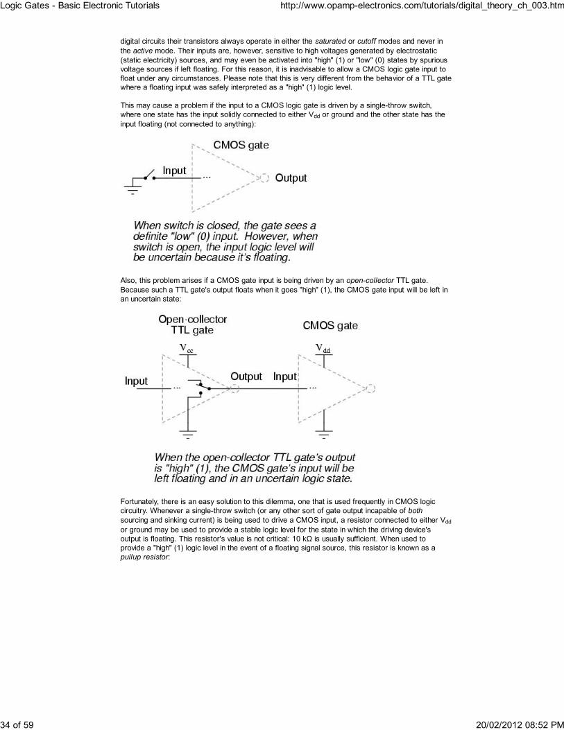
This may cause a problem if the input to a CMOS logic gate is driven by a single-throw switch,where one state has the input solidly connected to either Vdd or ground and the other state has theinput floating (not connected to anything):
Also, this problem arises if a CMOS gate input is being driven by an open-collector TTL gate.Because such a TTL gate's output floats when it goes "high" (1), the CMOS gate input will be left inan uncertain state:
Fortunately, there is an easy solution to this dilemma, one that is used frequently in CMOS logiccircuitry. Whenever a single-throw switch (or any other sort of gate output incapable of bothsourcing and sinking current) is being used to drive a CMOS input, a resistor connected to either Vddor ground may be used to provide a stable logic level for the state in which the driving device'soutput is floating. This resistor's value is not critical: 10 kΩ is usually sufficient. When used toprovide a "high" (1) logic level in the event of a floating signal source, this resistor is known as apullup resistor:
When such a resistor is used to provide a "low" (0) logic level in the event of a floating signal source,it is known as a pulldown resistor. Again, the value for a pulldown resistor is not critical:
Because open-collector TTL outputs always sink, never source, current, pullup resistors arenecessary when interfacing such an output to a CMOS gate input:
Although the CMOS gates used in the preceding examples were all inverters (single-input), the sameprinciple of pullup and pulldown resistors applies to multiple-input CMOS gates. Of course, aseparate pullup or pulldown resistor will be required for each gate input:
This brings us to the next question: how do we design multiple-input CMOS gates such as AND,NAND, OR, and NOR? Not surprisingly, the answer(s) to this question reveal a simplicity of designmuch like that of the CMOS inverter over its TTL equivalent.
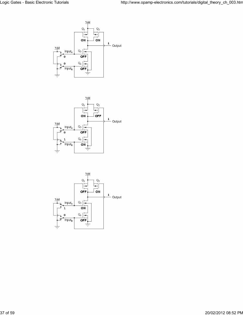
For example, here is the schematic diagram for a CMOS NAND gate:
Notice how transistors Q1 and Q3 resemble the series-connected complementary pair from theinverter circuit. Both are controlled by the same input signal (input A), the upper transistor turning offand the lower transistor turning on when the input is "high" (1), and visa-versa. Notice also howtransistors Q2 and Q4 are similarly controlled by the same input signal (input B), and how they willalso exhibit the same on/off behavior for the same input logic levels. The upper transistors of bothpairs (Q1 and Q2) have their source and drain terminals paralleled, while the lower transistors (Q3and Q4) are series-connected. What this means is that the output will go "high" (1) if either toptransistor saturates, and will go "low" (0) only if both lower transistors saturate. The followingsequence of illustrations shows the behavior of this NAND gate for all four possibilities of input logiclevels (00, 01, 10, and 11):
As with the TTL NAND gate, the CMOS NAND gate circuit may be used as the starting point for thecreation of an AND gate. All that needs to be added is another stage of transistors to invert theoutput signal:
A CMOS NOR gate circuit uses four MOSFETs just like the NAND gate, except that its transistorsare differently arranged. Instead of two paralleled sourcing (upper) transistors connected to Vdd andtwo series-connected sinking (lower) transistors connected to ground, the NOR gate uses twoseries-connected sourcing transistors and two parallel-connected sinking transistors like this:
As with the NAND gate, transistors Q1 and Q3 work as a complementary pair, as do transistors Q2and Q4. Each pair is controlled by a single input signal. If either input A or input B are "high" (1), atleast one of the lower transistors (Q3 or Q4) will be saturated, thus making the output "low" (0). Onlyin the event of both inputs being "low" (0) will both lower transistors be in cutoff mode and bothupper transistors be saturated, the conditions necessary for the output to go "high" (1). Thisbehavior, of course, defines the NOR logic function.
The OR function may be built up from the basic NOR gate with the addition of an inverter stage onthe output:
Since it appears that any gate possible to construct using TTL technology can be duplicated inCMOS, why do these two "families" of logic design still coexist? The answer is that both TTL andCMOS have their own unique advantages.
First and foremost on the list of comparisons between TTL and CMOS is the issue of power
consumption. In this measure of performance, CMOS is the unchallenged victor. Because thecomplementary P- and N-channel MOSFET pairs of a CMOS gate circuit are (ideally) neverconducting at the same time, there is little or no current drawn by the circuit from the Vdd powersupply except for what current is necessary to source current to a load. TTL, on the other hand,cannot function without some current drawn at all times, due to the biasing requirements of thebipolar transistors from which it is made.
There is a caveat to this advantage, though. While the power dissipation of a TTL gate remainsrather constant regardless of its operating state(s), a CMOS gate dissipates more power as thefrequency of its input signal(s) rises. If a CMOS gate is operated in a static (unchanging) condition,it dissipates zero power (ideally). However, CMOS gate circuits draw transient current during everyoutput state switch from "low" to "high" and visa-versa. So, the more often a CMOS gate switchesmodes, the more often it will draw current from the Vdd supply, hence greater power dissipation atgreater frequencies.
A CMOS gate also draws much less current from a driving gate output than a TTL gate becauseMOSFETs are voltage-controlled, not current-controlled, devices. This means that one gate candrive many more CMOS inputs than TTL inputs. The measure of how many gate inputs a single gateoutput can drive is called fanout.
Another advantage that CMOS gate designs enjoy over TTL is a much wider allowable range ofpower supply voltages. Whereas TTL gates are restricted to power supply (Vcc) voltages between4.75 and 5.25 volts, CMOS gates are typically able to operate on any voltage between 3 and 15volts! The reason behind this disparity in power supply voltages is the respective bias requirementsof MOSFET versus bipolar junction transistors. MOSFETs are controlled exclusively by gate voltage(with respect to substrate), whereas BJTs are current-controlled devices. TTL gate circuitresistances are precisely calculated for proper bias currents assuming a 5 volt regulated powersupply. Any significant variations in that power supply voltage will result in the transistor biascurrents being incorrect, which then results in unreliable (unpredictable) operation. The only effectthat variations in power supply voltage have on a CMOS gate is the voltage definition of a "high" (1)state. For a CMOS gate operating at 15 volts of power supply voltage (Vdd), an input signal must beclose to 15 volts in order to be considered "high" (1). The voltage threshold for a "low" (0) signalremains the same: near 0 volts.
One decided disadvantage of CMOS is slow speed, as compared to TTL. The input capacitances ofa CMOS gate are much, much greater than that of a comparable TTL gate -- owing to the use ofMOSFETs rather than BJTs -- and so a CMOS gate will be slower to respond to a signal transition(low-to-high or visa-versa) than a TTL gate, all other factors being equal. The RC time constantformed by circuit resistances and the input capacitance of the gate tend to impede the fast rise- andfall-times of a digital logic level, thereby degrading high-frequency performance.
A strategy for minimizing this inherent disadvantage of CMOS gate circuitry is to "buffer" the outputsignal with additional transistor stages, to increase the overall voltage gain of the device. Thisprovides a faster-transitioning output voltage (high-to-low or low-to-high) for an input voltage slowlychanging from one logic state to another. Consider this example, of an "unbuffered" NOR gateversus a "buffered," or B-series, NOR gate:
In essence, the B-series design enhancement adds two inverters to the output of a simple NORcircuit. This serves no purpose as far as digital logic is concerned, since two cascaded inverterssimply cancel:
However, adding these inverter stages to the circuit does serve the purpose of increasing overallvoltage gain, making the output more sensitive to changes in input state, working to overcome the
inherent slowness caused by CMOS gate input capacitance.
REVIEW:CMOS logic gates are made of IGFET (MOSFET) transistors rather than bipolar junctiontransistors.CMOS gate inputs are sensitive to static electricity. They may be damaged by high voltages,and they may assume any logic level if left floating.Pullup and pulldown resistors are used to prevent a CMOS gate input from floating if beingdriven by a signal source capable only of sourcing or sinking current.CMOS gates dissipate far less power than equivalent TTL gates, but their power dissipationincreases with signal frequency, whereas the power dissipation of a TTL gate isapproximately constant over a wide range of operating conditions.CMOS gate inputs draw far less current than TTL inputs, because MOSFETs are voltage-controlled, not current-controlled, devices.CMOS gates are able to operate on a much wider range of power supply voltages than TTL:typically 3 to 15 volts versus 4.75 to 5.25 volts for TTL.CMOS gates tend to have a much lower maximum operating frequency than TTL gates dueto input capacitances caused by the MOSFET gates.B-series CMOS gates have "buffered" outputs to increase voltage gain from input to output,resulting in faster output response to input signal changes. This helps overcome the inherentslowness of CMOS gates due to MOSFET input capacitance and the RC time constantthereby engendered.
Special-output gatesIt is sometimes desirable to have a logic gate that provides both inverted and non-inverted outputs.For example, a single-input gate that is both a buffer and an inverter, with a separate output terminalfor each function. Or, a two-input gate that provides both the AND and the NAND functions in asingle circuit. Such gates do exist and they are referred to as complementary output gates.
The general symbology for such a gate is the basic gate figure with a bar and two output linesprotruding from it. An array of complementary gate symbols is shown in the following illustration:
Complementary gates are especially useful in "crowded" circuits where there may not be enoughphysical room to mount the additional integrated circuit chips necessary to provide both inverted andnoninverted outputs using standard gates and additional inverters. They are also useful inapplications where a complementary output is necessary from a gate, but the addition of an inverter
would introduce an unwanted time lag in the inverted output relative to the noninverted output. Theinternal circuitry of complemented gates is such that both inverted and noninverted outputs changestate at almost exactly the same time:
Another type of special gate output is called tristate, because it has the ability to provide threedifferent output modes: current sinking ("low" logic level), current sourcing ("high"), and floating("high-Z," or high-impedance). Tristate outputs are usually found as an optional feature on buffergates. Such gates require an extra input terminal to control the "high-Z" mode, and this input isusually called the enable.
With the enable input held "high" (1), the buffer acts like an ordinary buffer with a totem pole outputstage: it is capable of both sourcing and sinking current. However, the output terminal floats (goesinto "high-Z" mode) if ever the enable input is grounded ("low"), regardless of the data signal's logiclevel. In other words, making the enable input terminal "low" (0) effectively disconnects the gatefrom whatever its output is wired to so that it can no longer have any effect.
Tristate buffers are marked in schematic diagrams by a triangle character within the gate symbollike this:
Tristate buffers are also made with inverted enable inputs. Such a gate acts normal when the enableinput is "low" (0) and goes into high-Z output mode when the enable input is "high" (1):
One special type of gate known as the bilateral switch uses gate-controlled MOSFET transistorsacting as on/off switches to switch electrical signals, analog or digital. The "on" resistance of such aswitch is in the range of several hundred ohms, the "off" resistance being in the range of severalhundred mega-ohms.
Bilateral switches appear in schematics as SPST (Single-Pole, Single-Throw) switches inside ofrectangular boxes, with a control terminal on one of the box's long sides:
A bilateral switch might be best envisioned as a solid-state (semiconductor) version of anelectromechanical relay: a signal-actuated switch contact that may be used to conduct virtually anytype of electric signal. Of course, being solid-state, the bilateral switch has none of the undesirable
characteristics of electromechanical relays, such as contact "bouncing," arcing, slow speed, orsusceptibility to mechanical vibration. Conversely, though, they are rather limited in their current-carrying ability. Additionally, the signal conducted by the "contact" must not exceed the power supply"rail" voltages powering the bilateral switch circuit.
Four bilateral switches are packaged inside the popular model "4066" integrated circuit:
REVIEW:Complementary gates provide both inverted and noninverted output signals, in such a waythat neither one is delayed with respect to the other.Tristate gates provide three different output states: high, low, and floating (High-Z). Suchgates are commanded into their high-impedance output modes by a separate input terminalcalled the enable.Bilateral switches are MOSFET circuits providing on/off switching for a variety of electricalsignal types (analog and digital), controlled by logic level voltage signals. In essence, they aresolid-state relays with very low current-handling ability.
Gate universalityNAND and NOR gates possess a special property: they are universal. That is, given enough gates,either type of gate is able to mimic the operation of any other gate type. For example, it is possibleto build a circuit exhibiting the OR function using three interconnected NAND gates. The ability for asingle gate type to be able to mimic any other gate type is one enjoyed only by the NAND and theNOR. In fact, digital control systems have been designed around nothing but either NAND or NORgates, all the necessary logic functions being derived from collections of interconnected NANDs orNORs.
As proof of this property, this section will be divided into subsections showing how all the basic gatetypes may be formed using only NANDs or only NORs.
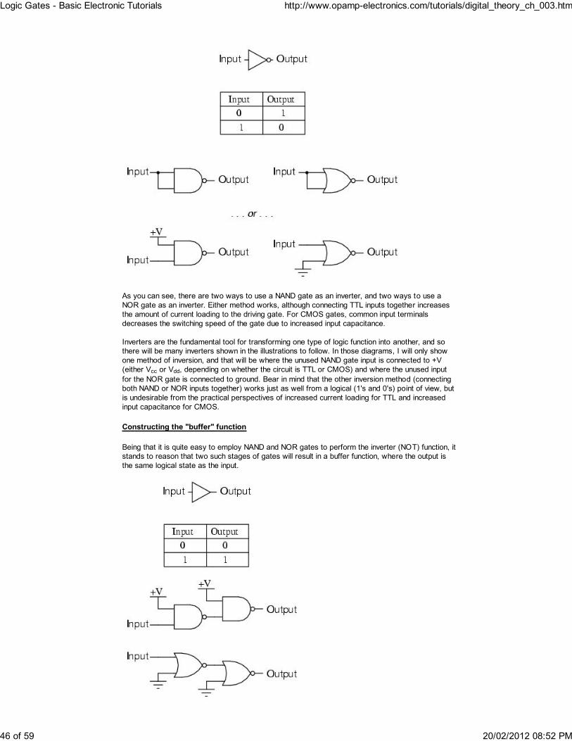
As you can see, there are two ways to use a NAND gate as an inverter, and two ways to use aNOR gate as an inverter. Either method works, although connecting TTL inputs together increasesthe amount of current loading to the driving gate. For CMOS gates, common input terminalsdecreases the switching speed of the gate due to increased input capacitance.
Inverters are the fundamental tool for transforming one type of logic function into another, and sothere will be many inverters shown in the illustrations to follow. In those diagrams, I will only showone method of inversion, and that will be where the unused NAND gate input is connected to +V(either Vcc or Vdd, depending on whether the circuit is TTL or CMOS) and where the unused inputfor the NOR gate is connected to ground. Bear in mind that the other inversion method (connectingboth NAND or NOR inputs together) works just as well from a logical (1's and 0's) point of view, butis undesirable from the practical perspectives of increased current loading for TTL and increasedinput capacitance for CMOS.
Constructing the "buffer" function
Being that it is quite easy to employ NAND and NOR gates to perform the inverter (NOT) function, itstands to reason that two such stages of gates will result in a buffer function, where the output isthe same logical state as the input.
To make the AND function from NAND gates, all that is needed is an inverter (NOT) stage on theoutput of a NAND gate. This extra inversion "cancels out" the first N in NAND, leaving the ANDfunction. It takes a little more work to wrestle the same functionality out of NOR gates, but it can bedone by inverting ("NOT") all of the inputs to a NOR gate.
Constructing the NAND function
It would be pointless to show you how to "construct" the NAND function using a NAND gate, sincethere is nothing to do. To make a NOR gate perform the NAND function, we must invert all inputs tothe NOR gate as well as the NOR gate's output. For a two-input gate, this requires three more NORgates connected as inverters.
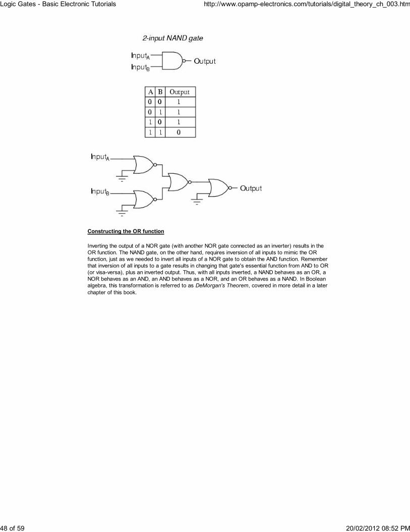
Inverting the output of a NOR gate (with another NOR gate connected as an inverter) results in theOR function. The NAND gate, on the other hand, requires inversion of all inputs to mimic the ORfunction, just as we needed to invert all inputs of a NOR gate to obtain the AND function. Rememberthat inversion of all inputs to a gate results in changing that gate's essential function from AND to OR(or visa-versa), plus an inverted output. Thus, with all inputs inverted, a NAND behaves as an OR, aNOR behaves as an AND, an AND behaves as a NOR, and an OR behaves as a NAND. In Booleanalgebra, this transformation is referred to as DeMorgan's Theorem, covered in more detail in a laterchapter of this book.
REVIEW:NAND and NOR gates are universal: that is, they have the ability to mimic any type of gate, ifinterconnected in sufficient numbers.
Logic signal voltage levelsLogic gate circuits are designed to input and output only two types of signals: "high" (1) and "low"(0), as represented by a variable voltage: full power supply voltage for a "high" state and zerovoltage for a "low" state. In a perfect world, all logic circuit signals would exist at these extremevoltage limits, and never deviate from them (i.e., less than full voltage for a "high," or more than zerovoltage for a "low"). However, in reality, logic signal voltage levels rarely attain these perfect limitsdue to stray voltage drops in the transistor circuitry, and so we must understand the signal levellimitations of gate circuits as they try to interpret signal voltages lying somewhere between fullsupply voltage and zero.
TTL gates operate on a nominal power supply voltage of 5 volts, +/- 0.25 volts. Ideally, a TTL "high"signal would be 5.00 volts exactly, and a TTL "low" signal 0.00 volts exactly. However, real TTL gatecircuits cannot output such perfect voltage levels, and are designed to accept "high" and "low"signals deviating substantially from these ideal values. "Acceptable" input signal voltages range from0 volts to 0.8 volts for a "low" logic state, and 2 volts to 5 volts for a "high" logic state. "Acceptable"output signal voltages (voltage levels guaranteed by the gate manufacturer over a specified range ofload conditions) range from 0 volts to 0.5 volts for a "low" logic state, and 2.7 volts to 5 volts for a"high" logic state:
If a voltage signal ranging between 0.8 volts and 2 volts were to be sent into the input of a TTLgate, there would be no certain response from the gate. Such a signal would be considereduncertain, and no logic gate manufacturer would guarantee how their gate circuit would interpretsuch a signal.
As you can see, the tolerable ranges for output signal levels are narrower than for input signallevels, to ensure that any TTL gate outputting a digital signal into the input of another TTL gate willtransmit voltages acceptable to the receiving gate. The difference between the tolerable output andinput ranges is called the noise margin of the gate. For TTL gates, the low-level noise margin is thedifference between 0.8 volts and 0.5 volts (0.3 volts), while the high-level noise margin is thedifference between 2.7 volts and 2 volts (0.7 volts). Simply put, the noise margin is the peak amountof spurious or "noise" voltage that may be superimposed on a weak gate output voltage signalbefore the receiving gate might interpret it wrongly:
CMOS gate circuits have input and output signal specifications that are quite different from TTL. Fora CMOS gate operating at a power supply voltage of 5 volts, the acceptable input signal voltagesrange from 0 volts to 1.5 volts for a "low" logic state, and 3.5 volts to 5 volts for a "high" logic state."Acceptable" output signal voltages (voltage levels guaranteed by the gate manufacturer over aspecified range of load conditions) range from 0 volts to 0.05 volts for a "low" logic state, and 4.95volts to 5 volts for a "high" logic state:
It should be obvious from these figures that CMOS gate circuits have far greater noise margins thanTTL: 1.45 volts for CMOS low-level and high-level margins, versus a maximum of 0.7 volts for TTL.In other words, CMOS circuits can tolerate over twice the amount of superimposed "noise" voltageon their input lines before signal interpretation errors will result.
CMOS noise margins widen even further with higher operating voltages. Unlike TTL, which isrestricted to a power supply voltage of 5 volts, CMOS may be powered by voltages as high as 15volts (some CMOS circuits as high as 18 volts). Shown here are the acceptable "high" and "low"states, for both input and output, of CMOS integrated circuits operating at 10 volts and 15 volts,respectively:
The margins for acceptable "high" and "low" signals may be greater than what is shown in theprevious illustrations. What is shown represents "worst-case" input signal performance, based onmanufacturer's specifications. In practice, it may be found that a gate circuit will tolerate "high"signals of considerably less voltage and "low" signals of considerably greater voltage than thosespecified here.
Conversely, the extremely small output margins shown -- guaranteeing output states for "high" and"low" signals to within 0.05 volts of the power supply "rails" -- are optimistic. Such "solid" outputvoltage levels will be true only for conditions of minimum loading. If the gate is sourcing or sinkingsubstantial current to a load, the output voltage will not be able to maintain these optimum levels,due to internal channel resistance of the gate's final output MOSFETs.
Within the "uncertain" range for any gate input, there will be some point of demarcation dividing thegate's actual "low" input signal range from its actual "high" input signal range. That is, somewherebetween the lowest "high" signal voltage level and the highest "low" signal voltage level guaranteedby the gate manufacturer, there is a threshold voltage at which the gate will actually switch itsinterpretation of a signal from "low" or "high" or visa-versa. For most gate circuits, this unspecifiedvoltage is a single point:
In the presence of AC "noise" voltage superimposed on the DC input signal, a single threshold pointat which the gate alters its interpretation of logic level will result in an erratic output:
If this scenario looks familiar to you, it's because you remember a similar problem with (analog)voltage comparator op-amp circuits. With a single threshold point at which an input causes theoutput to switch between "high" and "low" states, the presence of significant noise will cause erraticchanges in the output:
The solution to this problem is a bit of positive feedback introduced into the amplifier circuit. With anop-amp, this is done by connecting the output back around to the noninverting (+) input through aresistor. In a gate circuit, this entails redesigning the internal gate circuitry, establishing the feedbackinside the gate package rather than through external connections. A gate so designed is called aSchmitt trigger. Schmitt triggers interpret varying input voltages according to two threshold voltages:a positive-going threshold (VT+), and a negative-going threshold (VT-):
Schmitt trigger gates are distinguished in schematic diagrams by the small "hysteresis" symboldrawn within them, reminiscent of the B-H curve for a ferromagnetic material. Hysteresisengendered by positive feedback within the gate circuitry adds an additional level of noise immunityto the gate's performance. Schmitt trigger gates are frequently used in applications where noise isexpected on the input signal line(s), and/or where an erratic output would be very detrimental tosystem performance.
The differing voltage level requirements of TTL and CMOS technology present problems when thetwo types of gates are used in the same system. Although operating CMOS gates on the same 5.00volt power supply voltage required by the TTL gates is no problem, TTL output voltage levels will notbe compatible with CMOS input voltage requirements.
Take for instance a TTL NAND gate outputting a signal into the input of a CMOS inverter gate. Bothgates are powered by the same 5.00 volt supply (Vcc). If the TTL gate outputs a "low" signal(guaranteed to be between 0 volts and 0.5 volts), it will be properly interpreted by the CMOS gate'sinput as a "low" (expecting a voltage between 0 volts and 1.5 volts):
However, if the TTL gate outputs a "high" signal (guaranteed to be between 5 volts and 2.7 volts), itmight not be properly interpreted by the CMOS gate's input as a "high" (expecting a voltagebetween 5 volts and 3.5 volts):
Given this mismatch, it is entirely possible for the TTL gate to output a valid "high" signal (valid, thatis, according to the standards for TTL) that lies within the "uncertain" range for the CMOS input, andmay be (falsely) interpreted as a "low" by the receiving gate. An easy "fix" for this problem is toaugment the TTL gate's "high" signal voltage level by means of a pullup resistor:
Something more than this, though, is required to interface a TTL output with a CMOS input, if thereceiving CMOS gate is powered by a greater power supply voltage:
There will be no problem with the CMOS gate interpreting the TTL gate's "low" output, of course,but a "high" signal from the TTL gate is another matter entirely. The guaranteed output voltage rangeof 2.7 volts to 5 volts from the TTL gate output is nowhere near the CMOS gate's acceptable rangeof 7 volts to 10 volts for a "high" signal. If we use an open-collector TTL gate instead of atotem-pole output gate, though, a pullup resistor to the 10 volt Vdd supply rail will raise the TTLgate's "high" output voltage to the full power supply voltage supplying the CMOS gate. Since anopen-collector gate can only sink current, not source current, the "high" state voltage level is entirelydetermined by the power supply to which the pullup resistor is attached, thus neatly solving themismatch problem:
Due to the excellent output voltage characteristics of CMOS gates, there is typically no problemconnecting a CMOS output to a TTL input. The only significant issue is the current loading presentedby the TTL inputs, since the CMOS output must sink current for each of the TTL inputs while in the"low" state.
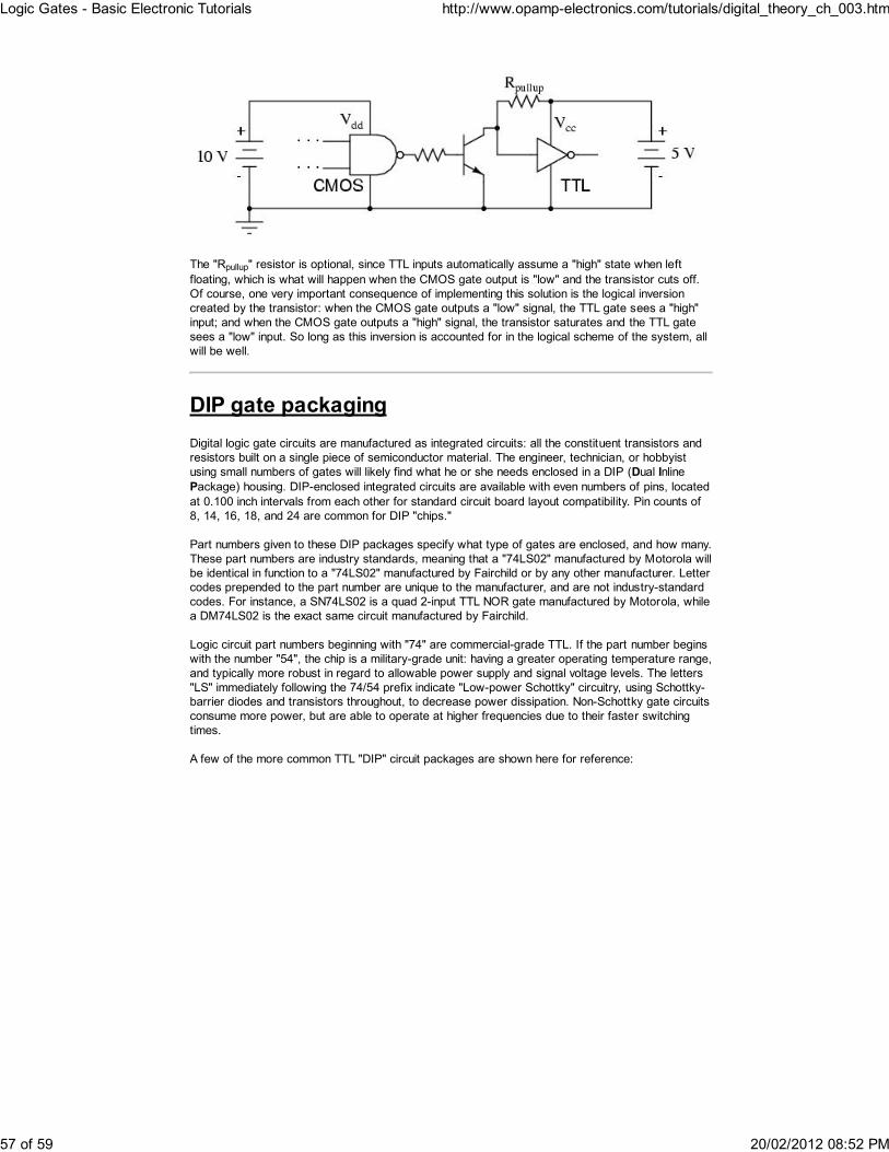
When the CMOS gate in question is powered by a voltage source in excess of 5 volts (Vcc), though,a problem will result. The "high" output state of the CMOS gate, being greater than 5 volts, willexceed the TTL gate's acceptable input limits for a "high" signal. A solution to this problem is tocreate an "open-collector" inverter circuit using a discrete NPN transistor, and use it to interface thetwo gates together:
The "Rpullup" resistor is optional, since TTL inputs automatically assume a "high" state when leftfloating, which is what will happen when the CMOS gate output is "low" and the transistor cuts off.Of course, one very important consequence of implementing this solution is the logical inversioncreated by the transistor: when the CMOS gate outputs a "low" signal, the TTL gate sees a "high"input; and when the CMOS gate outputs a "high" signal, the transistor saturates and the TTL gatesees a "low" input. So long as this inversion is accounted for in the logical scheme of the system, allwill be well.
DIP gate packagingDigital logic gate circuits are manufactured as integrated circuits: all the constituent transistors andresistors built on a single piece of semiconductor material. The engineer, technician, or hobbyistusing small numbers of gates will likely find what he or she needs enclosed in a DIP (Dual InlinePackage) housing. DIP-enclosed integrated circuits are available with even numbers of pins, locatedat 0.100 inch intervals from each other for standard circuit board layout compatibility. Pin counts of8, 14, 16, 18, and 24 are common for DIP "chips."
Part numbers given to these DIP packages specify what type of gates are enclosed, and how many.These part numbers are industry standards, meaning that a "74LS02" manufactured by Motorola willbe identical in function to a "74LS02" manufactured by Fairchild or by any other manufacturer. Lettercodes prepended to the part number are unique to the manufacturer, and are not industry-standardcodes. For instance, a SN74LS02 is a quad 2-input TTL NOR gate manufactured by Motorola, whilea DM74LS02 is the exact same circuit manufactured by Fairchild.
Logic circuit part numbers beginning with "74" are commercial-grade TTL. If the part number beginswith the number "54", the chip is a military-grade unit: having a greater operating temperature range,and typically more robust in regard to allowable power supply and signal voltage levels. The letters"LS" immediately following the 74/54 prefix indicate "Low-power Schottky" circuitry, using Schottky-barrier diodes and transistors throughout, to decrease power dissipation. Non-Schottky gate circuitsconsume more power, but are able to operate at higher frequencies due to their faster switchingtimes.
A few of the more common TTL "DIP" circuit packages are shown here for reference:
Contributors to this chapter are listed in chronological order of their contributions, from most recentto first. See Appendix 2 (Contributor List) for dates and contact information.
Jan-Willem Rensman (May 2, 2002): Suggested the inclusion of Schmitt triggers and gatehysteresis to this chapter.
Lessons In Electric Circuits copyright (C) 2000-2002 Tony R. Kuphaldt, under the terms andconditions of the Design Science License


![Gates and Logic: From Transistors to Logic Gates and Logic ......Gates and Logic: From Transistors to Logic Gates and Logic Circuits [Weatherspoon, Bala, Bracy, and Sirer] Prof. Hakim](https://static.documents.pub/doc/80x56/5fa95cb6eb1af8231472f381/gates-and-logic-from-transistors-to-logic-gates-and-logic-gates-and-logic.jpg)


