45
Chapter 6 Chapter 6 DIFFERENT TYPES OF LOGIC GATES
| Date post: | 25-Mar-2018 |
| Category: |
Documents |
| Upload: | vuongthuan |
| View: | 217 times |
| Download: | 0 times |
Chapter 6Chapter 6
DIFFERENT TYPES OF LOGIC GATES
Ch06L4-"Digital Principles and Design", Raj Kamal, Pearson Education, 2006 2
Lesson 4
TTL Gates
Ch06L4-"Digital Principles and Design", Raj Kamal, Pearson Education, 2006 3
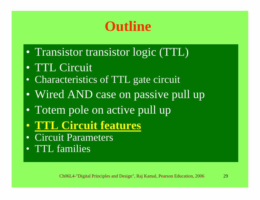
Outline
• Transistor transistor logic (TTL)• TTL Circuit• Characteristics of TTL gate circuit• Wired AND case on passive pull up• Totem pole on active pull up• TTL Circuit features• Circuit Parameters • TTL families
Ch06L4-"Digital Principles and Design", Raj Kamal, Pearson Education, 2006 4
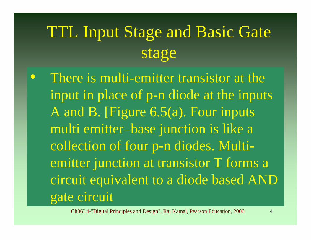
• There is multi-emitter transistor at the input in place of p-n diode at the inputs A and B. [Figure 6.5(a). Four inputs multi emitter–base junction is like a collection of four p-n diodes. Multi-emitter junction at transistor T forms a circuit equivalent to a diode based AND gate circuit
TTL Input Stage and Basic Gate stage
Ch06L4-"Digital Principles and Design", Raj Kamal, Pearson Education, 2006 5
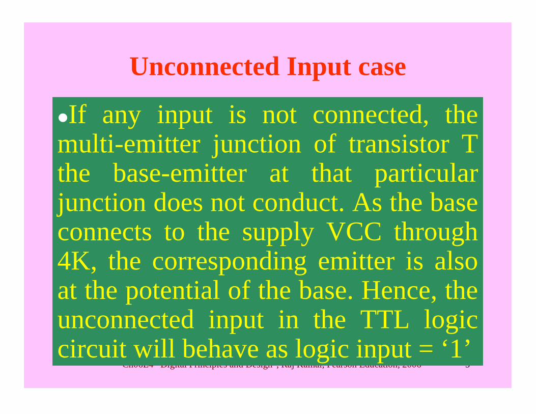
Unconnected Input case
If any input is not connected, the multi-emitter junction of transistor T the base-emitter at that particular junction does not conduct. As the base connects to the supply VCC through 4K, the corresponding emitter is also at the potential of the base. Hence, the unconnected input in the TTL logic circuit will behave as logic input = ‘1’
Ch06L4-"Digital Principles and Design", Raj Kamal, Pearson Education, 2006 6
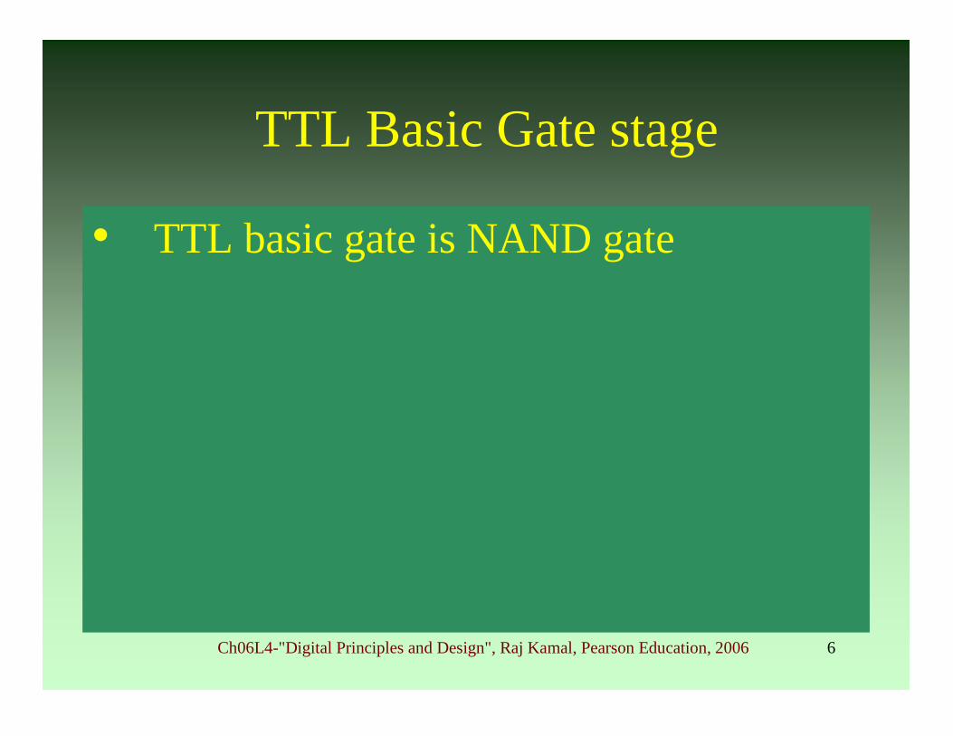
• TTL basic gate is NAND gate
TTL Basic Gate stage
Ch06L4-"Digital Principles and Design", Raj Kamal, Pearson Education, 2006 7
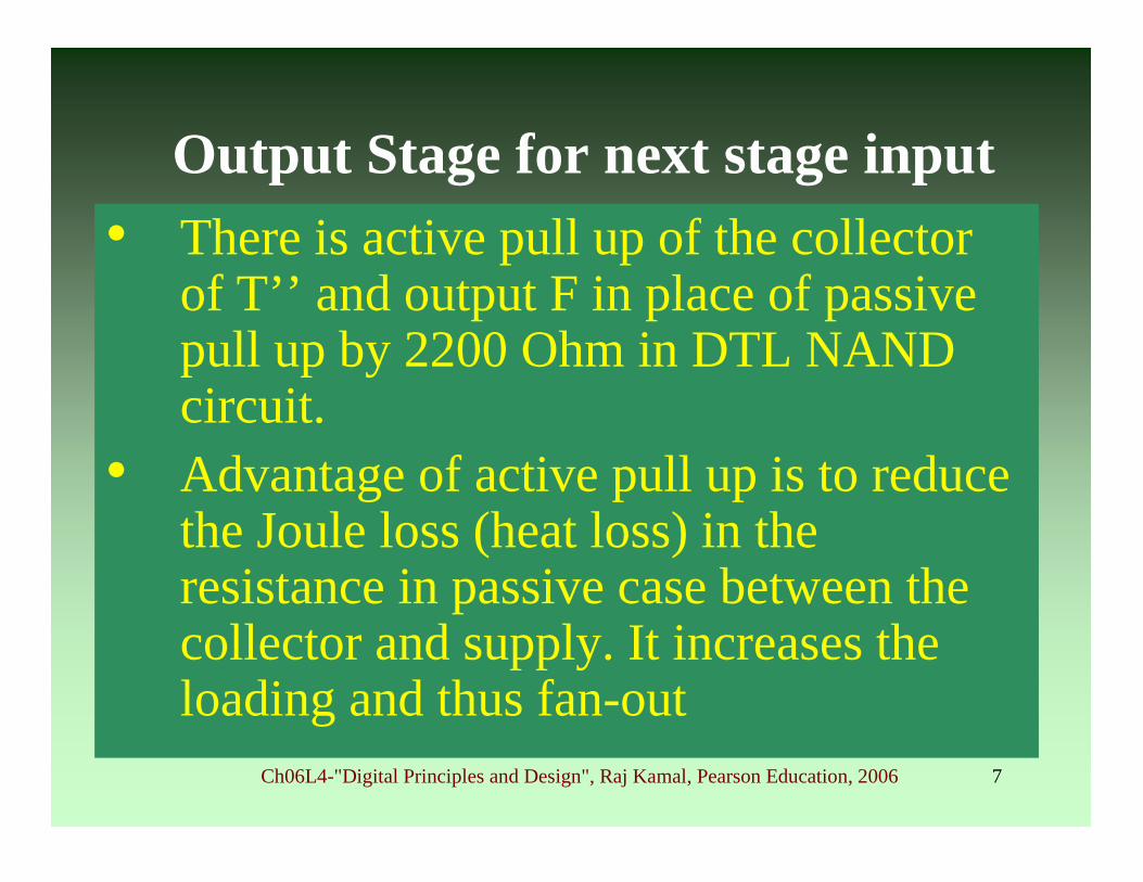
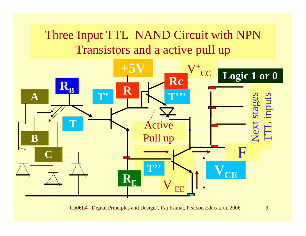
• There is active pull up of the collector of T’’ and output F in place of passive pull up by 2200 Ohm in DTL NAND circuit.
• Advantage of active pull up is to reduce the Joule loss (heat loss) in the resistance in passive case between the collector and supply. It increases the loading and thus fan-out
Output Stage for next stage input
Ch06L4-"Digital Principles and Design", Raj Kamal, Pearson Education, 2006 8
Outline
• Transistor transistor logic (TTL)• TTL Circuit• Characteristics of TTL gate circuit• Wired AND case on passive pull up• Totem pole on active pull up• TTL Circuit features• Circuit Parameters • TTL families
Ch06L4-"Digital Principles and Design", Raj Kamal, Pearson Education, 2006 9
Three Input TTL NAND Circuit with NPNTransistors and a active pull up
RB
V-EE
Active Pull up
+5VR
V+CC
B
VCE
Logic 1 or 0
A
T
Nex
t sta
ges
TTL
inpu
ts
C
T’
F
Rc
RE
T’’
T’’’
Ch06L4-"Digital Principles and Design", Raj Kamal, Pearson Education, 2006 10
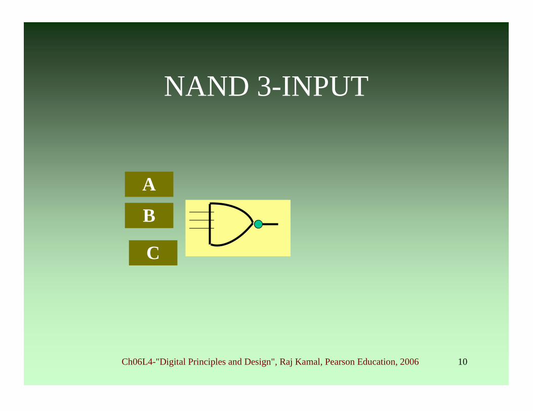
NAND 3-INPUT
BA
C
Ch06L4-"Digital Principles and Design", Raj Kamal, Pearson Education, 2006 11
Output at F A common output from the transistor T’’ at F is given to one (or more) input n-p junction at next TTL stage(s) multi-emitter junction(s).
Ch06L4-"Digital Principles and Design", Raj Kamal, Pearson Education, 2006 12
Outline
• Transistor transistor logic (TTL)• TTL Circuit• Characteristics of TTL gate circuit• Wired AND case on passive pull up• Totem pole on active pull up• TTL Circuit features• Circuit Parameters • TTL families
Ch06L4-"Digital Principles and Design", Raj Kamal, Pearson Education, 2006 13
Noise Margin at 0 For logic state 0, the output at F can be ~0.0 V and maximum 0.8V, else the Tj will start conducting and go in saturation. Hence noise margin of logic state 0 in TTL based logic circuit is 0.8V
Ch06L4-"Digital Principles and Design", Raj Kamal, Pearson Education, 2006 14
Noise Margin at 1 Logic output 1 at F can be between the 2.8 V and 5.0V For logic 1, noise margin will be 3.2VLogic input 1 at F can be between the 2.4 V and 5.0V For logic 1, noise margin will be 3.6V at input.
Ch06L4-"Digital Principles and Design", Raj Kamal, Pearson Education, 2006 15
Next Input Stages driven by output at F
Let C is the capacitance between collector of T’’ (output at F) and emitter of T’’ (supply ground).
Ch06L4-"Digital Principles and Design", Raj Kamal, Pearson Education, 2006 16
Next Input Stages driven by output at F
When T’’ is in cutoff mode (output high), the time constant for discharging when T’’goes to saturation mode (output ~ 0.2V) when all logic inputs becomes ‘1’, the time constant is very small (= T’’ output impedance * C) as the T’’ conducting stage impedance is very low (~ 20 Ω).
Ch06L4-"Digital Principles and Design", Raj Kamal, Pearson Education, 2006 17
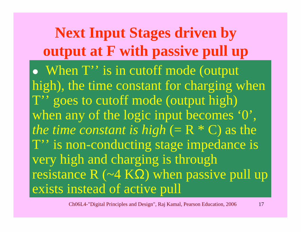
Next Input Stages driven by output at F with passive pull up
When T’’ is in cutoff mode (output high), the time constant for charging when T’’ goes to cutoff mode (output high) when any of the logic input becomes ‘0’, the time constant is high (= R * C) as the T’’ is non-conducting stage impedance is very high and charging is through resistance R (~4 KΩ) when passive pull up exists instead of active pull
Ch06L4-"Digital Principles and Design", Raj Kamal, Pearson Education, 2006 18
Outline
• Transistor transistor logic (TTL)• TTL Circuit• Characteristics of TTL gate circuit• Wired AND case on passive pull up• Totem pole on active pull up• TTL Circuit features• Circuit Parameters • TTL families
Ch06L4-"Digital Principles and Design", Raj Kamal, Pearson Education, 2006 19
TTLCircuit-1
TTL Circuit-2
B
C
A
F
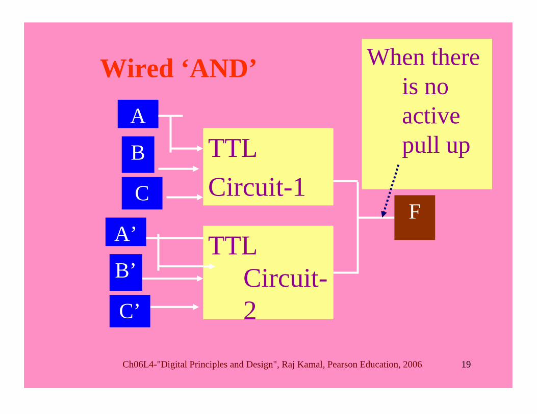
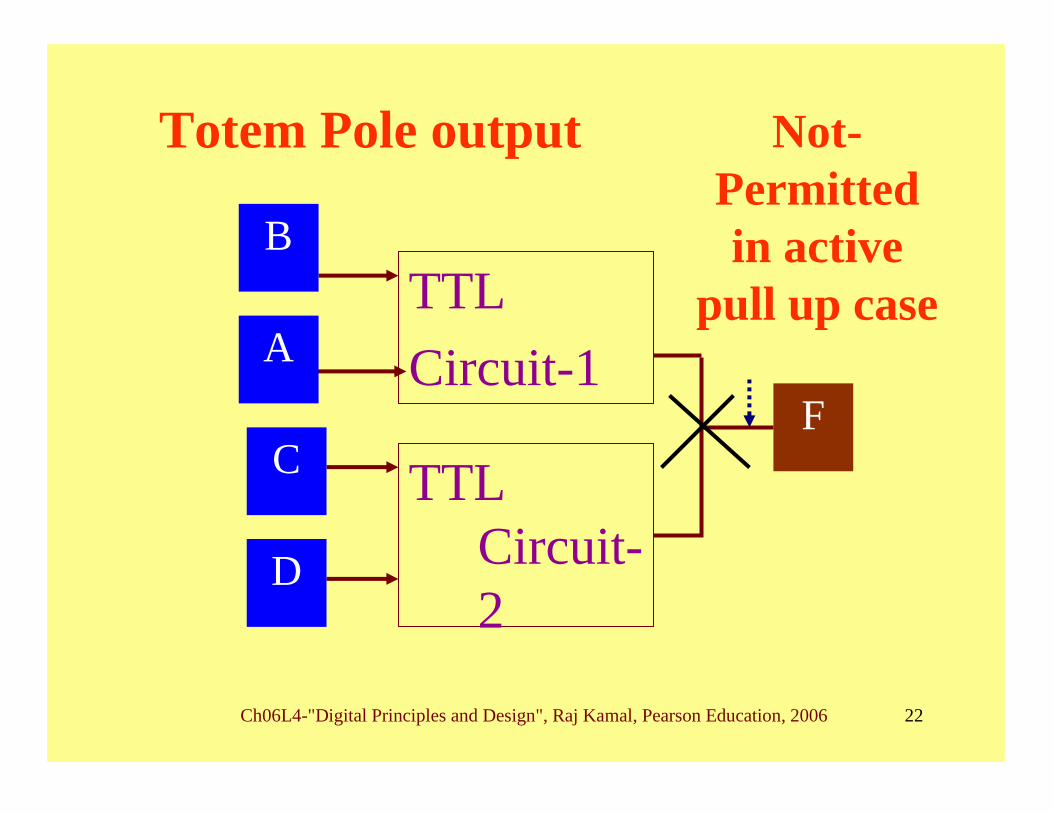
Wired ‘AND’ When there is no active pull up
B’
C’
A’
Ch06L4-"Digital Principles and Design", Raj Kamal, Pearson Education, 2006 20
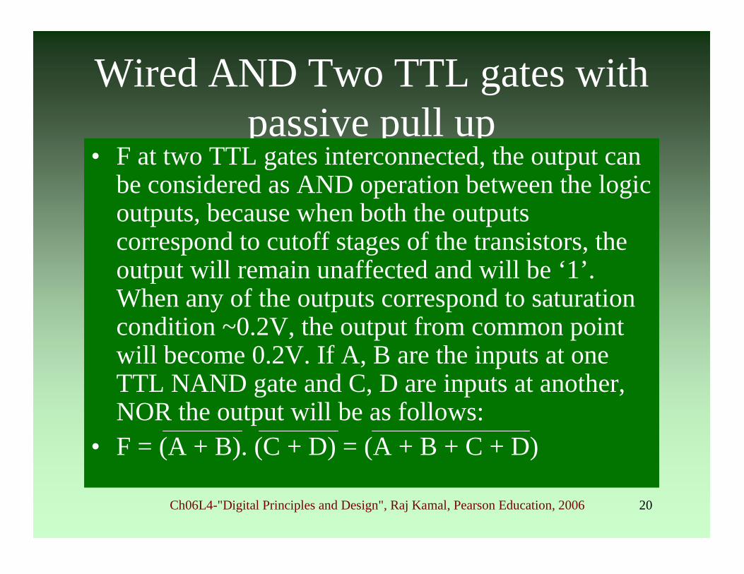
Wired AND Two TTL gates with passive pull up
• F at two TTL gates interconnected, the output can be considered as AND operation between the logic outputs, because when both the outputs correspond to cutoff stages of the transistors, the output will remain unaffected and will be ‘1’. When any of the outputs correspond to saturation condition ~0.2V, the output from common point will become 0.2V. If A, B are the inputs at one TTL NAND gate and C, D are inputs at another, NOR the output will be as follows:
• F = (A + B). (C + D) = (A + B + C + D)
Ch06L4-"Digital Principles and Design", Raj Kamal, Pearson Education, 2006 21
Outline
• Transistor transistor logic (TTL)• TTL Circuit• Characteristics of TTL gate circuit• Wired AND case on passive pull up• Totem pole on active pull up• TTL Circuit features• Circuit Parameters • TTL families
Ch06L4-"Digital Principles and Design", Raj Kamal, Pearson Education, 2006 22
TTLCircuit-1
TTL Circuit-2
B
A
C
D
F
Totem Pole output Not-Permitted in active
pull up case
Ch06L4-"Digital Principles and Design", Raj Kamal, Pearson Education, 2006 23
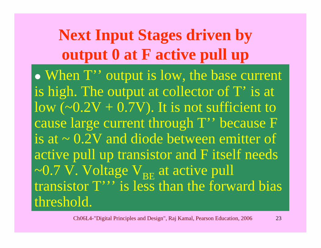
Next Input Stages driven by output 0 at F active pull up
When T’’ output is low, the base current is high. The output at collector of T’ is at low (~0.2V + 0.7V). It is not sufficient to cause large current through T’’ because F is at ~ 0.2V and diode between emitter of active pull up transistor and F itself needs ~0.7 V. Voltage VBE at active pull transistor T’’’ is less than the forward bias threshold.
Ch06L4-"Digital Principles and Design", Raj Kamal, Pearson Education, 2006 24
Next Input Stages driven by output 0at F active pull up
Therefore, the time constant is still controlled by (= T’’ output impedance * C) which is very low. The discharge on high to low transition takes place through T’’ only .
Ch06L4-"Digital Principles and Design", Raj Kamal, Pearson Education, 2006 25
Next Input Stages driven by output 1 at F with active pull up
When T’’ output is high, the base current is very low in cutoff stage. The output at collector of T’ is at high. It is not sufficient to cause large current through T’’ because F is also at high and the diode between emitter of active pull up transistor and F itself needs ~0.7 V.
Ch06L4-"Digital Principles and Design", Raj Kamal, Pearson Education, 2006 26
Next Input Stages driven by output 1 at F with active pull up
Voltage VBE at active pull transistor T’’’is less than the forward bias threshold. The transition of the diode from above threshold to below threshold state will take time.
Ch06L4-"Digital Principles and Design", Raj Kamal, Pearson Education, 2006 27
Next Input Stages driven by output 1 at F with active pull up
However the time constant on charging is still small controlled by (Diode impedance in the beginning conduction state + Base-emitter saturation state resistance in the beginning) * C, which is low.
Ch06L4-"Digital Principles and Design", Raj Kamal, Pearson Education, 2006 28
Next Input Stages driven by output 1 at F with active pull up
These two resistance collectively are ~ 150 Ω (<< 4 kΩ in case of use of passive pull up). This is because the when there is a transition from low to high at output F, the diode and T’’’ will take time to change their conducting state to non-conducting states
Ch06L4-"Digital Principles and Design", Raj Kamal, Pearson Education, 2006 29
Outline
• Transistor transistor logic (TTL)• TTL Circuit• Characteristics of TTL gate circuit• Wired AND case on passive pull up• Totem pole on active pull up• TTL Circuit features• Circuit Parameters • TTL families
Ch06L4-"Digital Principles and Design", Raj Kamal, Pearson Education, 2006 30
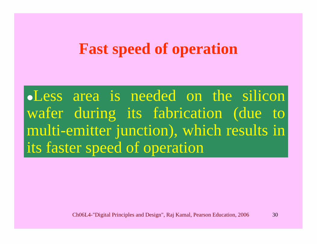
Fast speed of operation
Less area is needed on the silicon wafer during its fabrication (due to multi-emitter junction), which results in its faster speed of operation
Ch06L4-"Digital Principles and Design", Raj Kamal, Pearson Education, 2006 31
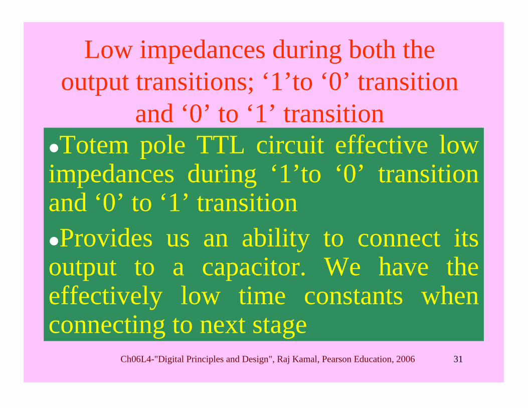
Low impedances during both the output transitions; ‘1’to ‘0’ transition
and ‘0’ to ‘1’ transitionTotem pole TTL circuit effective low impedances during ‘1’to ‘0’ transition and ‘0’ to ‘1’ transitionProvides us an ability to connect its output to a capacitor. We have the effectively low time constants when connecting to next stage
Ch06L4-"Digital Principles and Design", Raj Kamal, Pearson Education, 2006 32
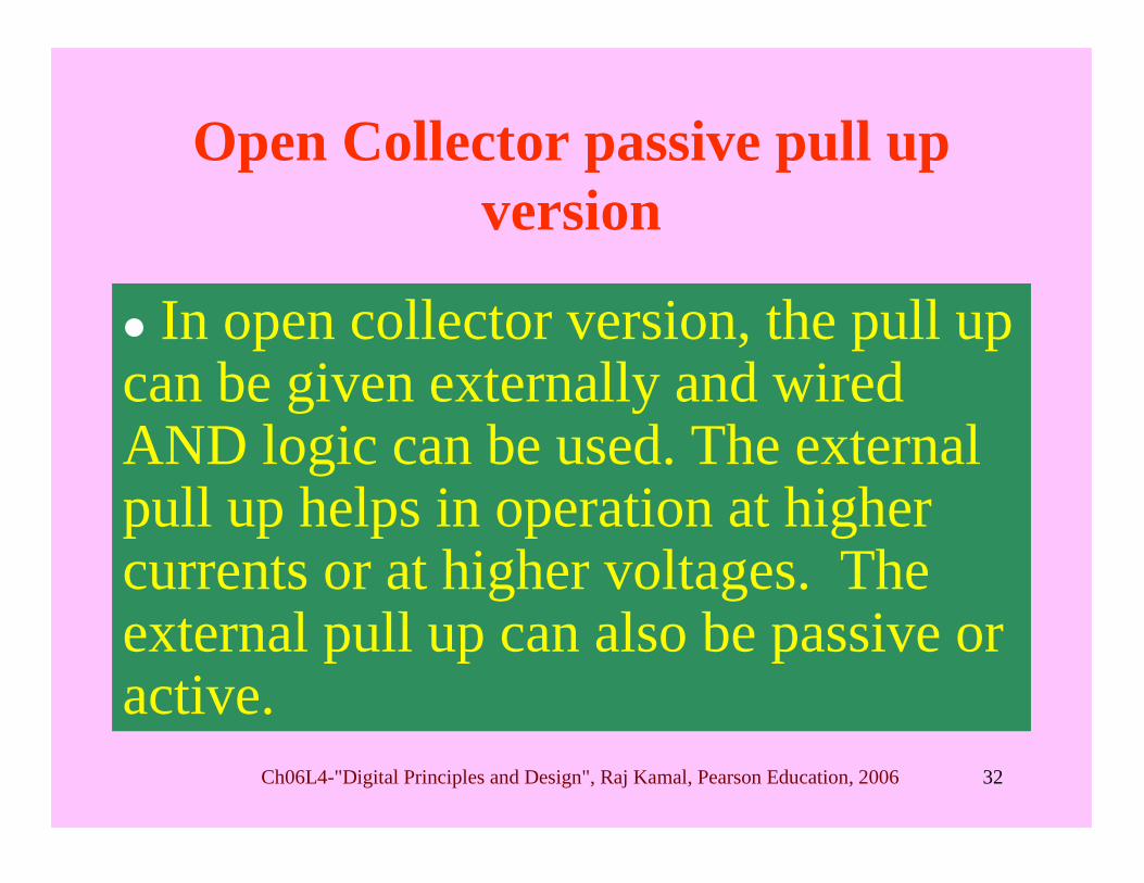
Open Collector passive pull up version
In open collector version, the pull up can be given externally and wired AND logic can be used. The external pull up helps in operation at higher currents or at higher voltages. The external pull up can also be passive or active.
Ch06L4-"Digital Principles and Design", Raj Kamal, Pearson Education, 2006 33
Outline
• Transistor transistor logic (TTL)• TTL Circuit• Characteristics of TTL gate circuit• Wired AND case on passive pull up• Totem pole on active pull up• TTL Circuit features• Circuit Parameters • TTL families
Ch06L4-"Digital Principles and Design", Raj Kamal, Pearson Education, 2006 34
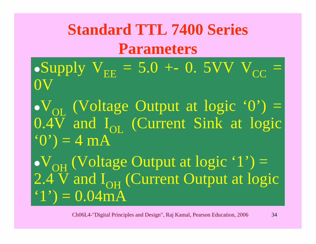
Standard TTL 7400 Series Parameters
Supply VEE = 5.0 +- 0. 5VV VCC = 0VVOL (Voltage Output at logic ‘0’) = 0.4V and IOL (Current Sink at logic ‘0’) = 4 mAVOH (Voltage Output at logic ‘1’) = 2.4 V and IOH (Current Output at logic ‘1’) = 0.04mA
Ch06L4-"Digital Principles and Design", Raj Kamal, Pearson Education, 2006 35
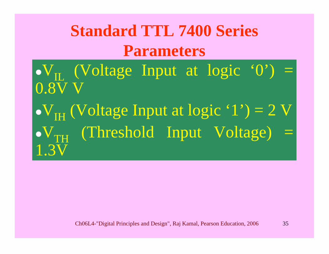
Standard TTL 7400 Series Parameters
VIL (Voltage Input at logic ‘0’) = 0.8V VVIH (Voltage Input at logic ‘1’) = 2 VVTH (Threshold Input Voltage) = 1.3V
Ch06L4-"Digital Principles and Design", Raj Kamal, Pearson Education, 2006 36
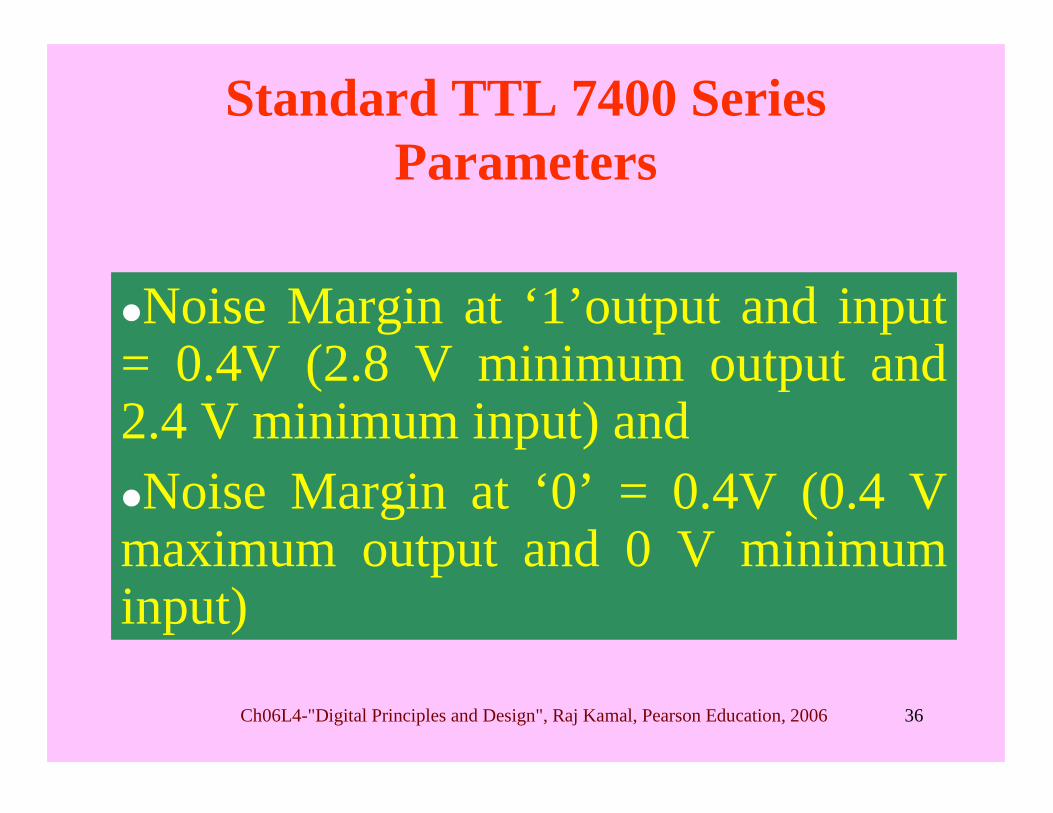
Standard TTL 7400 Series Parameters
Noise Margin at ‘1’output and input = 0.4V (2.8 V minimum output and 2.4 V minimum input) and Noise Margin at ‘0’ = 0.4V (0.4 V maximum output and 0 V minimum input)
Ch06L4-"Digital Principles and Design", Raj Kamal, Pearson Education, 2006 37
Outline
• Transistor transistor logic (TTL)• TTL Circuit• Characteristics of TTL gate circuit• Wired AND case on passive pull up• Totem pole on active pull up• TTL Circuit features• Circuit Parameters • TTL families
Ch06L4-"Digital Principles and Design", Raj Kamal, Pearson Education, 2006 38
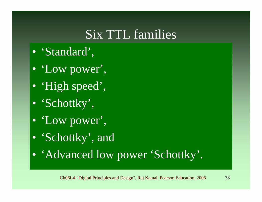
Six TTL families• ‘Standard’, • ‘Low power’, • ‘High speed’, • ‘Schottky’, • ‘Low power’, • ‘Schottky’, and • ‘Advanced low power ‘Schottky’.

Ch06L4-"Digital Principles and Design", Raj Kamal, Pearson Education, 2006 39
Six TTL families• Speed corresponding the 10ns, 33ns,
6ns, 3ns, 10ns and 5ns per gate-propagation-delay times, and
• Power dissipations per gate of 10 mW, 1 mW, 24 mW, 19 mW, 2 mW and 1 mW

Ch06L4-"Digital Principles and Design", Raj Kamal, Pearson Education, 2006 40
Schottky Diodes in 74S, LS, AS• Schottky diode gives high speed of
operation by faster switching of ‘0’ to ‘1’ transitions in a TTL circuit.
• Transistor prevented to become saturated during the transition periods by adding Schottky diode between base and collector
Ch06L4-"Digital Principles and Design", Raj Kamal, Pearson Education, 2006 41
Summary
Ch06L4-"Digital Principles and Design", Raj Kamal, Pearson Education, 2006 42
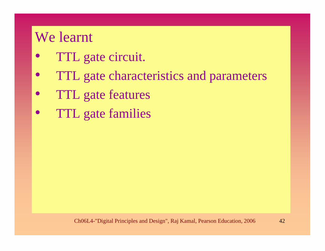
We learnt• TTL gate circuit.• TTL gate characteristics and parameters• TTL gate features• TTL gate families

Ch06L4-"Digital Principles and Design", Raj Kamal, Pearson Education, 2006 43
We learnt• TTL gate has each input connection to a
multi-emitter junction in an n-p-n transistor. It functions as NAND.
• TTL gate has output as totem pole output when there is active pull up and shows same level of time constants in 0 to 1, and 1 to 0 transitions.
• TTL gate has output as Wired OR when there is active pull up and shows different level of time constants in 0 to 1, and 1 to 0 transitions.
Ch06L4-"Digital Principles and Design", Raj Kamal, Pearson Education, 2006 44
End of Lesson 4
TTL Gates

Ch06L4-"Digital Principles and Design", Raj Kamal, Pearson Education, 2006 45
THANK YOU


![Gates and Logic: From Transistors to Logic Gates and Logic ......Gates and Logic: From Transistors to Logic Gates and Logic Circuits [Weatherspoon, Bala, Bracy, and Sirer] Prof. Hakim](https://static.documents.pub/doc/80x56/5fa95cb6eb1af8231472f381/gates-and-logic-from-transistors-to-logic-gates-and-logic-gates-and-logic.jpg)

