IntroductionThe AXI4-Stream FIFO core allows memory mappedaccess to a AXI4-Stream interface. The core can be usedto interface to the AXI Ethernet without the complexityor resource utilization of using DMA.
The principal operation of this core allows the write orread of data packets to or from a device without anyconcern over the AXI4-Stream interface signalling. Themanagement of the AXI4-Stream interfaces istransparent to the user.
Features• 32-bit AXI4-Lite slave interface
• Independent configurable internal TX and RX data FIFOs
• Full duplex operation.
• Supports AXI Ethernet basic mode only
• Provides interrupts for error and status conditions
DS806 July 25, 2012 www.xilinx.com 2Product Specification
LogiCORE IP AXI4-Stream FIFO (v2.01a)
Overview
Figure 1 shows the major components in the AXI4-Stream FIFO core — an AXI Interface block with an AXI4-LiteSlave interface, Interrupt Controller, a Registers module, a Receive Control Module, a Transmit Control Module, aReceive FIFO for the receive data and length, and a Transmit FIFO for the transmit data and the length.
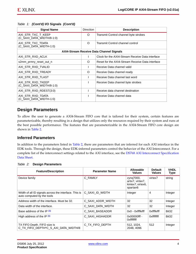
I/O SignalsThe AXI4-Stream FIFO core uses a transparent bus EDK format to simplify the connection of signals between theAXI4-Stream interface of the core and AXI4-Stream interfaces of other IP such as the AXI Ethernet core. Thistechnique allows the EDK tools to automatically connect the AXI signals as an entire group.
When using AXI4-Stream FIFO core with the AXI Ethernet core, connect the three AXI4-Stream interfaces listed:
1. AXI_STR_TXD - AXI4-Stream Transmit Data
2. AXI_STR_TXC - AXI4-Stream Transmit Control
3. AXI_STR_RXD - AXI4-Stream Receive Data
In addition, to support the transmit protocol of the AXI Ethernet core, add the AXI_STR_TxC interface. Thisinterface does not provide any actual data related to the transmit packet data.
The AXI4-Stream FIFO core uses one clock from the AXI4-Lite interface for all clock inputs. When the AXI Ethernetcore is used with the AXI4-Stream FIFO core, all the AXI Stream input clocks of the AXI Ethernet core must use thesame clock.
DS806 July 25, 2012 www.xilinx.com 4Product Specification
LogiCORE IP AXI4-Stream FIFO (v2.01a)
Design ParametersTo allow the user to generate a AXI4-Stream FIFO core that is tailored for their system, certain features areparameterizable, thereby resulting in a design that utilizes only the resources required by their system and runs atthe best possible performance. The features that are parameterizable in the AXI4-Stream FIFO core design areshown in Table 2.
Inferred Parameters
In addition to the parameters listed in Table 2, there are parameters that are inferred for each AXI interface in theEDK tools. Through the design, these EDK-inferred parameters control the behavior of the AXI Interconnect. For acomplete list of the interconnect settings related to the AXI interface, see the DS768 AXI Interconnect SpecificationData Sheet.
AXI_STR_TXC_T_KEEP(C_SAXI_DATA_WIDTH/8-1:0)
O Transmit Control channel byte strobes
AXI_STR_TXC_TDATA(C_SAXI_DATA_WIDTH-1:0)
O Transmit Control channel control
AXI4-Stream Receive Data Channel Signals
AXI_STR_RXD_ACLK I Clock for the AXI4-Stream Receive Data interface
s2mm_prmry_reset_out_n O Reset for the AXI4-Stream Receive Data interface
AXI_STR_RXD_TVALID I Receive Data channel valid
AXI_STR_RXD_TREADY O Receive Data channel ready
AXI_STR_RXD_TLAST I Receive Data channel last word
AXI_STR_RXD_TKEEP(C_SAXI_DATA_WIDTH/8-1:0)
I Receive Data channel byte strobes
AXI_STR_RXD_RDEST(3:0) I Receive data channel destination
AXI_STR_RXD_TDATA(C_SAXI_DATA_WIDTH-1:0)
I Receive Data channel data
Table 2: Design Parameters
Feature/Description Parameter Name Allowable Values
Default Values
VHDL Type
Device family C_FAMILY zynq7000, artix7, virtex7, kintex7, virtex6, spartan6
virtex7 string
Width of all ID signals across the interface. This is auto computed by the tools
C_SAXI_ID_WIDTH Integer 4 Integer
Address width of the interface. Must be 32. C_SAXI_ADDR_WIDTH 32 32 Integer
Data width of the interface. C_SAXI_DATA_WIDTH 32 32 Integer
Base address of the IP (1) C_SAXI_BASEADDR 0x0 - 0xffffefff 0xffffefff Bit32
High address of the IP (1) C_SAXI_HIGHADDR 0x00000fff - 0xffffffff
0xffffffff Bit32
TX FIFO Depth. FIFO size is C_TX_FIFO_DEPTH*C_S_AXI_DATA_WIDTH/8
Notes: 1. HIGHADDR is required to be at least BASEADDR + 4095 because AXI requires a core to have a minimum 4k address space. For
example: C_SAXI_BASEADDR = 0x00000000 and C_SAXI_HIGHADDR = 0x00000FFF. The range specified by BASEADDR and HIGHADDR must be a power of 2 in size, and must have BASEADDR aligned to the size.
X-Ref Target - Figure 2
Figure 2: AXI4-Stream FIFO Connected to an AXI Ethernet Core
Table 2: (Cont’d) Design Parameters (Cont’d)
Feature/Description Parameter Name Allowable Values
DS806 July 25, 2012 www.xilinx.com 6Product Specification
LogiCORE IP AXI4-Stream FIFO (v2.01a)
Figure 3 shows a partial code segment from an EDK MHS file. The file shows an example connection betweenAXI4-Stream FIFO cores and an AXI Ethernet core.X-Ref Target - Figure 3
DS806 July 25, 2012 www.xilinx.com 7Product Specification
LogiCORE IP AXI4-Stream FIFO (v2.01a)
Registers DefinitionThe AXI4-Stream FIFO core contains the registers listed in Table 3.
Interrupt Interface
The interrupt signals generated by the AXI4-Stream FIFO core are managed by the ISR and IER registers. The ISR iscombined with the IER register to define the interrupt interface of the AXI4-Stream FIFO core. An overviewdiagram of the interrupt control structure is show in Figure 4.
Interrupt Status Register (ISR)
The Interrupt Status Register is shown in Figure 5. The Interrupt Status register uses one bit to represent eachinternal interruptible condition.
Table 3: Register Names and Descriptions
Register Name AXI Address Access
Interrupt Status Register (ISR) C_SAXI_BASEADDR + 0x0 Read/Clear on Write (1)
Notes: 1. The latched interruptible condition is cleared by writing a 1 to that bit location. Writing a 1 to a bit location that is 0 has no effect.
Likewise, writing a 0 to a bit location that is 1 has no effect. Multiple bits may be cleared in a single write.2. Reset if written with 0xA5.3. If read, these registers will return 0x0. Writing these registers will have no effect.
DS806 July 25, 2012 www.xilinx.com 8Product Specification
LogiCORE IP AXI4-Stream FIFO (v2.01a)
Once an interruptible condition occurs, it will be captured in this register (represented as the corresponding bitbeing set to 1) even if the condition changes. The latched interruptible condition is cleared by writing a 1 to its bitlocation. Writing a 1 to a bit location that is 0 has no effect. Likewise, writing a 0 to a bit location that is 1 has noeffect. Multiple bits may be cleared in a single write.
For any bit set in the Interrupt Status Register, a corresponding bit must be also set in the Interrupt Enable Registerfor the IP2INTC_Irpt signal to be driven active High out of the AXI4-Stream FIFO core.
The Interrupt Status Register bit definitions are detailed in Table 4.X-Ref Target - Figure 5
Figure 5: Interrupt Status Register (offset 0x0)
Table 4: Interrupt Status Register Bit Definitions
Bit(s) Name Core Access
Reset Value Description
0-18 Reserved Read 0x0 Reserved: These bits are reserved for future definition and will always return all zeros.
19 RFPE Read/Clear on Write of
"1"
0 Receive FIFO Programmable Empty: Generated when the difference of read and write pointers of receive FIFO reaches the programmable EMPTY threshold value.‘0’ = No interrupt pending‘1’ = Interrupt pending
20 RFPF Read/Clear on Write of
"1"
0 Receive FIFO Programmable Full: This interrupt is generated when the difference of read and write pointers of receive FIFO reaches the programmable FULL threshold value.‘0’ = No interrupt pending‘1’ = Interrupt pending
21 TFPE Read/Clear on Write of
"1"
0 Transmit FIFO Programmable Empty: This interrupt is generated when the difference of read and write pointers of transmit FIFO reaches the programmable EMPTY threshold value.‘0’ = No interrupt pending‘1’ = Interrupt pending
22 TFPF Read/Clear on Write of
"1"
0 Transmit FIFO Programmable Full: This interrupt is generated when the difference of read and write pointers of transmit FIFO reaches the programmable FULL threshold value.‘0’ = No interrupt pending‘1’ = Interrupt pending
23 RRC Read/Clear on Write of
"1"
0 Receive Reset Complete: This interrupt indicates that a reset of the receive logic has completed."0" = No interrupt pending."1" = Interrupt pending.
24 TRC Read/Clear on Write of
"1"
0 Transmit Reset Complete: This interrupt indicates that a reset of the transmit logic has completed."0" = No interrupt pending."1" = Interrupt pending.
DS806 July 25, 2012 www.xilinx.com 9Product Specification
LogiCORE IP AXI4-Stream FIFO (v2.01a)
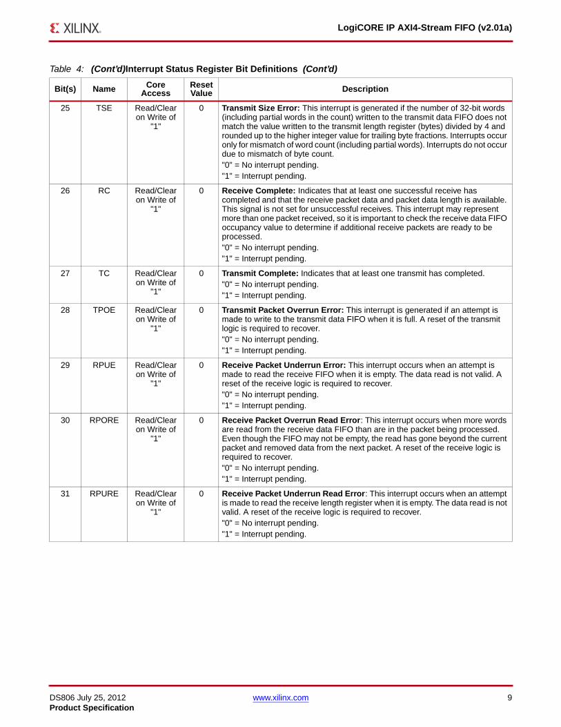
25 TSE Read/Clear on Write of
"1"
0 Transmit Size Error: This interrupt is generated if the number of 32-bit words (including partial words in the count) written to the transmit data FIFO does not match the value written to the transmit length register (bytes) divided by 4 and rounded up to the higher integer value for trailing byte fractions. Interrupts occur only for mismatch of word count (including partial words). Interrupts do not occur due to mismatch of byte count."0" = No interrupt pending."1" = Interrupt pending.
26 RC Read/Clear on Write of
"1"
0 Receive Complete: Indicates that at least one successful receive has completed and that the receive packet data and packet data length is available. This signal is not set for unsuccessful receives. This interrupt may represent more than one packet received, so it is important to check the receive data FIFO occupancy value to determine if additional receive packets are ready to be processed."0" = No interrupt pending."1" = Interrupt pending.
27 TC Read/Clear on Write of
"1"
0 Transmit Complete: Indicates that at least one transmit has completed."0" = No interrupt pending."1" = Interrupt pending.
28 TPOE Read/Clear on Write of
"1"
0 Transmit Packet Overrun Error: This interrupt is generated if an attempt is made to write to the transmit data FIFO when it is full. A reset of the transmit logic is required to recover."0" = No interrupt pending."1" = Interrupt pending.
29 RPUE Read/Clear on Write of
"1"
0 Receive Packet Underrun Error: This interrupt occurs when an attempt is made to read the receive FIFO when it is empty. The data read is not valid. A reset of the receive logic is required to recover."0" = No interrupt pending."1" = Interrupt pending.
30 RPORE Read/Clear on Write of
"1"
0 Receive Packet Overrun Read Error: This interrupt occurs when more words are read from the receive data FIFO than are in the packet being processed. Even though the FIFO may not be empty, the read has gone beyond the current packet and removed data from the next packet. A reset of the receive logic is required to recover."0" = No interrupt pending."1" = Interrupt pending.
31 RPURE Read/Clear on Write of
"1"
0 Receive Packet Underrun Read Error: This interrupt occurs when an attempt is made to read the receive length register when it is empty. The data read is not valid. A reset of the receive logic is required to recover."0" = No interrupt pending."1" = Interrupt pending.
Table 4: (Cont’d)Interrupt Status Register Bit Definitions (Cont’d)
DS806 July 25, 2012 www.xilinx.com 10Product Specification
LogiCORE IP AXI4-Stream FIFO (v2.01a)
Interrupt Enable Register (IER)
The Interrupt Enable Register shown in Figure 6 determines which interrupt sources in the Interrupt Status Registerare allowed to generate interrupts. Setting to "1" in a bit location enables the related interrupt from beingpropagated, while a value of "0" disables it.
Transmit Data FIFO Reset Register (TDFR)
The Transmit Data FIFO Reset Register shown in Figure 7 is not an actual register, but is instead a write-onlyaddress, which when written with a specific value, generates a reset for the Transmit Data FIFO. This reset will notoccur until transmit activity on the TX AXI Stream has completed. The reset can occur only during inactive times onthe TX AXI Stream and will affect only the transmit circuitry in this core, thereby preventing the core on the otherend of the AXI4-Stream from receiving a partial packet which could potentially cause a failure condition in the lattercore.
Because of this mode of operation, it is possible that if the AXI4-Stream becomes unresponsive during anAXI4-Stream transaction, a reset will never occur. For example, this might occur while waiting for the destinationready to go active in the middle of a transfer. In such cases it is necessary to use both the AXI4-Stream Reset and theS_AXI_ARESETN reset.
X-Ref Target - Figure 6
Figure 6: Interrupt Enable Register (offset 0x4)
X-Ref Target - Figure 7
Figure 7: Transmit Data FIFO Reset Register (offset 0x8)
Table 5: Transmit Data FIFO Reset Register Bit Definitions
Bit(s) Name Core Access Reset Value Description
31-0 Reset Key Write N/A Reset Write Value. "0x000000A5" - Generate a reset.Others - No effect.
DS806 July 25, 2012 www.xilinx.com 11Product Specification
LogiCORE IP AXI4-Stream FIFO (v2.01a)
Transmit Data FIFO Vacancy Register (TDFV)
The Transmit Data FIFO Vacancy Register shown in Figure 8 is a read-only register that gives the vacancy status ofthe Transmit Data FIFO.
Transmit Data FIFO Data Write Port (TDFD)
The Transmit Data FIFO Data Write Port shown in Figure 9 is a 32-bit wide address location for writing data into theTransmit Data FIFO. The smallest packet that may be transmitted is four 32-bit words (include partial final word)which corresponds to 13 to 16 bytes. The maximum packet that may be transmitted is limited by the size of the FIFOwhich is 510 (include partial final word) words or 2037 to 2040 bytes.
Receive Data FIFO Reset Register (RDFR)
The Receive Data FIFO Reset Register shown in Figure 10 is not an actual register but, rather a write-only address,which when written with a specific value, generates a reset for the Receive Data FIFO.
This reset will not occur until receive activity on the RX AXI Stream has completed. Only during inactive times onthe RX AXI Stream can a reset occur. It will affect only the receive circuitry in this core. This prevents the core on theother end of the AXI4-Stream from transmitting a partial packet which may cause failure condition in that core.
Because of this mode of operation, it is possible that if the AXI4-Stream interface becomes unresponsive during anAXI4-Stream transaction, that the reset will never occur. An example transaction is if a packet is received over theAXI4-Stream that exceeds the FIFO size of this core causing the core’s destination ready to become inactive in themiddle of a transfer. In this case, an S_AXI_ARESETN reset is needed.
X-Ref Target - Figure 8
Figure 8: Transmit Data FIFO Vacancy Register (offset 0xC)
X-Ref Target - Figure 9
Figure 9: Transmit Data FIFO Data Write Port (offset 0x10)
Table 6: Transmit Data FIFO Data Write Port Bit Definitions
Bit(s) Name Core Access Reset Value Description
31-0 Write Data Value Write N/A Transmit Data FIFO Write Value.
X-Ref Target - Figure 10
Figure 10: Receive Data FIFO Reset Register (offset 0x18)
DS806 July 25, 2012 www.xilinx.com 12Product Specification
LogiCORE IP AXI4-Stream FIFO (v2.01a)
Receive Data FIFO Occupancy Register (RDFO)
The Receive Data FIFO Occupancy Register shown in Figure 11 is a read-only register that gives the occupancystatus of the Receive Data FIFO.
Receive Data FIFO Data Read Port (RDFD)
The Receive Data FIFO Data Read Port shown in Figure 12 is a 32-bit wide address location for reading data fromthe Receive Data FIFO. The smallest packet that may be received is a four 32-bit words packet which corresponds to13 to 16 bytes. The maximum packet that may be received is limited by the size of the FIFO which is 510 words or2037 to 2040 bytes.
Transmit Length Register (TLR)
The Transmit Length Register shown in Figure 13 is used to store packet length values (the number of bytes in thepacket) corresponding to valid packets ready for transmit. The data for the packet is stored in the transmit Data
Table 7: Receive Data FIFO Reset Register Bit Definitions
Bit(s) Name Core Access Reset Value Description
31-0 Reset Key Write N/A Reset Write Value: "0x000000A5" - Generate a reset.Others - No effect.
X-Ref Target - Figure 11
Figure 11: Receive Data FIFO Occupancy Register (offset 0x1C)
Table 8: Receive Data FIFO Occupancy Register Bit Definitions
Bit(s) Name Core Access Reset Value Description
11-0 Occupancy Read 0x0 Receive Data FIFO Occupancy: This is the unsigned value reflecting a current snapshot of the number of 32-bit wide locations in use for data storage in the receive Data FIFO memory core. This value is only updated after a packet is successfully received, and therefore can be used to determine if a receive packet is ready to be processed when a non-0 value is read.
31-12 Reserved Read 0x0 Reserved: These bits are reserved for future definition and will always return all zeros.
X-Ref Target - Figure 12
Figure 12: Receive Data FIFO Data Read Port (offset 0x20)
Table 9: Receive Data FIFO Data Read Port Bit Definitions
Bit(s) Name Core Access Reset Value Description
31-0 Read Data Value Read N/A Receive Data FIFO Read Value.
DS806 July 25, 2012 www.xilinx.com 13Product Specification
LogiCORE IP AXI4-Stream FIFO (v2.01a)
FIFO. The data is written to the AXI4-Stream FIFO core over the AXI4 interface, typically by a processor or DMAcore such the Central DMA (CDMA). When presenting a transmit packet to the AXI4-Stream FIFO core, write thepacket data to the Transmit Data FIFO first, then write the length of the packet into the TLR.
Once the packet length is written to the TLR, it is automatically moved to the Transmit Data FIFO with the packetdata freeing up the TLR for another value. The packet length must be written to the TLR after the packet data iswritten to the transmit data FIFO. It is not valid to write data for multiple packets to the transmit data FIFO beforewriting the packet length values.
The action of writing to the Transmit Length Register is used by the AXI4-Stream FIFO core to initiate theprocessing of transmit packets across the AXI4-Stream interface. This action continues until all of the TLR valuesthat have been stored are processed.
The width of the TLR is wide enough to support packets up to 2048 bytes in length. The smallest packet that maybe transmitted is four 32-bit words (include partial final word) which corresponds to 13 to 16 bytes. The maximumpacket that may be transmitted is limited by the size of the FIFO which is 510 (include partial final word) words or2037 to 2040 bytes.
Receive Length Register (RLR)
The receive length register shown in Figure 14 is used to retrieve packet length values (the number of bytes in thepacket) corresponding to valid packets received. The data for the packet is stored in the Receive Data FIFO.
The length is written by the AXI4-Stream FIFO core when the packet is received across the RX AXI4-Streaminterface and the receive data FIFO has the adequate number of locations to ensure that all of the packet data hasbeen saved.
The RLR should only be read when a receive packet is available for processing (the receive occupancy is not zero).Once the RLR is read, the receive packet data should be read from the receive data FIFO before the RLR is readagain.
The RLR values are stored in the receive data FIFO by the AXI4-Stream FIFO core with the data of each packet. TheRLR value for the subsequent packet to be processed is moved to the RLR when the previous RLR value has beenread.
X-Ref Target - Figure 13
Figure 13: Transmit Length Register (offset 0x14)
Table 10: Transmit Length Register Bit Definitions
Bit(s) Name Core Access Reset Value Description
31-14 Reserved N/A 0x0 Reserved: These bits are reserved for future definition and will always return all zeros.
13-0 TXL Write 0x0 Transmit Length: The number of bytes of the corresponding transmit packet stored in the transmit data FIFO.
DS806 July 25, 2012 www.xilinx.com 14Product Specification
LogiCORE IP AXI4-Stream FIFO (v2.01a)
This register is wide enough to support packets up to 2048 bytes in length. The smallest packet that may be receivedis four 32-bit words (include partial final word) which corresponds to 13 to 16 bytes. The maximum packet that maybe received is limited by the size of the FIFO and is 510 words (include partial final word) or 2037 to 2040 bytes.
AXI4-Stream Reset Register (SRR)
The AXI4-Stream Register shown in Figure 15 is not an actual register. It is a write-only address, which whenwritten with a specific value, generates an immediate reset for the entire core as well as driving a reset on theexternal outputs, s2mm_prmry_reset_out_n, mm2s_prmry_reset_out_n, and mm2s_cntrl_reset_out_n, which canbe used to reset the core on the other end of the AXI4-Stream.
Transmit Destination Register (TDR)
The Transmit Destination Register shown in Figure 16 stores the destination address corresponding to the packet tobe transmitted. When presenting a transmit packet to the AXI4-Stream FIFO core, write the destination address intoTDR first, write the packet data to the Transmit Data FIFO next, and then write the length of the packet into the TLR.
The destination address must be written to the TDR before the packet data is written to the transmit data FIFO.Writing data for multiple packets to the transmit data FIFO before writing the destination address values is not avalid sequence.
X-Ref Target - Figure 14
Figure 14: Receive Length Register (offset 0x24)
Table 11: Receive Length Register Bit Definitions
Bit(s) Name Core Access Reset Value Description
31-14 Reserved Read 0x0 Reserved: These bits are reserved for future definition and will always return all zeros.
13-0 RXL Read 0x0 Receive Length: The number of bytes of the corresponding receive data stored in the receive data FIFO.
DS806 July 25, 2012 www.xilinx.com 15Product Specification
LogiCORE IP AXI4-Stream FIFO (v2.01a)
Receive Destination Register (RDR)
The Receive Destination Register shown in Figure 17 retrieves the destination address corresponding to the validpacket received.
The RDR should only be read when a receive packet is available for processing (the receive occupancy is not zero).Once the RDR is read, the receive packet data should be read from the receive data FIFO before the RDR is readagain. The RDR values are stored in the receive data FIFO by the AXI4-Stream FIFO core with the data of eachpacket. The RDR value for the subsequent packet to be processed is moved to the RDR when the previous RDRvalue has been read.
Reserved Registers
Reading from reserved registers will return zeros and writing to reserved registers will have no effect. However,any accesses to address offset 0x40 and above causes undefined results.
Basic UsageThe AXI4-Stream FIFO core was designed to provide memory-mapped access to an AXI4-Stream interfaceconnected to other IP, such as the AXI Ethernet core. Systems must be built through the Embedded DevelopmentKit (EDK) to attach the AXI4-Stream FIFO core, AXI Ethernet core, processor, memory, interconnect the buses,clocking, and additional embedded components.
DS806 July 25, 2012 www.xilinx.com 16Product Specification
LogiCORE IP AXI4-Stream FIFO (v2.01a)
This section briefly describes the operation of the AXI4-Stream FIFO core through register accesses using the AXIEthernet core as an example.
Packets will automatically be transmitted by writing packet data to the transmit data FIFO followed by writing alength in the TLR.
Receiving packets functions in a manner similar to transmission, except that the steps are reversed. Receiving theISR receive complete interrupt or polling of the receive data FIFO occupancy register (when not zero) indicates thereception of a packet. Reading the RLR provides the packet length in bytes. Given the number of received packetbytes, the appropriate number of reads of the Read data FIFO will provide the packet data.
Table 15 illustrates a power-up read of the registers followed by a transmission and reception of a single packet. Seethe register definitions for further information and options.
Table 15: Sample TX and RX Usage
Register Access Value Activity
Power-up Read of Register Values
ISR Read Word 0x01800000 Read interrupt status register
ISR Write Word 0x0FFFFFFFF Write to clear reset done interrupt bits
ISR Read Word 0x00000000 Read interrupt status register
IER Read Word 0x00000000 Read interrupt enable register
TDFV Read Word 0x000001FE Read the transmit FIFO vacancy
RDFO Read Word 0x00000000 Read the receive FIFO occupancy
TDR Write Word 0x00000002 Transmit Destination address (0x2 = destination device address is 2)
Transmit a Packet
TXFIFO_DATA Write Word 0xFFFFFFFF 4 bytes of data
TXFIFO_DATA Write Word 0x12345678 4 bytes of data
TXFIFO_DATA Write Word 0x00010203 4 bytes of data
TXFIFO_DATA Write Word 0x08090A0B 4 bytes of data
TXFIFO_DATA Write Word 0x10111213 4 bytes of data
TXFIFO_DATA Write Word 0x18191A1B 4 bytes of data
TXFIFO_DATA Write Word 0x20212223 4 bytes of data
TXFIFO_DATA Write Word 0x28292A2B 4 bytes of data
TDFV Read Word 0x000001F6 Read the transmit FIFO vacancy
TLR Write Word 0x00000020 Transmit length (0x20 = 32bytes), this starts transmission
ISR Read Word 0x08000000 A typical value after Tx Complete is indicated by interrupt
ISR Write Word 0x0FFFFFFFF Write to clear reset done interrupt bits
ISR Read Word 0x00000000 Read interrupt status register
TDFV Read Word 0x000001FE Read the transmit FIFO vacancy
Receive a Packet
ISR Read Word 0x04000000 A typical value after Rx Complete is indicated by interrupt
ISR Write Word 0x0FFFFFFFF Write to clear reset done interrupt bits
ISR Read Word 0x00000000 Read interrupt status register
RDFO Read Word 0x00000008 Read the receive FIFO occupancy
DS806 July 25, 2012 www.xilinx.com 17Product Specification
LogiCORE IP AXI4-Stream FIFO (v2.01a)
Design Implementation
Design Tools
The AXI4-Stream FIFO core design is implemented using VHDL code. Xilinx XST is the synthesis tool used forsynthesizing the core.
Target Technology
The target technology is an FPGA listed in the supported device family field of the LogiCORE IP Facts Table.
Device Utilization and Performance Benchmarks
Because the AXI4-Stream FIFO core will be used with other design pieces in the FPGA, the utilization and timingnumbers reported in this section are just estimates. As the AXI4-Stream FIFO core is combined with other pieces ofthe FPGA design, the utilization of FPGA resources and timing of the AXI4-Stream FIFO core design will vary fromthe results reported here. The core benchmarks are shown in Table 16 for a Virtex-6 FPGA and in Table 17 for theSpartan-6 FPGA.
RLR Read Word 0x00000020 Receive length (0x20 =32 bytes) indicates number of bytes to read
RDR Read Word 0x00000002 Receive Destination address (0x2 = destination device address is 2)
RDFO Read Word 0x00000008 Read the receive FIFO occupancy
RXFIFO_DATA Read Word 0xFFFFFFFF 4 bytes of data
RXFIFO_DATA Read Word 0x12345678 4 bytes of data
RXFIFO_DATA Read Word 0x00010203 4 bytes of data
RXFIFO_DATA Read Word 0x08090A0B 4 bytes of data
RXFIFO_DATA Read Word 0x10111213 4 bytes of data
RXFIFO_DATA Read Word 0x18191A1B 4 bytes of data
RXFIFO_DATA Read Word 0x20212223 4 bytes of data
RXFIFO_DATA Read Word 0x28292A2B 4 bytes of packet data and CRC value
RDFO Read Word 0x00000000 Read the receive FIFO occupancy (no further receive packets to process)
Table 16: Performance and Resource Utilization Benchmarks for the Virtex-6 FPGA
Device Resources FMAX (MHz)
Block RAMs Slices Slice Flip- Flops LUTs FMAX
2 452 957 876 150
Table 17: Performance and Resource Utilization Benchmarks for the Spartan-6 FPGA
DS806 July 25, 2012 www.xilinx.com 18Product Specification
LogiCORE IP AXI4-Stream FIFO (v2.01a)
System Performance
To measure the system performance (FMAX) of the AXI4-Stream FIFO core, it was added as the Device Under Test(DUT) to a Virtex-6 FPGA system as shown in Figure 18.
Because the core is used with other design modules in the FPGA, the utilization and timing numbers reported inthis section are estimates only. When this core is combined with other designs in the system, the utilization of FPGAresources and timing of the design will vary from the results reported here.
DS806 July 25, 2012 www.xilinx.com 19Product Specification
LogiCORE IP AXI4-Stream FIFO (v2.01a)
The target FPGA was then filled with logic to drive the LUT and BRAM utilization to approximately 70% and theI/O utilization to approximately 80%. Using the default tool options and the slowest speed grade for the targetFPGA, the resulting target FMAX numbers are shown in Table 18.
The target FMAX is influenced by the exact system and is provided for guidance. It is not a guaranteed value acrossall systems.
X-Ref Target - Figure 18
Figure 18: Virtex-6 and Spartan-6 FPGA System with the AXI4-Stream FIFO core as the DUT
DS806 July 25, 2012 www.xilinx.com 20Product Specification
LogiCORE IP AXI4-Stream FIFO (v2.01a)
Reference Documents1. DS562, AXI Slave Burst
2. DS160, Spartan-6 Family Overview
3. DS150, Virtex-6 Family Overview
4. AXI4 AMBA Protocol Version 2.0 Specification
5. DS180, 7 Series FPGAs Overview
SupportXilinx provides technical support for this LogiCORE product when used as described in the productdocumentation. Xilinx cannot guarantee timing, functionality, or support of product if implemented in devices thatare not defined in the documentation, if customized beyond that allowed in the product documentation, or ifchanges are made to any section of the design labeled DO NOT MODIFY.
Ordering InformationThis Xilinx LogiCORE IP module is provided at no additional cost with the Xilinx Vivado Design Suite and ISEDesign Suite Embedded Edition software under the terms of the Xilinx End User License.
Information about this and other Xilinx LogiCORE IP modules is available at the Xilinx Intellectual Property page.For information on pricing and availability of other Xilinx LogiCORE modules and software, please contact yourlocal Xilinx sales representative.
Revision History and
Notice of DisclaimerXilinx is providing this product documentation, hereinafter “Information,” to you “AS IS” with no warranty of any kind, expressor implied. Xilinx makes no representation that the Information, or any particular implementation thereof, is free from anyclaims of infringement. You are responsible for obtaining any rights you may require for any implementation based on theInformation. All specifications are subject to change without notice. XILINX EXPRESSLY DISCLAIMS ANY WARRANTYWHATSOEVER WITH RESPECT TO THE ADEQUACY OF THE INFORMATION OR ANY IMPLEMENTATION BASEDTHEREON, INCLUDING BUT NOT LIMITED TO ANY WARRANTIES OR REPRESENTATIONS THAT THISIMPLEMENTATION IS FREE FROM CLAIMS OF INFRINGEMENT AND ANY IMPLIED WARRANTIES OFMERCHANTABILITY OR FITNESS FOR A PARTICULAR PURPOSE. Except as stated herein, none of the Information may becopied, reproduced, distributed, republished, downloaded, displayed, posted, or transmitted in any form or by any meansincluding, but not limited to, electronic, mechanical, photocopying, recording, or otherwise, without the prior written consent ofXilinx.
Date Version Description of Revisions
9/21/10 1.0 Xilinx initial release.
3/1/11 1.1 Updated to v2.00a for the 13.1 release.
6/22/11 1.2 Updated for the 13.2 release; added 7 series family support.
7/25/12 2.0 Added support for Vivado Design Suite. Added Transmit Destination Register (TDR) and Receive Destination Register (RDR). Added FIFO depth and threshold parameters to Table 2.