Page 1
LONG RANGE ULTRA-HIGH FREQUENCY (UHF) RADIO FREQUENCY
IDENTIFICATION (RFID) ANTENNA DESIGN
A Thesis
Submitted to the Faculty
of
Purdue University
by
Nathan D. Reynolds
In Partial Fulfillment of the
Requirements for the Degree
of
Master of Science in Engineering
May 2012
Purdue University
Fort Wayne, Indiana
Page 2
ii
For my loving family and wife, who have always supported me.
Page 3
iii
ACKNOWLEDGMENTS
First, I thank Dr. Abdullah Eroglu who advised me. I am very thankful for all his
input, expertise, and guidance. I also thank Dr. Eroglu for helping me keep on track and
stay focused throughout this research process. Next, I would like to extend thanks to the
rest of my examining committee: Dr. Carlos Pomalaza-Ráez and Dr. Chao Chen. I am
very appreciative of Dr. Chen's willingness to replace a committee member so late in the
semester. I would also like to sincerely thank Dr. Ráez for guiding the graduate program
and providing resources for my research. I am very grateful for the research stipend and
other funding provided by the National Science Foundation. In addition, I would like to
thank the three other students in the NSF graduate program for peer support: Josh Thorn,
Glenn Harden, and David Clendenen. I would like to thank Barbara Lloyd for all the
thesis formatting information she gave me and for being available for consultation. Last, I
would like to give a special thanks to my wife, Katie, for all the countless hours she
helped with editing and organizing this thesis and for all her love and support during this
process.
Page 4
iv
TABLE OF CONTENTS
Page
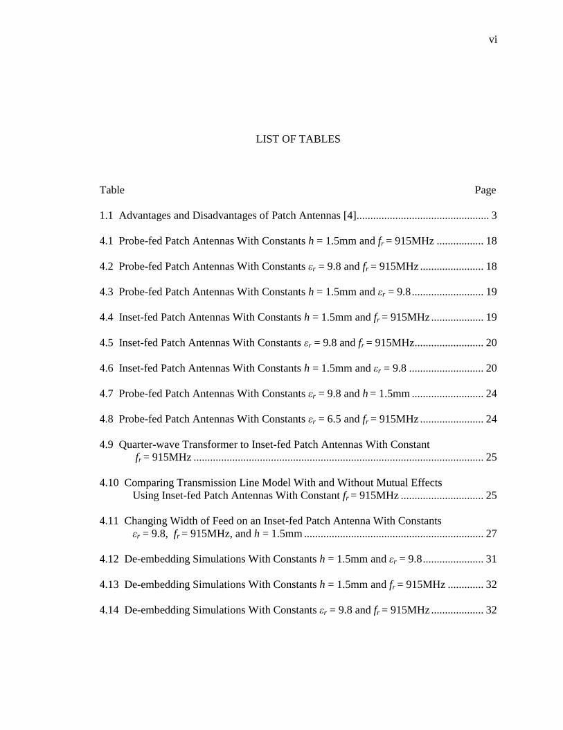
LIST OF TABLES ............................................................................................................. vi
LIST OF FIGURES ......................................................................................................... viii
LIST OF ABBREVIATIONS ............................................................................................ xi
LIST OF SYMBOLS ........................................................................................................ xii
ABSTRACT ..................................................................................................................... xiv
1. INTRODUCTION ......................................................................................................... 1
1.1 Objective of Research ..........................................................................................1
1.2 UHF RFID ............................................................................................................1 1.3 Microstrip Patch Antennas ...................................................................................2
2. PATCH ANTENNA DESIGN ....................................................................................... 4
2.1 Overview of Patch Antenna Design .....................................................................4 2.2 Rectangular Patch Antenna Design ......................................................................5
2.3 Square Patch Antenna Design ..............................................................................6
3. MATCHING TECHNIQUES FOR PATCH ANTENNA DESIGN ............................. 9
3.1 Matching Techniques ...........................................................................................9 3.2 Transmission Line Model ..................................................................................11 3.3 Cavity Model .....................................................................................................12 3.4 Matching By Adjusting the Location of the Feed .............................................13 3.5 Matching With a Quarter-wave Transformer ....................................................14
3.6 Characteristic Impedance of Feeding Transmission Lines ................................14
Page 5
v
Page
4. COMPARISON OF THEORETICAL MODELS ....................................................... 17
4.1 First Set of Simulations ......................................................................................17 4.2 Second Set of Simulations .................................................................................22 4.3 Simulating Slight Changes in the Feeding Transmission Line ..........................26 4.4 A Different Method to Obtain the Edge Zin .......................................................28 4.5 Utilizing the Results From the De-embedding Simulations ..............................33
4.6 Overall Conclusions for Matching a Patch Antenna ..........................................37
5. ELECTROMAGNETIC BAND GAP (EBG) STRUCTURES ................................... 39
5.1 Introducing EBG Structures ...............................................................................39 5.2 Mushroom-like EBG Structures .........................................................................40
5.3 Parametric Study of Mushroom-like EBG Structures .......................................54
6. ANTENNA DESIGNS WITH EBG STRUCTURES ................................................. 57
6.1 EBG Distance From Patch .................................................................................57
6.2 Final Working Design ........................................................................................62
6.3 Similar Research ................................................................................................74
7. CONCLUSIONS.......................................................................................................... 76
BIBLIOGRAPHY ............................................................................................................. 78
APPENDICES
A. OBTAINING WIDTH AND LENGTH OF A SQUARE PATCH ............................ 80
B. OBTAINING THE WIDTH AND GAP OF AN EBG STRUCTURE ....................... 81
Page 6
vi
LIST OF TABLES
Table Page
1.1 Advantages and Disadvantages of Patch Antennas [4] ................................................ 3
4.1 Probe-fed Patch Antennas With Constants h = 1.5mm and fr = 915MHz ................. 18
4.2 Probe-fed Patch Antennas With Constants εr = 9.8 and fr = 915MHz ....................... 18
4.3 Probe-fed Patch Antennas With Constants h = 1.5mm and εr = 9.8 .......................... 19
4.4 Inset-fed Patch Antennas With Constants h = 1.5mm and fr = 915MHz ................... 19
4.5 Inset-fed Patch Antennas With Constants εr = 9.8 and fr = 915MHz ......................... 20
4.6 Inset-fed Patch Antennas With Constants h = 1.5mm and εr = 9.8 ........................... 20
4.7 Probe-fed Patch Antennas With Constants εr = 9.8 and h = 1.5mm .......................... 24
4.8 Probe-fed Patch Antennas With Constants εr = 6.5 and fr = 915MHz ....................... 24
4.9 Quarter-wave Transformer to Inset-fed Patch Antennas With Constant fr = 915MHz ......................................................................................................... 25
4.10 Comparing Transmission Line Model With and Without Mutual Effects Using Inset-fed Patch Antennas With Constant fr = 915MHz .............................. 25
4.11 Changing Width of Feed on an Inset-fed Patch Antenna With Constants
εr = 9.8, fr = 915MHz, and h = 1.5mm ................................................................. 27
4.12 De-embedding Simulations With Constants h = 1.5mm and εr = 9.8 ...................... 31
4.13 De-embedding Simulations With Constants h = 1.5mm and fr = 915MHz ............. 32
4.14 De-embedding Simulations With Constants εr = 9.8 and fr = 915MHz ................... 32
Page 7
vii
Table Page
4.15 Probe-fed Patch Antennas Using De-embedding Results With Constants
h = 1.5mm and fr = 915MHz ................................................................................. 34
4.16 Probe-fed Patch Antennas Using De-embedding Results With Constants
εr = 9.8 and fr = 915MHz ....................................................................................... 34
4.17 Probe-fed Patch Antennas Using De-embedding Results With Constants
h = 1.5mm and εr = 9.8 .......................................................................................... 35
4.18 Inset-fed Patch Antennas Using De-embedding Results With Constants
h = 1.5mm and fr = 915MHz ................................................................................. 35
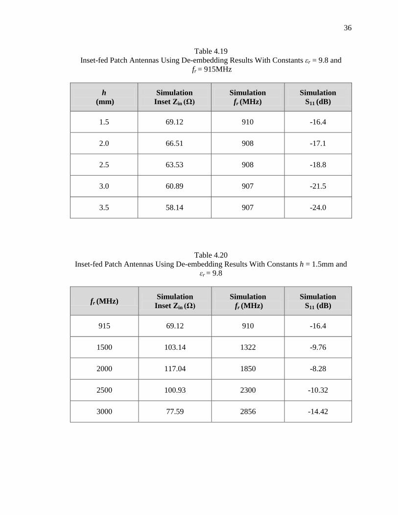
4.19 Inset-fed Patch Antennas Using De-embedding Results With Constants
εr = 9.8 and fr = 915MHz ....................................................................................... 36
4.20 Inset-fed Patch Antennas Using De-embedding Results With Constants
h = 1.5mm and εr = 9.8 .......................................................................................... 36
5.1 Calculated Bandwidth of the Frequency Band Gap ................................................... 43
5.2 Comparison of EBG Simulation Methods ................................................................. 53
5.3 EBG Simulation Times .............................................................................................. 53
6.1 Review of Patch Antenna Design Components ......................................................... 62
6.2 Final Working Design Parameters ............................................................................. 63
6.3 Overall Results of Final Working Design .................................................................. 67
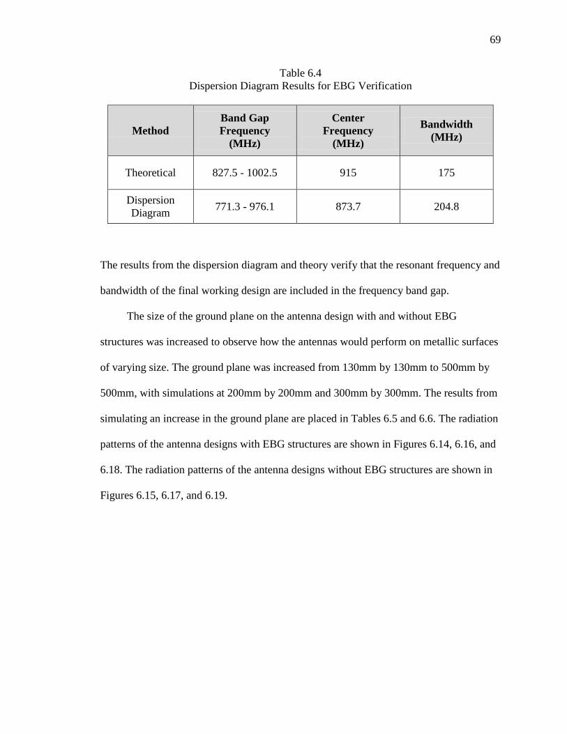
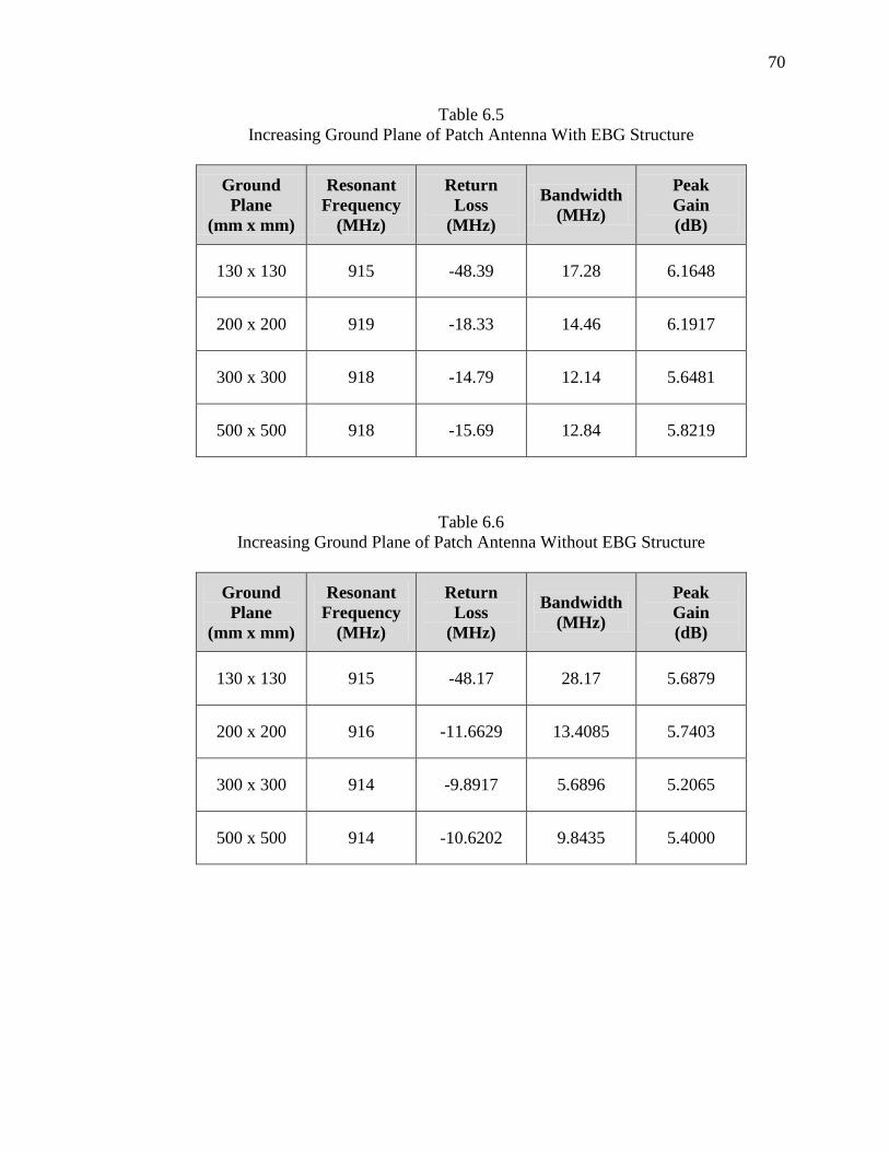
6.4 Dispersion Diagram Results for EBG Verification ................................................... 69
6.5 Increasing Ground Plane of Patch Antenna With EBG Structure ............................. 70
6.6 Increasing Ground Plane of Patch Antenna Without EBG Structure ........................ 70
Page 8
viii
LIST OF FIGURES
Figure Page
2.1 Top View of Patch Antenna ......................................................................................... 4
2.2 Side View of Patch Antenna ........................................................................................ 4
2.3 Patch Length Due to Fringing ...................................................................................... 6
3.1 Probe-fed Patch Antenna ............................................................................................. 9
3.2 Inset-fed Patch Antenna ............................................................................................. 10
3.3 Patch Antenna Fed With a Quarter-wave Transformer ............................................. 10
3.4 Cross-section of a Coaxial Transmission Line .......................................................... 15
4.1 Quarter-wave Transformer Added to Inset-fed Patch Antenna ................................. 23
4.2 De-embedding Inset-fed Patch Antenna in HFSS ..................................................... 28
4.3 Return Loss of De-embedded Inset-fed Patch Antenna With Changing
Characteristic Impedance ...................................................................................... 29
4.4 Return Loss of Quarter-wave Transformer Patch Antenna Designed
Using De-embed Feature ...................................................................................... 30
5.1 Probe-fed Patch Antenna Surrounded by a Mushroom-like EBG Structure [8] ........ 39
5.2 Cross-section of Mushroom-like EBG Structure [8] ................................................. 40
5.3 LC Model of Mushroom-like EBG Structure [8] ...................................................... 40
5.4 Dispersion Diagram of a Mushroom-like EBG Structure [8] .................................... 45
5.5 Brillouin Zone [13] .................................................................................................... 45
Page 9
ix
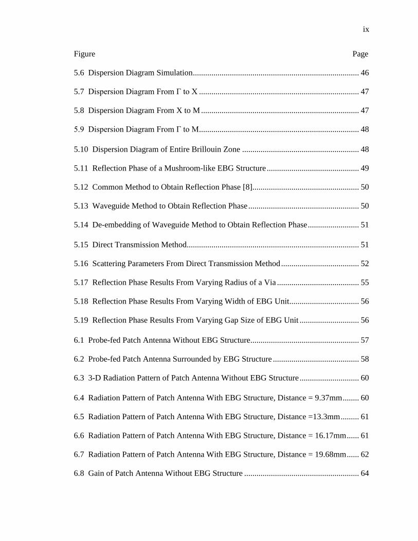
Figure Page
5.6 Dispersion Diagram Simulation ................................................................................. 46
5.7 Dispersion Diagram From Г to X .............................................................................. 47
5.8 Dispersion Diagram From X to M ............................................................................. 47
5.9 Dispersion Diagram From Г to M .............................................................................. 48
5.10 Dispersion Diagram of Entire Brillouin Zone ......................................................... 48
5.11 Reflection Phase of a Mushroom-like EBG Structure ............................................. 49
5.12 Common Method to Obtain Reflection Phase [8].................................................... 50
5.13 Waveguide Method to Obtain Reflection Phase ...................................................... 50
5.14 De-embedding of Waveguide Method to Obtain Reflection Phase ......................... 51
5.15 Direct Transmission Method.................................................................................... 51
5.16 Scattering Parameters From Direct Transmission Method ...................................... 52
5.17 Reflection Phase Results From Varying Radius of a Via ........................................ 55
5.18 Reflection Phase Results From Varying Width of EBG Unit.................................. 56
5.19 Reflection Phase Results From Varying Gap Size of EBG Unit ............................. 56
6.1 Probe-fed Patch Antenna Without EBG Structure..................................................... 57
6.2 Probe-fed Patch Antenna Surrounded by EBG Structure .......................................... 58
6.3 3-D Radiation Pattern of Patch Antenna Without EBG Structure ............................. 60
6.4 Radiation Pattern of Patch Antenna With EBG Structure, Distance = 9.37mm ........ 60
6.5 Radiation Pattern of Patch Antenna With EBG Structure, Distance =13.3mm ......... 61
6.6 Radiation Pattern of Patch Antenna With EBG Structure, Distance = 16.17mm ...... 61
6.7 Radiation Pattern of Patch Antenna With EBG Structure, Distance = 19.68mm ...... 62
6.8 Gain of Patch Antenna Without EBG Structure ........................................................ 64
Page 10
x
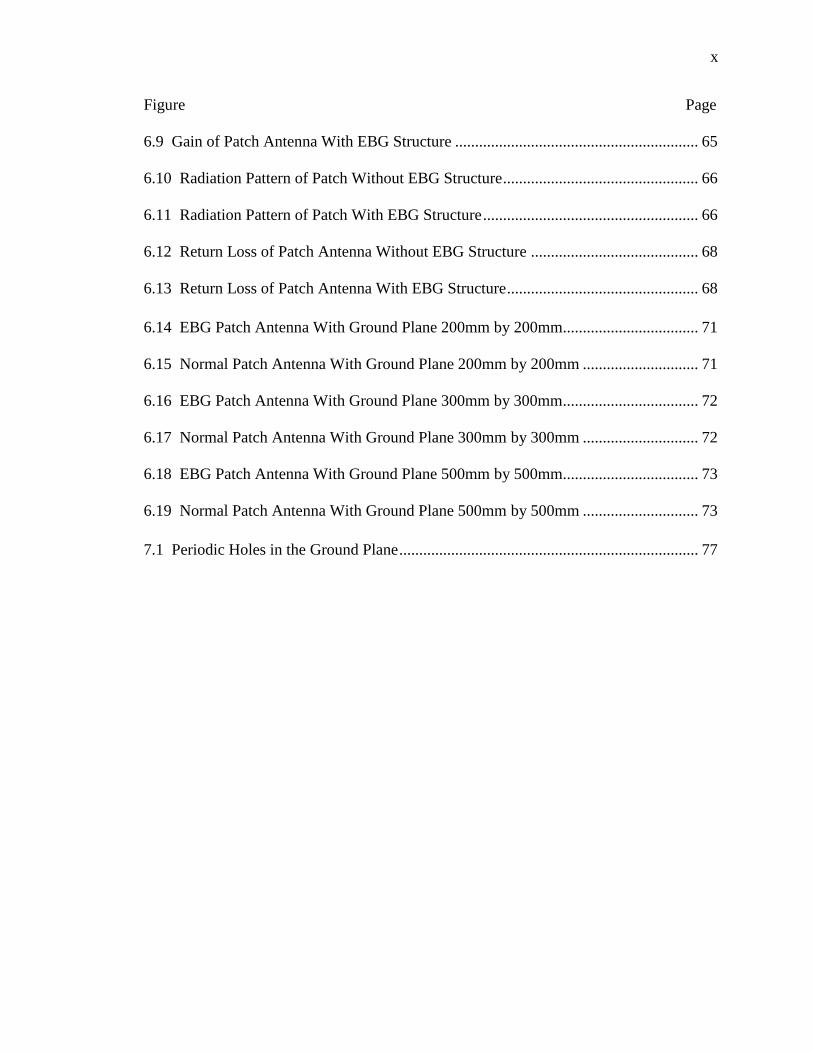
Figure Page
6.9 Gain of Patch Antenna With EBG Structure ............................................................. 65
6.10 Radiation Pattern of Patch Without EBG Structure ................................................. 66
6.11 Radiation Pattern of Patch With EBG Structure ...................................................... 66
6.12 Return Loss of Patch Antenna Without EBG Structure .......................................... 68
6.13 Return Loss of Patch Antenna With EBG Structure ................................................ 68
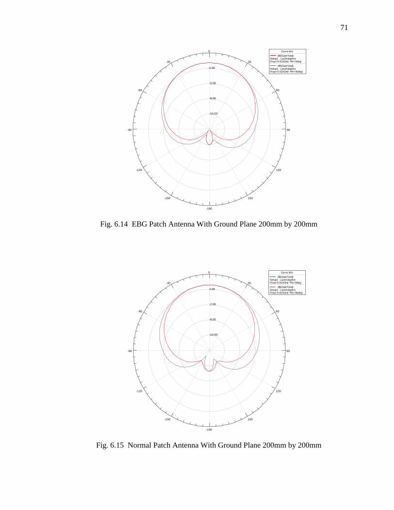
6.14 EBG Patch Antenna With Ground Plane 200mm by 200mm.................................. 71
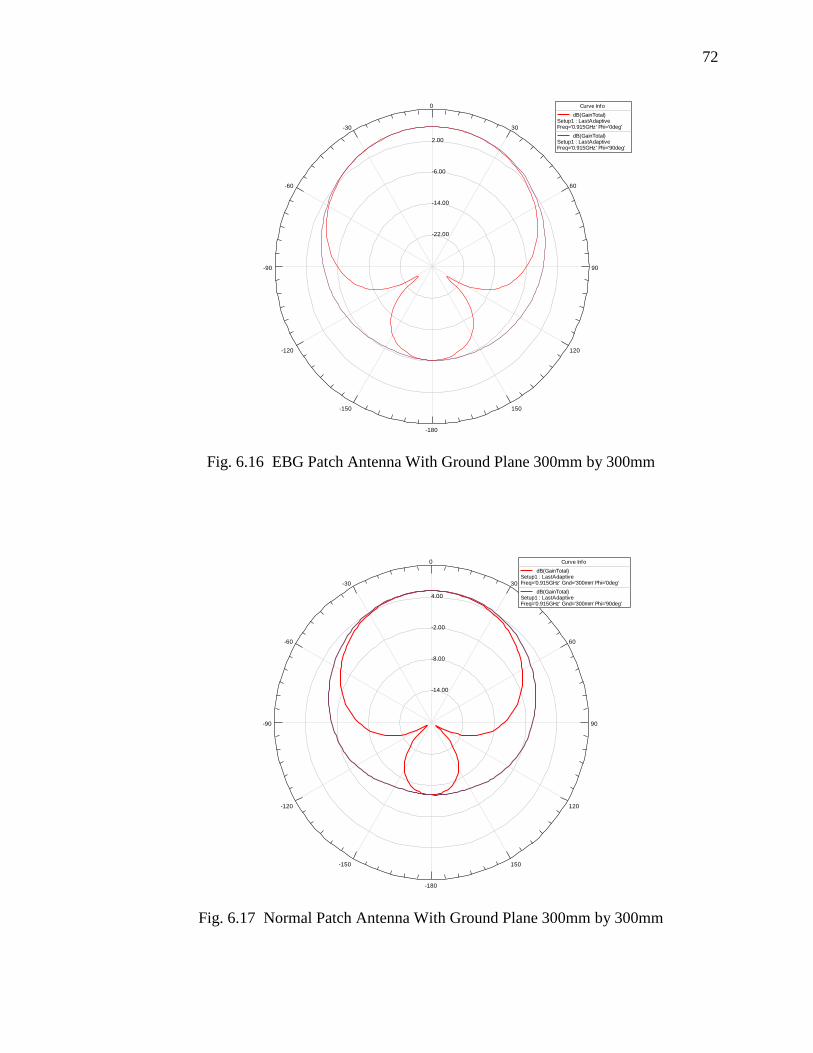
6.15 Normal Patch Antenna With Ground Plane 200mm by 200mm ............................. 71
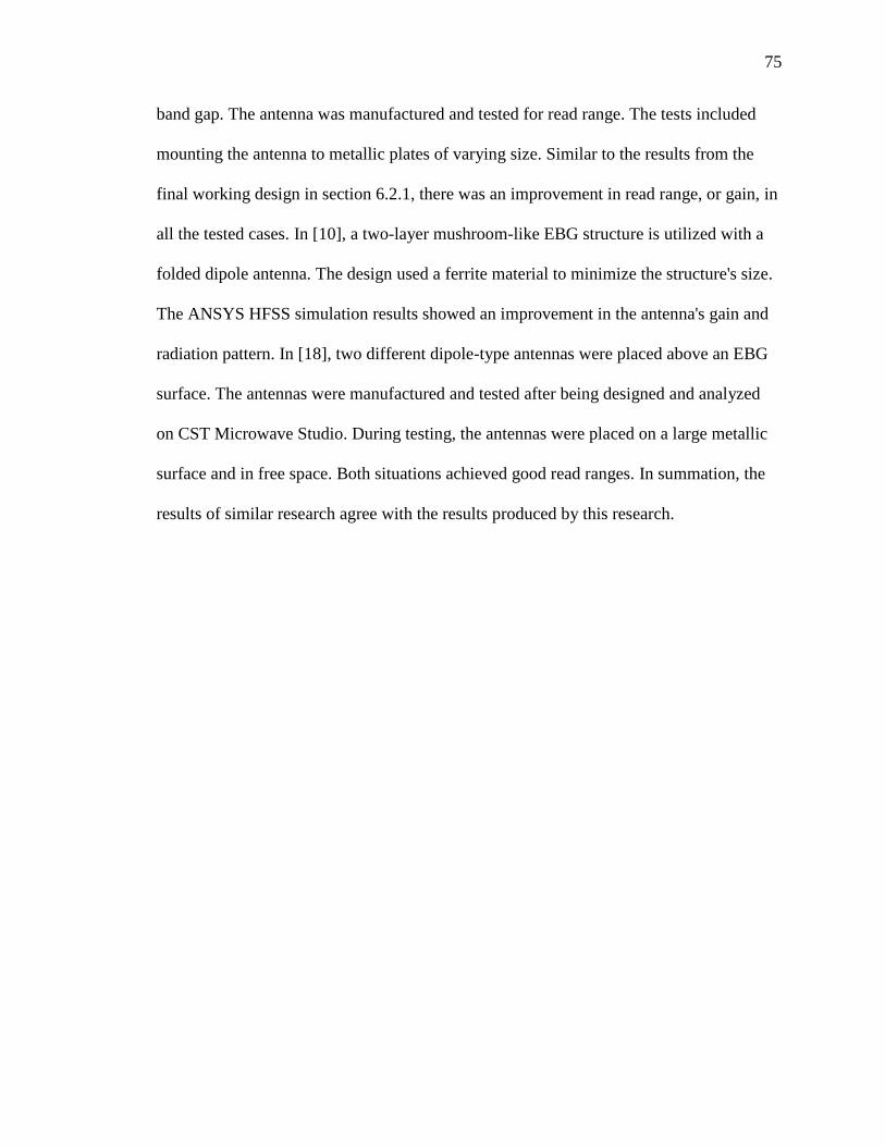
6.16 EBG Patch Antenna With Ground Plane 300mm by 300mm.................................. 72
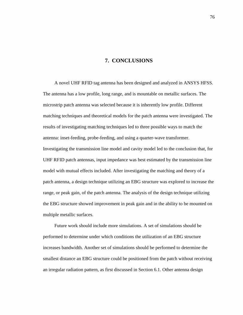
6.17 Normal Patch Antenna With Ground Plane 300mm by 300mm ............................. 72
6.18 EBG Patch Antenna With Ground Plane 500mm by 500mm.................................. 73
6.19 Normal Patch Antenna With Ground Plane 500mm by 500mm ............................. 73
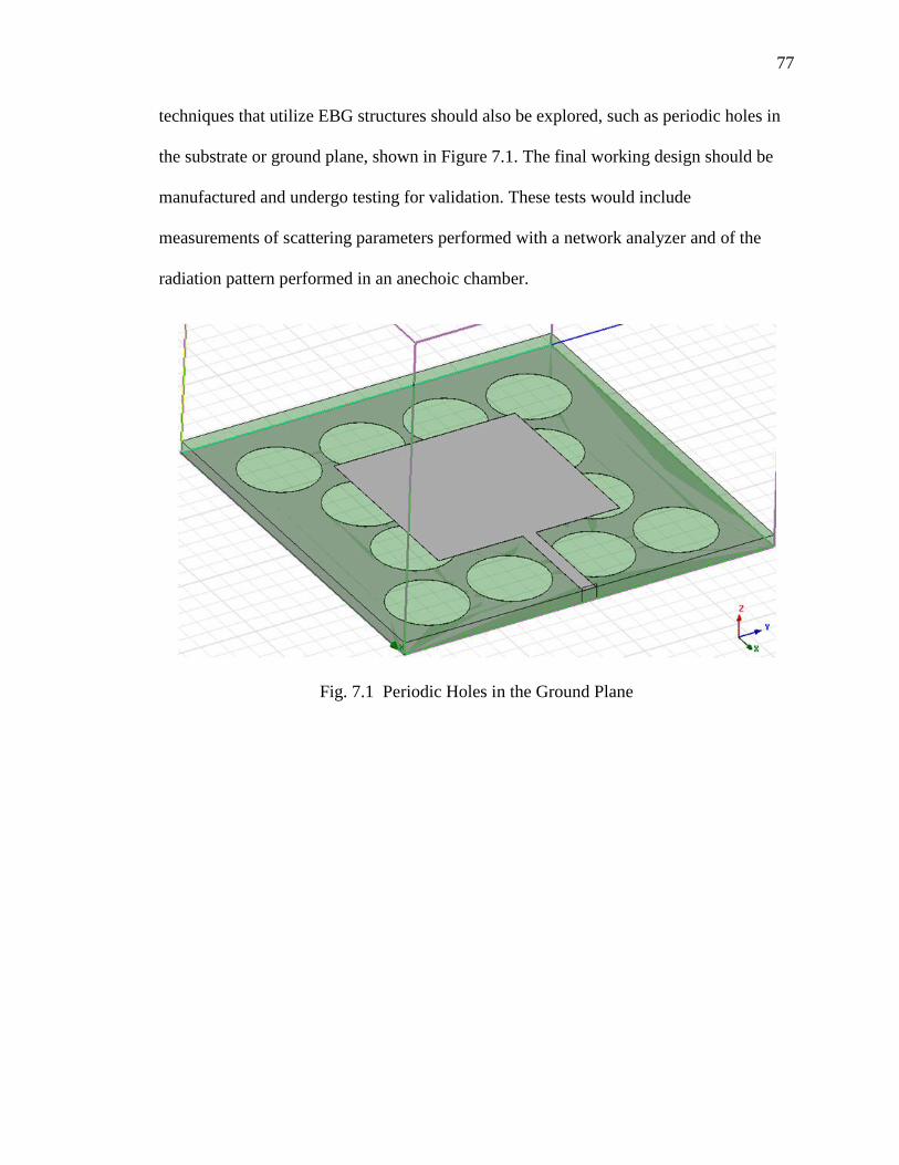
7.1 Periodic Holes in the Ground Plane ........................................................................... 77
Page 11
xi
LIST OF ABBREVIATIONS
UHF Ultra-High Frequency
RFID Radio Frequency Identification
EBG Electromagnetic Band Gap
TL Transmission Line Model
TL-M Transmission Line Model With Mutual Effects
Cav Cavity Model
Cav-M Cavity Model With Mutual Effects
BW Bandwidth
PBC Periodic Boundary Condition
TEM Transverse Electromagnetic
VSWR Voltage Standing Wave Ratio
Page 12
xii
LIST OF SYMBOLS
Wavelength
Resonant Frequency
Dielectric Constant or Relative Permittivity
Height of Substrate
Width of Patch (of EBG Structure)
Length of Patch
Speed of Light in Free Space
Effective Dielectric Constant
Extension Length of Patch Due to Fringing
Conductance of Slot Antenna
Wavelength in Free Space
Wavenumber in Free Space
Admittance of Slot Antenna
Susceptance of Slot Antenna
Input Admittance
Input Impedance
Sine Integral
Page 13
xiii
Mutual Conductance
Bessel Function of First Kind
Inset Distance
Characteristic Impedance of Quarter-wave Transformer
Characteristic Impedance
Load Impedance
Inductance
Capacitance
Permeability
Permittivity
Ω Ohms
Return Loss
Width of EBG unit
Permittivity of Free Space
Length of EBG Gap
Permeability of Free Space
Relative Permeability
Periodic length of EBG
Brillouin Zone Points
Brillouin Zone Wavenumbers
Insertion Loss
Page 14
xiv
ABSTRACT
Reynolds, Nathan D. M.S.E., Purdue University, May 2012. Long Range Ultra-High
Frequency (UHF) Radio Frequency Identification (RFID) Antenna Design. Major
Professor: Abdullah Eroglu.
There is an ever-increasing demand for radio frequency identification (RFID) tags
that are passive, long range, and mountable on multiple surfaces. Currently, RFID
technology is utilized in numerous applications such as supply chain management, access
control, and public transportation. With the combination of sensory systems in recent
years, the applications of RFID technology have been extended beyond tracking and
identifying. This extension includes applications such as environmental monitoring and
healthcare applications. The available sensory systems usually operate in the medium or
high frequency bands and have a low read range. However, the range limitations of these
systems are being overcome by the development of RFID sensors focused on utilizing
tags in the ultra-high frequency (UHF) band.
Generally, RFID tags have to be mounted to the object that is being identified.
Often the objects requiring identification are metallic. The inherent properties of metallic
objects have substantial effects on nearby electromagnetic radiation; therefore, the
operation of the tag antenna is affected when mounted on a metallic surface. This outlines
Page 15
xv
one of the most challenging problems for RFID systems today: the optimization of tag
antenna performance in a complex environment.
In this research, a novel UHF RFID tag antenna, which has a low profile, long
range, and is mountable on metallic surfaces, is designed analytically and simulated using
a 3-D electromagnetic simulator, ANSYS HFSS. A microstrip patch antenna is selected
as the antenna structure, as patch antennas are low profile and suitable for mounting on
metallic surfaces. Matching and theoretical models of the microstrip patch antenna are
investigated. Once matching and theory of a microstrip patch antenna is thoroughly
understood, a unique design technique using electromagnetic band gap (EBG) structures
is explored. This research shows that the utilization of an EBG structure in the patch
antenna design yields an improvement in gain, or range, and in the ability to be mounted
on multiple metallic surfaces.
Page 16
1
1. INTRODUCTION
1.1 Objective of Research
The objective of this research is to design a novel ultra-high frequency (UHF) radio
frequency identification (RFID) tag antenna, which has a low profile, long range, and is
mountable on metallic surfaces. The antenna will be designed on a 3-D electromagnetic
simulator, ANSYS HFSS. Patch antennas are commonly used as UHF RFID tag
antennas. Therefore, the concepts of patch antenna design will be explored. Once the
concepts are understood, different matching techniques and theoretical models will be
investigated. The theoretical models will be compared to determine which model is best
suited for utilization with UHF RFID patch antennas. Once that matching and theory of a
patch antenna are understood, a more unique design technique will be explored: the use
of an electromagnetic band gap (EBG) structure. Throughout the course of research,
specific components of the tag antenna will be established, resulting in a novel design
that has a low profile, long range, and is mountable on metallic surfaces.
1.2 UHF RFID
RFID is a wireless technology that utilizes radio waves to transfer data from a tag
that is designed for tracking and identifying an object. The role of RFID is continuously
expanding and now includes relaying information, as well as other functions. RFID
Page 17
2
technology has helped streamline supply chains by replacing manual systems, such as
barcodes, that were previously used to track shipments and assets. RFID passive tags
designed in the UHF band have been more widely used in the supply chain than tags in
the other frequency bands, due to one major advantage: passive UHF tags have a longer
read range than other passive tags [1]. UHF tags can be read from 3.3m or further, while
low and high frequency tags can only be read from 0.33m and 1m, respectively [1].
However, UHF radio waves reflect off metal and are absorbed by water; therefore, when
UHF RFID systems are positioned in close proximity to metal or water, they do not
function as well as low and high frequency systems [1]. This is one of the main
disadvantages of UHF RFID systems, because RFID tags are commonly required to be
mounted on a variety of metallic surfaces. However, microstrip patch antennas are one of
the types of antennas that are suitable to be mounted on metallic surfaces [2].
UHF is defined as the frequency band from 300MHz to 3GHz. The North
American unlicensed UHF RFID band is from 902MHz to 928MHz. Therefore, an
antenna designed for the UHF RFID band will be resonant at the center frequency of the
UHF RFID band, 915MHz.
1.3 Microstrip Patch Antennas
A microstrip patch antenna, or patch antenna, is a low profile directional antenna
that resonates at a λ/2. The patch antenna consists of a conductive patch of some shape
that is positioned on top of a dielectric substrate. Under the dielectric substrate is
typically a ground plane. The patch antenna radiates normal to the plane of the patch, and
the radiation traveling in the direction of the substrate is reduced by the ground plane [3].
Page 18
3
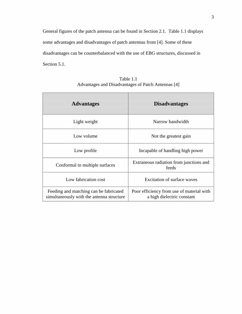
General figures of the patch antenna can be found in Section 2.1. Table 1.1 displays
some advantages and disadvantages of patch antennas from [4]. Some of these
disadvantages can be counterbalanced with the use of EBG structures, discussed in
Section 5.1.
Table 1.1
Advantages and Disadvantages of Patch Antennas [4]
Advantages Disadvantages
Light weight Narrow bandwidth
Low volume Not the greatest gain
Low profile Incapable of handling high power
Conformal to multiple surfaces Extraneous radiation from junctions and
feeds
Low fabrication cost Excitation of surface waves
Feeding and matching can be fabricated
simultaneously with the antenna structure
Poor efficiency from use of material with
a high dielectric constant
Page 19
4
2. PATCH ANTENNA DESIGN
2.1 Overview of Patch Antenna Design
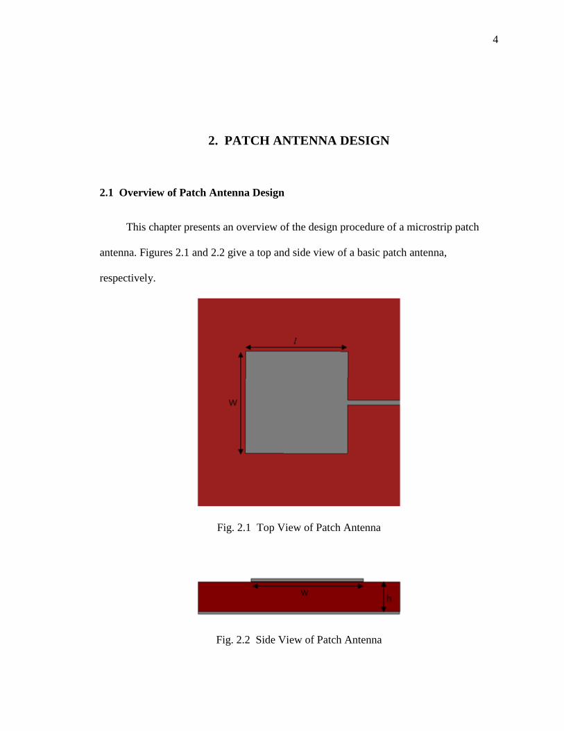
This chapter presents an overview of the design procedure of a microstrip patch
antenna. Figures 2.1 and 2.2 give a top and side view of a basic patch antenna,
respectively.
Fig. 2.1 Top View of Patch Antenna
Fig. 2.2 Side View of Patch Antenna
Page 20
5
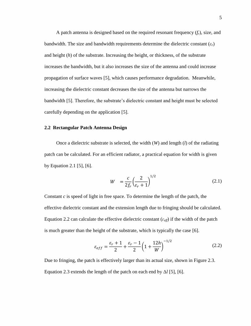
A patch antenna is designed based on the required resonant frequency (fr), size, and
bandwidth. The size and bandwidth requirements determine the dielectric constant (εr)
and height (h) of the substrate. Increasing the height, or thickness, of the substrate
increases the bandwidth, but it also increases the size of the antenna and could increase
propagation of surface waves [5], which causes performance degradation. Meanwhile,
increasing the dielectric constant decreases the size of the antenna but narrows the
bandwidth [5]. Therefore, the substrate’s dielectric constant and height must be selected
carefully depending on the application [5].
2.2 Rectangular Patch Antenna Design
Once a dielectric substrate is selected, the width (W) and length (l) of the radiating
patch can be calculated. For an efficient radiator, a practical equation for width is given
by Equation 2.1 [5], [6].
(2.1)
Constant c is speed of light in free space. To determine the length of the patch, the
effective dielectric constant and the extension length due to fringing should be calculated.
Equation 2.2 can calculate the effective dielectric constant (ɛeff) if the width of the patch
is much greater than the height of the substrate, which is typically the case [6].
(2.2)
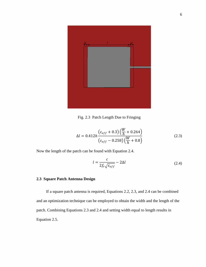
Due to fringing, the patch is effectively larger than its actual size, shown in Figure 2.3.
Equation 2.3 extends the length of the patch on each end by Δl [5], [6].
Page 21
6
Fig. 2.3 Patch Length Due to Fringing
(2.3)
Now the length of the patch can be found with Equation 2.4.
(2.4)
2.3 Square Patch Antenna Design
If a square patch antenna is required, Equations 2.2, 2.3, and 2.4 can be combined
and an optimization technique can be employed to obtain the width and the length of the
patch. Combining Equations 2.3 and 2.4 and setting width equal to length results in
Equation 2.5.
Page 22
7
(2.5)
Equation 2.6 simplifies Equation 2.5 into three functions to make the equation more
manageable.
(2.6)
Expanding Equation 2.6 with Equation 2.2, while changing width to length in Equation
2.2, provides Equation 2.7.
(2.7)
Page 23
8
To obtain the width and length of the patch, graph the right side of Equation 2.7 as a
function of l, and find when it equals zero or utilize another optimization technique.
Another optimization technique can be employed to find the width and length of
the patch by finding the minimum of the absolute value of Equation 2.7. The minimum
value of a function can be found by using an algorithm like the Nelder-Mead algorithm.
The Nelder-Mead algorithm can be utilized in Matlab or Scilab by using the fminsearch
function. To obtain the width and the length of the patch, the fminsearch function has
been used in Scilab, shown in Appendix A.
Page 24
9
3. MATCHING TECHNIQUES FOR PATCH ANTENNA DESIGN
3.1 Matching Techniques
To obtain a desirable return loss at the resonant frequency, a microstrip patch
antenna must be matched to the transmission line feeding it. Two ways to match the patch
antenna to the transmission line will be discussed. The first way to match the patch
antenna to the transmission line is to adjust the location of the feed (y0), as shown in
Figures 3.1 and 3.2. The second way is to use a quarter-wave transformer, as shown in
Figure 3.3.
Fig. 3.1 Probe-fed Patch Antenna
Page 25
10
Fig. 3.2 Inset-fed Patch Antenna
Fig. 3.3 Patch Antenna Fed With a Quarter-wave Transformer
Page 26
11
Before employing any matching technique, the resonant input impedance must be
calculated. The transmission line model and cavity model can be applied to calculate the
input impedance at the edge of the patch antenna. Once the edge input impedance is
calculated, the different matching techniques can be employed.
3.2 Transmission Line Model
In the transmission line model, the patch antenna is viewed as two radiating slots
separated by a low impedance transmission line that is approximately λ/2 in length [6].
To obtain the resonant input impedance, one may start by finding the conductance of one
of these slots. An approximation of the conductance for a slot of finite width may be
used, represented by Equation 3.1 [6].
(3.1)
The variables λ0 and k0 are the wavelength in free space and wavenumber in free space,
respectively.
The input admittance at the first slot can be found by using transmission line theory
to transform the admittance of the second slot to the first slot [6]. Equation 3.2 calculates
the admittances of the slots. If the length of the patch is adjusted for fringing with
Equation 2.3, the distance between the two slots becomes a little less than λ/2 [6]. With
this adjustment in length, the admittance of the second slot becomes its complex
conjugate when it is transformed to the first slot, shown by Equation 3.3[6]. The
transformed susceptance cancels the susceptance of the first slot making the input
admittance real, shown by Equation 3.4 [6].
Page 27
12
(3.2)
(3.3)
(3.4)
This would not be the case if the length was λ/2; the susceptances would add, and the
input admittance would be complex.
Using the input admittance at the first slot, the resonant input impedance at the
edge of the patch is found by Equation 3.5.
(3.5)
Equation 3.5 can be used to approximate the resonant input impedance, but it does not
consider the mutual effects of the two slots. Mutual effects will be taken into account
when using the cavity model.
3.3 Cavity Model
In the cavity model, the patch antenna is viewed as “an array of two radiating
narrow apertures (slots)” separated by a distance of approximately λ/2 [6]. Again, the slot
conductance is first found before the resonant input impedance is obtained. Using the
electric field derived by the cavity model in [5] and [6], the equation for conductance of a
slot is given by Equation 3.6.
(3.6)
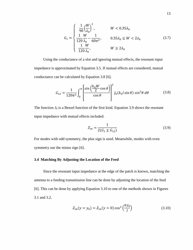
The function Si is the sine integral. Equation 3.7 can approximate this conductance [5].
Page 28
13
(3.7)
Using the conductance of a slot and ignoring mutual effects, the resonant input
impedance is approximated by Equation 3.5. If mutual effects are considered, mutual
conductance can be calculated by Equation 3.8 [6].
(3.8)
The function J0 is a Bessel function of the first kind. Equation 3.9 shows the resonant
input impedance with mutual effects included.
(3.9)
For modes with odd symmetry, the plus sign is used. Meanwhile, modes with even
symmetry use the minus sign [6].
3.4 Matching By Adjusting the Location of the Feed
Since the resonant input impedance at the edge of the patch is known, matching the
antenna to a feeding transmission line can be done by adjusting the location of the feed
[6]. This can be done by applying Equation 3.10 to one of the methods shown in Figures
3.1 and 3.2.
(3.10)
Page 29
14
3.5 Matching With a Quarter-wave Transformer
Another way of matching the antenna to a feeding transmission line is by using a
quarter-wave transformer, shown in Figure 3.3. The quarter-wave transformer is
employed by placing a microstrip transmission line with a length of λ/4 between the
feeding transmission line and the patch antenna. For no reflection, Equation 3.11 shows
the characteristic impedance of the microstrip transmission line with a length of λ/4 [7].
(3.11)
Z0 is the characteristic impedance of the feeding transmission line, and ZL is the resonant
input impedance at the edge of the patch.
3.6 Characteristic Impedance of Feeding Transmission Lines
All patch antenna designs require to be fed in some manner with a feeding
transmission line. Typically, transmission lines are designed to have a characteristic
impedance of 50 ohms. Therefore, all of the antenna designs performed in the following
sections were fed with a transmission line of 50 ohms.
3.6.1 Characteristic impedance of a microstrip transmission line
A microstrip transmission line is used in the feeding of the inset-fed patch antenna
and the patch antenna that is fed by the quarter-wave transformer, shown in Figures 3.2
and 3.3, respectively. Equation 3.12 provides an approximation for the characteristic
impedance of a microstrip transmission line [6], [7].
Page 30
15
(3.12)
The εeff used in Equation 3.12 can be calculated by using Equation 2.2. When calculating
the characteristic impedance of the microstrip transmission line feeding the patch, the W
in Equations 2.2 and 3.12 is the width of the feeding transmission line rather than the
width of the patch.
3.6.2 Characteristic impedance of a coaxial transmission line
A coaxial transmission line is used in the feeding of the probe-fed patch antenna,
shown in Figure 3.1. Figure 3.4 represents the cross-section of a coaxial transmission
line.
Fig. 3.4 Cross-section of a Coaxial Transmission Line
Page 31
16
Typically, the loss of the coaxial transmission line is minuscule and is often not included
in calculations. Therefore, the characteristic impedance of a coaxial transmission line is
given by Equation 3.13 [7].
(3.13)
The inductance can be calculated by using Equation 3.14.
(3.14)
The variable μ is the permeability of the material between the inner and outer conductors.
Meanwhile, the capacitance can be obtained from Equation 3.15.
(3.15)
The variable ɛ is the permittivity of the material between the inner and outer conductors.
Equations 3.13, 3.14, and 3.15 are combined to obtain Equation 3.16.
(3.16)
Simplifying Equation 3.16 creates an equation to quickly approximate the characteristic
impedance of a coaxial transmission line, Equation 3.17.
(3.17)
Page 32
17
4. COMPARISON OF THEORETICAL MODELS
4.1 First Set of Simulations
The cavity and transmission line models were compared in simulations to
determine which one could obtain better matching in a given situation. To obtain
comparable information, patch antennas were designed with either h, εr, or fr being varied
while the other variables were held constant. The majority of the simulations were
designed at the resonant frequency of 915MHz. This is due to the North American
unlicensed UHF RFID band being centered at 915MHz (902MHz – 928MHz). Both
probe-fed and inset-fed patch antennas were simulated using ANSYS HFSS. During the
first and second set of simulations, mutual effects were taken into consideration with the
cavity model but not with the transmission line model.
4.1.1 Simulation results
The following tables show the results of the first set of simulations. Tables 4.1, 4.2,
and 4.3 provide results from probe-fed patch antenna simulations. Tables 4.4, 4.5, and 4.6
provide results from inset-fed patch antenna simulations. Tables 4.1 and 4.4 show results
from simulations that varied the dielectric constant. Tables 4.2 and 4.5 show results from
simulations that varied the height of the substrate. Tables 4.3 and 4.6 show results from
simulations that varied the resonant frequency.
Page 33
18
Table 4.1
Probe-fed Patch Antennas With Constants h = 1.5mm and fr = 915MHz
Calculated edge Zin
(Ω)
Simulation Results
(Trans. Line)
Simulation Results
(Cavity)
εr Trans.
Line Cavity fr (MHz) S11 (dB) fr (MHz) S11 (dB)
6.5 232.4 394.1 885 -7.71 1335 -5.71
8.9 267.0 499.2 900 -8.44 825 -4.66
9.8 278.9 539.0 890 -10.11 860 -4.72
12.9 316.1 675.9 830 -7.45 1500 -9.17
Table 4.2
Probe-fed Patch Antennas With Constants εr = 9.8 and fr = 915MHz
Calculated edge Zin
(Ω)
Simulation Results
(Trans. Line)
Simulation Results
(Cavity)
h (mm) Trans.
Line Cavity fr (MHz) S11 (dB) fr (MHz) S11 (dB)
0.635 278.9 539.1 1275 -8.52 1270 -6.64
1.5 278.9 539.0 890 -10.11 860 -4.72
3.175 278.9 538.4 880 -9.64 850 -5.29
Page 34
19
Table 4.3
Probe-fed Patch Antennas With Constants h = 1.5mm and εr = 9.8
Calculated edge Zin
(Ω)
Simulation Results
(Trans. Line)
Simulation Results
(Cavity)
fr (GHz) Trans.
Line Cavity fr (GHz) S11 (dB) fr (GHz) S11 (dB)
0.915 278.9 539.0 0.890 -10.11 0.860 -4.72
1.5 278.9 539.7 1.455 -25.63 1.320 -7.73
2.5 278.9 537.9 2.395 -17.38 2.375 -14.45
Table 4.4
Inset-fed Patch Antennas With Constants h = 1.5mm and fr = 915MHz
Calculated edge Zin
(Ω)
Simulation Results
(Trans. Line)
Simulation Results
(Cavity)
εr Trans.
Line Cavity fr (MHz) S11 (dB) fr (MHz) S11 (dB)
6.5 232.4 394.1 875 -14.83 870 -9.98
8.9 267.0 499.2 910 -25.19 910 -15.34
9.8 278.9 539.0 910 -26.22 910 -13.82
12.88 316.1 675.9 910 -10.6 910 -11.23
Page 35
20
Table 4.5
Inset-fed Patch Antennas With Constants εr = 9.8 and fr = 915MHz
Calculated edge Zin
(Ω)
Simulation Results
(Trans. Line)
Simulation Results
(Cavity)
h (mm) Trans.
Line Cavity fr (MHz) S11 (dB) fr (MHz) S11 (dB)
0.635 278.9 539.1 910 -7.62 1370 -7.73
1.5 278.9 539.0 910 -26.22 910 -13.82
3.175 278.9 538.4 905 -19.95 855 -15.16
Table 4.6
Inset-fed Patch Antennas With Constants h = 1.5mm and εr = 9.8
Calculated edge Zin
(Ω)
Simulation Results
(Trans. Line)
Simulation Results
(Cavity)
fr (GHz) Trans.
Line Cavity fr (GHz) S11 (dB) fr (GHz) S11 (dB)
0.915 278.9 539.0 0.910 -26.22 0.910 -13.82
1.5 278.9 539.7 1.49 -10.54 1.35 -10.49
2.5 278.9 537.9 2.475 -10.74 2.29 -11.87
Page 36
21
4.1.2 Observations
Looking at the calculations for the edge Zin, both models were minimally affected
by varying the height or resonant frequency, but the results do not confirm this trend. The
results show a significant change in the return loss (S11), signifying a considerable change
in edge Zin. Refer to Tables 4.2, 4.3, 4.5, and 4.6 for the simulation results and
calculations for both models when height and resonant frequency are varied. Anytime the
simulation results for resonant frequency were not close to theoretical expectations, the
results for return loss should be considered irrelevant for comparisons.
In general, the inset-fed patch antennas had a better return loss and were closer to
the expected resonance than the probe-fed patch antennas. The probe-fed patch antennas
trended toward better results as the resonant frequency increased. For both models, the
calculated edge Zin required the antenna to be fed a substantial distance toward the center
of the patch. Equation 3.10 determines the distance from the edge of the patch.
4.1.3 Conclusions
From the observations and results, both models appear to have problems estimating
the edge Zin as can be seen by the high return losses in the tables. Currently, the
transmission line model appears to be more accurate than the cavity model when it comes
to estimating the edge Zin. Since the simulations using the transmission line model had
better results, perhaps adding mutual effects to the transmission line model will increase
its accuracy. The fact that the results were better for the inset-fed patch antennas may
indicate that Equation 3.10 approximates an inset-fed patch antenna better than a probe-
fed patch antenna. For the probe-fed patch antenna, the cavity model may continue its
Page 37
22
trend and obtain better results at higher resonant frequencies, but it is difficult to tell with
the sample size in the first set of simulations. Additional simulations will be needed to
obtain any solid conclusions. Additionally, a quarter-wave transformer could be used to
decrease the required inset distance, possibly enhancing results.
4.2 Second Set of Simulations
The second set of simulations included probe-fed patch antennas that were
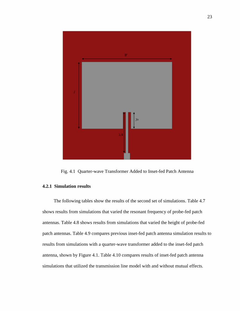
simulated with higher resonant frequencies to determine if the trend of improved return
loss results continued. In addition, probe-fed patch antennas were simulated with varying
heights to determine why the probe-fed patch antenna simulation results from the first set
of simulations were not as ideal as the results from the inset-fed patch antenna
simulations. The simulations also aided in analyzing the effects of varying the height of
the substrate.
Quarter-wave transformers were added to the best matched inset-fed patch antennas
to determine if the decrease in inset distance obtained by Equation 3.10 enhanced the
results. Figure 4.1 shows a model of the quarter-wave transformer added to an inset-fed
patch antenna. Meanwhile, mutual effects were taken into account with the transmission
line model calculations and were compared with the best matched inset-fed patch antenna
simulation results. The mutual effects were included in the transmission line model
calculations by using Equations 3.8 and 3.9.
Page 38
23
Fig. 4.1 Quarter-wave Transformer Added to Inset-fed Patch Antenna
4.2.1 Simulation results
The following tables show the results of the second set of simulations. Table 4.7
shows results from simulations that varied the resonant frequency of probe-fed patch
antennas. Table 4.8 shows results from simulations that varied the height of probe-fed
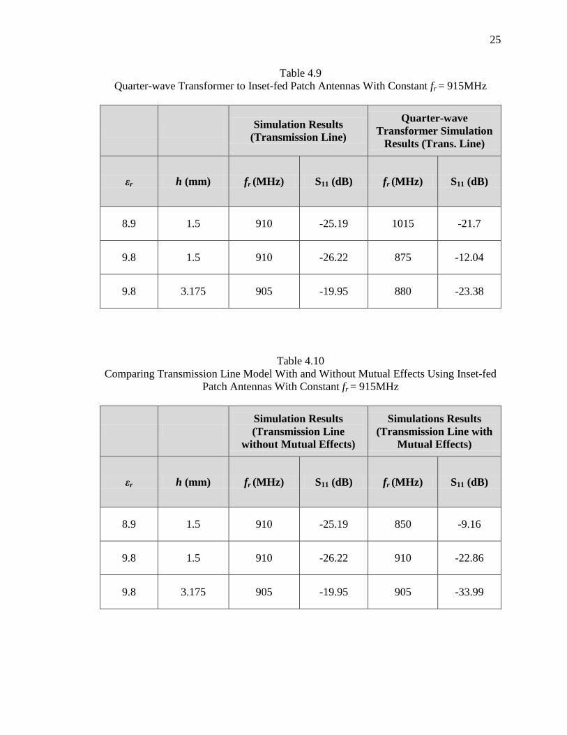
patch antennas. Table 4.9 compares previous inset-fed patch antenna simulation results to
results from simulations with a quarter-wave transformer added to the inset-fed patch
antenna, shown by Figure 4.1. Table 4.10 compares results of inset-fed patch antenna
simulations that utilized the transmission line model with and without mutual effects.
Page 39
24
Table 4.7
Probe-fed Patch Antennas With Constants εr = 9.8 and h = 1.5mm
Simulation Results
(Transmission Line)
Simulation Results
(Cavity)
fr (GHz) fr (GHz) S11 (dB) fr (GHz) S11 (dB)
0.915 0.890 -10.11 0.860 -4.72
1.5 1.455 -25.63 1.320 -7.73
2.5 2.395 -17.38 2.375 -14.45
5 4.665 -28.38 4.645 -9.87
7.5 6.890 -16.48 6.870 -7.32
Table 4.8
Probe-fed Patch Antennas With Constants εr = 6.5 and fr = 915MHz
Simulation Results
(Transmission Line)
Simulation Results
(Cavity)
h (mm) fr (MHz) S11 (dB) fr (MHz) S11 (dB)
1.5 885 -7.71 845 -4.73
3.175 880 -8.06 845 -4.32
5 840 -6.43 835 -3.6
7.5 850 -5.28 830 -3.11
10 830 -4.11 820 -2.55
Page 40
25
Table 4.9
Quarter-wave Transformer to Inset-fed Patch Antennas With Constant fr = 915MHz
Simulation Results
(Transmission Line)
Quarter-wave
Transformer Simulation
Results (Trans. Line)
εr h (mm) fr (MHz) S11 (dB) fr (MHz) S11 (dB)
8.9 1.5 910 -25.19 1015 -21.7
9.8 1.5 910 -26.22 875 -12.04
9.8 3.175 905 -19.95 880 -23.38
Table 4.10
Comparing Transmission Line Model With and Without Mutual Effects Using Inset-fed
Patch Antennas With Constant fr = 915MHz
Simulation Results
(Transmission Line
without Mutual Effects)
Simulations Results
(Transmission Line with
Mutual Effects)
εr h (mm) fr (MHz) S11 (dB) fr (MHz) S11 (dB)
8.9 1.5 910 -25.19 850 -9.16
9.8 1.5 910 -26.22 910 -22.86
9.8 3.175 905 -19.95 905 -33.99
Page 41
26
4.2.2 Observations
The probe-fed patch antenna simulations using the transmission line model
provided better return loss than the cavity model for all frequencies and heights, shown in
Tables 4.7 and 4.8. Table 4.8 also shows that for both of the theoretical models,
increasing the height of the substrate increased the return loss and the resonant frequency
was further from theory. Using the quarter-wave transformer before inset-feeding the
patch did not produce better results, shown in Table 4.9. The results for the transmission
line model with and without mutual effects included were highly varied and inconclusive,
shown in Table 4.10.
4.2.3 Conclusions
Looking at the first two sets of simulations, the transmission line model appears to
be a more ideal model than the cavity model for estimating the edge Zin. The quarter-
wave transformer added to the inset-fed patch antenna will not be pursued, as results do
not appear to be an improvement upon the normal inset-fed patch antenna. It will require
more simulations to determine whether the transmission line model should include
mutual effects.
4.3 Simulating Slight Changes in the Feeding Transmission Line
When changing the dielectric constant of the substrate, height of the substrate, or
both, a new feeding microstrip transmission line must be calculated. These new estimates
could produce slightly different characteristic impedances than other feeding lines for
Page 42
27
other patch antennas. Therefore, simulations of feed lines with slightly different
characteristic impedances are needed.
4.3.1 Simulation results
Inset-fed patch antenna simulations were performed while varying the feeding
microstrip transmission line width; Table 4.11 displays the results.
Table 4.11
Changing Width of Feed on an Inset-fed Patch Antenna With Constants εr = 9.8,
fr = 915MHz, and h = 1.5mm
Feed width (mm) Calculated Z0 fr (MHz) S11 (dB)
1.460 49.85 855 -16.07
1.462 49.83 910 -36.14
1.463 49.81 910 -35.53
1.464 49.79 910 -23.77
4.3.2 Observations and conclusions
The characteristic impedances of the feeding transmission lines are approximately
the same, yet there was wide disparity between a feed width of 1.460mm and those with a
width of 1.462mm to 1.464mm. Therefore, the differences in the results of the first two
sets of simulations could partially be from the error that occurs when transmission lines
Page 43
28
with slightly different characteristic impedances are used. This problem highlights a need
to find another method to compare the transmission line and cavity models.
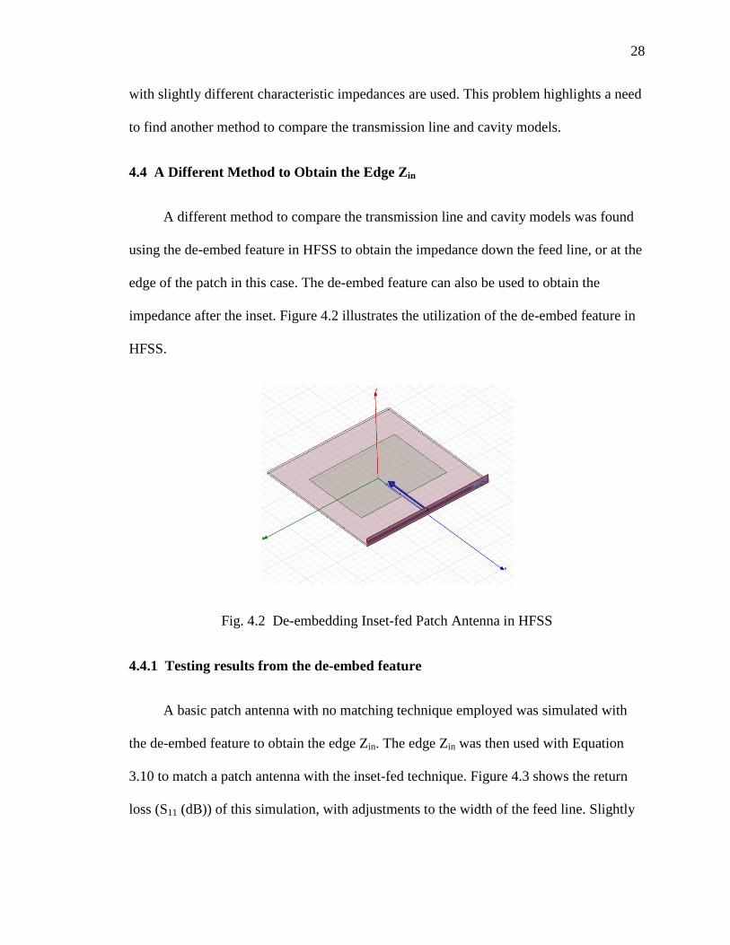
4.4 A Different Method to Obtain the Edge Zin
A different method to compare the transmission line and cavity models was found
using the de-embed feature in HFSS to obtain the impedance down the feed line, or at the
edge of the patch in this case. The de-embed feature can also be used to obtain the
impedance after the inset. Figure 4.2 illustrates the utilization of the de-embed feature in
HFSS.
Fig. 4.2 De-embedding Inset-fed Patch Antenna in HFSS
4.4.1 Testing results from the de-embed feature
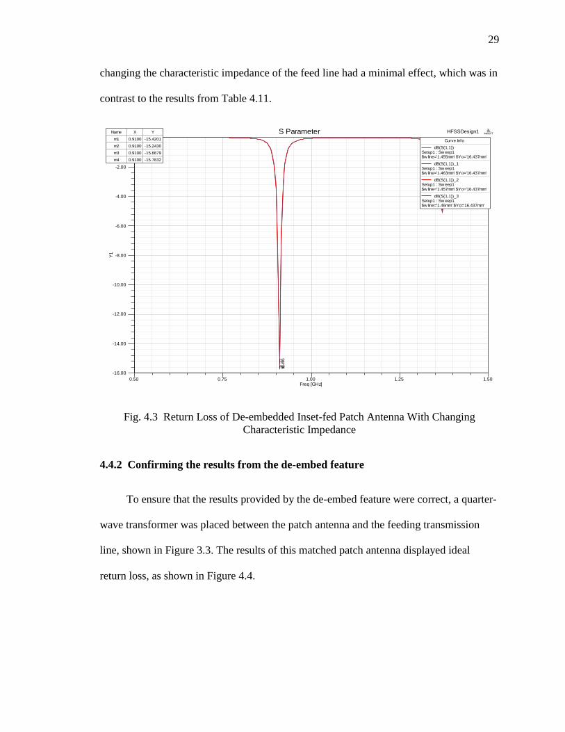
A basic patch antenna with no matching technique employed was simulated with
the de-embed feature to obtain the edge Zin. The edge Zin was then used with Equation
3.10 to match a patch antenna with the inset-fed technique. Figure 4.3 shows the return
loss (S11 (dB)) of this simulation, with adjustments to the width of the feed line. Slightly
Page 44
29
changing the characteristic impedance of the feed line had a minimal effect, which was in
contrast to the results from Table 4.11.
Fig. 4.3 Return Loss of De-embedded Inset-fed Patch Antenna With Changing
Characteristic Impedance
4.4.2 Confirming the results from the de-embed feature
To ensure that the results provided by the de-embed feature were correct, a quarter-
wave transformer was placed between the patch antenna and the feeding transmission
line, shown in Figure 3.3. The results of this matched patch antenna displayed ideal
return loss, as shown in Figure 4.4.
0.50 0.75 1.00 1.25 1.50Freq [GHz]
-16.00
-14.00
-12.00
-10.00
-8.00
-6.00
-4.00
-2.00
0.00
Y1
Ansoft LLC HFSSDesign1S Parameter ANSOFT
m1m2
m3m4
Curve Info
dB(S(1,1))Setup1 : Sw eep1$w line='1.455mm' $Yo='16.437mm'
dB(S(1,1))_1Setup1 : Sw eep1$w line='1.463mm' $Yo='16.437mm'
dB(S(1,1))_2Setup1 : Sw eep1$w line='1.457mm' $Yo='16.437mm'
dB(S(1,1))_3Setup1 : Sw eep1$w line='1.46mm' $Yo='16.437mm'
Name X Y
m1 0.9100 -15.4201
m2 0.9100 -15.2430
m3 0.9100 -15.6679
m4 0.9100 -15.7632
Page 45
30
Fig. 4.4 Return Loss of Quarter-wave Transformer Patch Antenna Designed Using
De-embed Feature
4.4.3 De-embedding simulations of an unmatched patch antenna
Basic patch antennas with no matching technique employed were simulated with
the de-embed feature to obtain the edge Zin. The results were compared to the calculated
edge Zin of the transmission line model with and without mutual effects, and the cavity
model with and without mutual effects.
0.80 0.83 0.85 0.88 0.90 0.93 0.95 0.98 1.00 1.03Freq [GHz]
-60.00
-50.00
-40.00
-30.00
-20.00
-10.00
0.00
dB
(S(1
,1))
Ansoft LLC HFSSDesign1XY Plot 2 ANSOFT
m1
Curve Info
dB(S(1,1))Setup1 : Sw eep1
Name X Y
m1 0.9000 -56.1256
Page 46
31
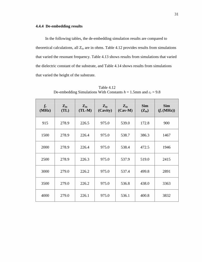
4.4.4 De-embedding results
In the following tables, the de-embedding simulation results are compared to
theoretical calculations, all Zin are in ohms. Table 4.12 provides results from simulations
that varied the resonant frequency. Table 4.13 shows results from simulations that varied
the dielectric constant of the substrate, and Table 4.14 shows results from simulations
that varied the height of the substrate.
Table 4.12
De-embedding Simulations With Constants h = 1.5mm and εr = 9.8
fr
(MHz)
Zin
(TL)
Zin
(TL-M)
Zin
(Cavity)
Zin
(Cav-M)
Sim
(Zin)
Sim
(fr (MHz))
915 278.9 226.5 975.0 539.0 172.8 900
1500 278.9 226.4 975.0 538.7 386.3 1467
2000 278.9 226.4 975.0 538.4 472.5 1946
2500 278.9 226.3 975.0 537.9 519.0 2415
3000 279.0 226.2 975.0 537.4 499.8 2891
3500 279.0 226.2 975.0 536.8 438.0 3363
4000 279.0 226.1 975.0 536.1 400.8 3832
Page 47
32
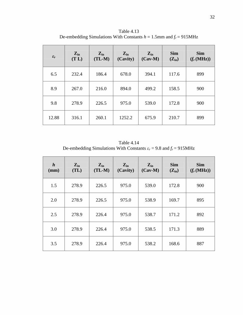
Table 4.13
De-embedding Simulations With Constants h = 1.5mm and fr = 915MHz
εr Zin
(T L)
Zin
(TL-M)
Zin
(Cavity)
Zin
(Cav-M)
Sim
(Zin)
Sim
(fr (MHz))
6.5 232.4 186.4 678.0 394.1 117.6 899
8.9 267.0 216.0 894.0 499.2 158.5 900
9.8 278.9 226.5 975.0 539.0 172.8 900
12.88 316.1 260.1 1252.2 675.9 210.7 899
Table 4.14
De-embedding Simulations With Constants εr = 9.8 and fr = 915MHz
h
(mm)
Zin
(TL)
Zin
(TL-M)
Zin
(Cavity)
Zin
(Cav-M)
Sim
(Zin)
Sim
(fr (MHz))
1.5 278.9 226.5 975.0 539.0 172.8 900
2.0 278.9 226.5 975.0 538.9 169.7 895
2.5 278.9 226.4 975.0 538.7 171.2 892
3.0 278.9 226.4 975.0 538.5 171.3 889
3.5 278.9 226.4 975.0 538.2 168.6 887
Page 48
33
4.4.5 Observations and conclusions from de-embedding results
Changing the height of the substrate had minimal effect on the input impedance just
as the two different theoretical models suggested, contrary to the observations in the first
set of equations. At the resonant frequency of 915MHz, the transmission line model with
mutual effects included was the best estimate of the edge Zin. As the resonant frequency
rose, the edge Zin was better estimated by the cavity model with mutual effects included,
which was unexpected based upon previous results.
4.5 Utilizing the Results From the De-embedding Simulations
After obtaining the edge Zin, the de-embedding simulation results were utilized to
test the accuracy of Equation 3.10 for inset-fed and probe-fed patch antennas. As done in
previous sections, patch antennas were designed with either h, εr, or fr being varied while
the other variables were held constant.
4.5.1 Results after applying Equation 3.10
The following tables provide the results of the simulations performed to test the
accuracy of Equation 3.10. Tables 4.15, 4.16, and 4.17 provide results from probe-fed
patch antenna simulations. Tables 4.18, 4.19, and 4.20 provide results from inset-fed
patch antenna simulations. Tables 4.15 and 4.18 show results from simulations that
varied the dielectric constant of the substrate. Tables 4.16 and 4.19 show results from
simulations that varied the height of the substrate. Tables 4.17 and 4.20 show results from
simulations that varied the resonant frequency.
Page 49
34
Table 4.15
Probe-fed Patch Antennas Using De-embedding Results With Constants h = 1.5mm and
fr = 915MHz
εr Simulation
Inset Zin (Ω)
Simulation
fr (MHz)
Simulation
S11 (dB)
6.5 43.59 899 -23.11
8.9 42.69 900 -21.16
9.8 42.41 899 -20.84
12.88 42.25 894 -21.31
Table 4.16
Probe-fed Patch Antennas Using De-embedding Results With Constants εr = 9.8 and
fr = 915MHz
h (mm) Simulation
Inset Zin (Ω)
Simulation
fr (MHz)
Simulation
S11 (dB)
1.5 42.41 899 -20.84
2.0 43.79 894 -22.66
2.5 43.58 890 -22.37
3.0 43.39 886 -21.53
3.5 43.79 884 -21.28
Page 50
35
Table 4.17
Probe-fed Patch Antennas Using De-embedding Results With Constants h = 1.5mm and
εr = 9.8
fr (MHz) Simulation
Inset Zin (Ω)
Simulation
fr (MHz)
Simulation
S11 (dB)
915 42.41 899 -20.84
1500 40.42 1438 -19.42
2000 39.39 1917 -18.38
2500 35.38 2378 -15.23
3000 34.00 2836 -14.35
Table 4.18
Inset-fed Patch Antennas Using De-embedding Results With Constants h = 1.5mm and
fr = 915MHz
εr Simulation
Inset Zin (Ω)
Simulation
fr (MHz)
Simulation
S11 (dB)
6.5 54.36 885 -29.7
8.9 69.09 886 -16.1
9.8 69.12 910 -16.4
12.88 89.78 883 -10.9
Page 51
36
Table 4.19
Inset-fed Patch Antennas Using De-embedding Results With Constants εr = 9.8 and
fr = 915MHz
h
(mm)
Simulation
Inset Zin (Ω)
Simulation
fr (MHz)
Simulation
S11 (dB)
1.5 69.12 910 -16.4
2.0 66.51 908 -17.1
2.5 63.53 908 -18.8
3.0 60.89 907 -21.5
3.5 58.14 907 -24.0
Table 4.20
Inset-fed Patch Antennas Using De-embedding Results With Constants h = 1.5mm and
εr = 9.8
fr (MHz) Simulation
Inset Zin (Ω)
Simulation
fr (MHz)
Simulation
S11 (dB)
915 69.12 910 -16.4
1500 103.14 1322 -9.76
2000 117.04 1850 -8.28
2500 100.93 2300 -10.32
3000 77.59 2856 -14.42
Page 52
37
4.5.2 Observations
With a few exceptions, the return loss of the results was better than the return loss
of the results from the first set of simulations. Looking at Tables 4.17 and 4.20, the
probe-fed patch antenna simulations had much better return loss results than the inset-fed
patch antenna simulations as resonant frequency was varied, despite the return loss
results from the probe-fed patch antenna simulations continuously getting worse as
resonant frequency was increased.
4.5.3 Conclusions
For most cases, Equation 3.10 is fairly accurate with either the probe-fed or the
inset-fed technique being applied. The results after applying Equation 3.10 to higher
resonant frequency patch antennas are inconclusive, but for the resonant frequency of
interest (915MHz), the results show that Equation 3.10 provides a good estimate for the
inset distance.
4.6 Overall Conclusions for Matching a Patch Antenna
For the resonant frequency of 915MHz, the transmission line model with mutual
effects included is the best estimate of the edge Zin. As shown in Tables 4.13 and 4.14,
the calculations for the edge Zin of the transmission line model with mutual effects
included were closest to the simulation results. Therefore, the designs in future chapters
utilize the transmission line model with mutual effects included to estimate the edge Zin.
Meanwhile, the cavity model with mutual effects included is the best estimate for the
edge Zin when the resonant frequency is increased to 2GHz or higher, shown by Table
Page 53
38
4.12. In most cases, Equation 3.10 is a relatively accurate method for estimating the inset
distance, shown in Section 4.5.1. Also shown in Section 4.5.1, both inset-fed and probe-
fed patch antennas are appropriate to use with Equation 3.10, especially at the resonant
frequency of 915MHz. Therefore, future chapter designs utilize Equation 3.10 to estimate
the inset distance whether the inset-fed or the probe-fed technique is employed.
Page 54
39
5. ELECTROMAGNETIC BAND GAP (EBG) STRUCTURES
5.1 Introducing EBG Structures
Since the design of a patch antenna and ways of matching a patch antenna have
been covered, more unique design techniques may now be explored. One way to increase
the gain, or range, of a patch antenna is the utilization of EBG structures. EBG structures
are periodic structures that reduce the propagation of surface waves. The reduction of
surface waves increases antenna gain; minimizes the back lobe, which increases
directivity; and increases bandwidth [8]. The EBG structure that will be investigated is
the mushroom-like EBG structure, which was developed by Sievenpiper in [9]. The
effects of a mushroom-like EBG structure will be analyzed by surrounding a UHF RFID
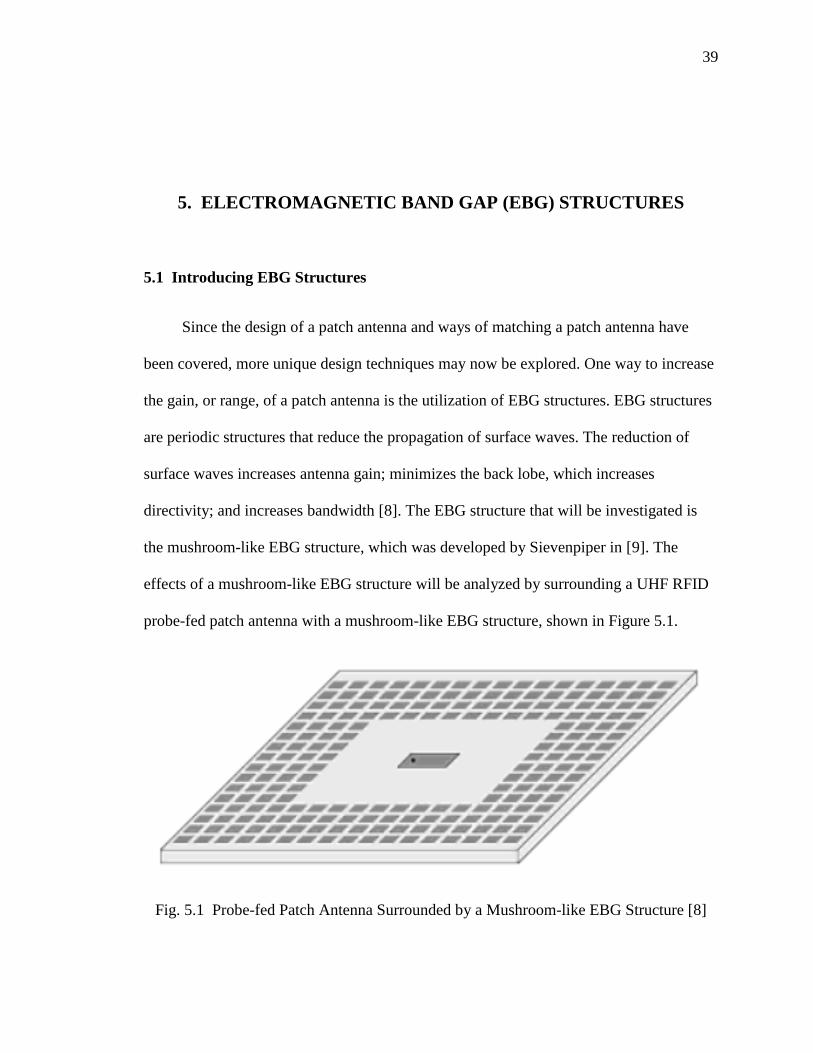
probe-fed patch antenna with a mushroom-like EBG structure, shown in Figure 5.1.
Fig. 5.1 Probe-fed Patch Antenna Surrounded by a Mushroom-like EBG Structure [8]
Page 55
40
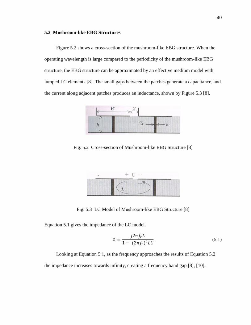
5.2 Mushroom-like EBG Structures
Figure 5.2 shows a cross-section of the mushroom-like EBG structure. When the
operating wavelength is large compared to the periodicity of the mushroom-like EBG
structure, the EBG structure can be approximated by an effective medium model with
lumped LC elements [8]. The small gaps between the patches generate a capacitance, and
the current along adjacent patches produces an inductance, shown by Figure 5.3 [8].
Fig. 5.2 Cross-section of Mushroom-like EBG Structure [8]
Fig. 5.3 LC Model of Mushroom-like EBG Structure [8]
Equation 5.1 gives the impedance of the LC model.
(5.1)
Looking at Equation 5.1, as the frequency approaches the results of Equation 5.2
the impedance increases towards infinity, creating a frequency band gap [8], [10].
Page 56
41
(5.2)
Equation 5.3 provides the capacitance for the LC model.
(5.3)
Meanwhile, Equation 5.4 calculates the inductance for the LC model.
μ (5.4)
The constants ɛ0 and μ0 are the permittivity of free space and the permeability of free
space, respectively. The variable μr is the relative permeability of the substrate. By
combining Equations 5.2, 5.3, and 5.4, Equation 5.5 is obtained.
(5.5)
Separating the known values from the unknown variables results in Equation 5.6.
(5.6)
Knowing the approximate size that is allotted for the EBG structure, the width (w) of the
square mushroom top can be selected, and the size of the gap (g) can be found through
Equation 5.7.
(5.7)
The structure can also be designed based on its periodic length (a), given in Equation 5.8.
(5.8)
Using Equations 5.6 and 5.8, Equation 5.9 is obtained.
Page 57
42
(5.9)
If a periodic length has been determined, the length of the EBG structure's gap can be
obtained by using Equation 5.9 and an optimization technique. After the length of the gap
is obtained, the width of the EBG structure is easily computed with Equation 5.8. One
optimization technique used in conjunction with Equation 5.9 to obtain the size of the gap
has been performed in Scilab, located in Appendix B.
For a frequency band gap centered at 915MHz, a patch antenna surrounded by a
mushroom-like EBG structure on a typical substrate would either require gaps that are
too small to manufacture, or the antenna structure would be unreasonably large. To
maintain a reasonably sized structure, either a dielectric with a really high permittivity
must be used or a ferrite material as suggested in [10]. The ferrite material uses a µr ≠ 1,
which requires a completely new set of equations for the patch antenna. Therefore, a
ferrite material will not be used in designs in future sections. In general, a relative
permittivity greater than 20 may be considered really high. However, materials with a
relative permittivity around 10, still considered high, are more readily available and will
therefore be used to obtain a relatively reasonable structure size.
As seen in Equation 5.3, using a higher permittivity increases the capacitance. This
increase in capacitance decreases the bandwidth of the frequency band gap, whereas if µr
is increased the inductance increases, according to Equation 5.4. This increase in
inductance increases the bandwidth of the frequency band gap. This is one of the main
reasons the ferrite material is suggested in [10]. Equation 5.10 shows the relationship
between the bandwidth of the frequency band gap and the lumped LC elements [10].
Page 58
43
(5.10)
Using the inductance and capacitance found in Equations 5.3 and 5.4, an approximation
for the bandwidth of the frequency band gap can be obtained by Equation 5.11.
(5.11)
Table 5.1 includes calculations for the bandwidth of a frequency band gap designed to be
centered at 915MHz, utilizing Equation 5.11 and possible substrates for future designs.
Table 5.1
Calculated Bandwidth of the Frequency Band Gap
εr h
(mm)
Calculated
Bandwidth
(MHz)
9.8 3 52.57
9.8 5 87.61
9.8 10 175.23
10.2 3 52.57
10.2 5 87.61
10.2 10 175.23
As shown in Table 5.1, the lower amount of bandwidth resulting from the use of a high
permittivity dielectric opposed to the use of ferrite material is not an issue for designs in
Page 59
44
future sections, considering that the UHF RFID band is only 26 MHz. Table 5.1 also
illustrates that the height of the substrate determines the bandwidth, and changing the
dielectric constant has no effect. This is because the inductance of the LC model is
dependent on only the height of the dielectric, shown in Equation 5.4. Since inductance is
unchangeable by adjusting the width or gap of the EBG structure, to have the band gap
centered at the given resonant frequency, the capacitance is dependent on the inductance,
shown by Equation 5.2. Therefore, the height of the dielectric substrate determines both
the inductance and the capacitance of the LC model at a given resonant frequency. Since
the height of the dielectric substrate determines both the inductance and the capacitance,
the bandwidth is dependent only upon the height of the dielectric substrate at a given
resonant frequency, shown by Equation 5.11.
5.2.1 Dispersion diagram method
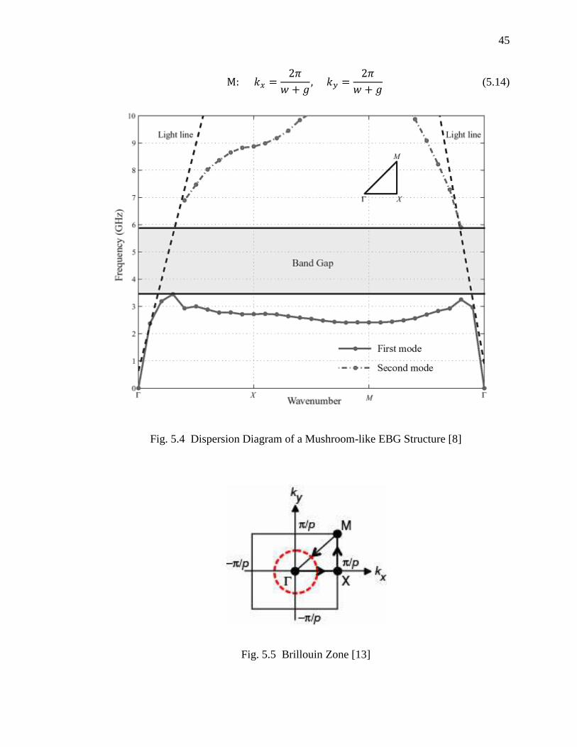
One approach to obtaining the frequency of the surface wave band gap is to
generate a dispersion diagram, shown in Figure 5.4. The use of dispersion diagrams in
locating the frequency band gap is demonstrated in [8], [11], and [12]. The dispersion
diagram focuses upon the Brillouin zone, which is essential to characterizing periodic
structures. Since EBG structures are periodic, all the attributes corresponding with wave-
propagation can be obtained by examining the Brillouin zone [13]. Figure 5.5 illustrates
the Brillouin zone. Equations 5.12, 5.13, and 5.14 define the Brillouin zone points.
(5.12)
(5.13)
Page 60
45
(5.14)
Fig. 5.4 Dispersion Diagram of a Mushroom-like EBG Structure [8]
Fig. 5.5 Brillouin Zone [13]
Page 61
46
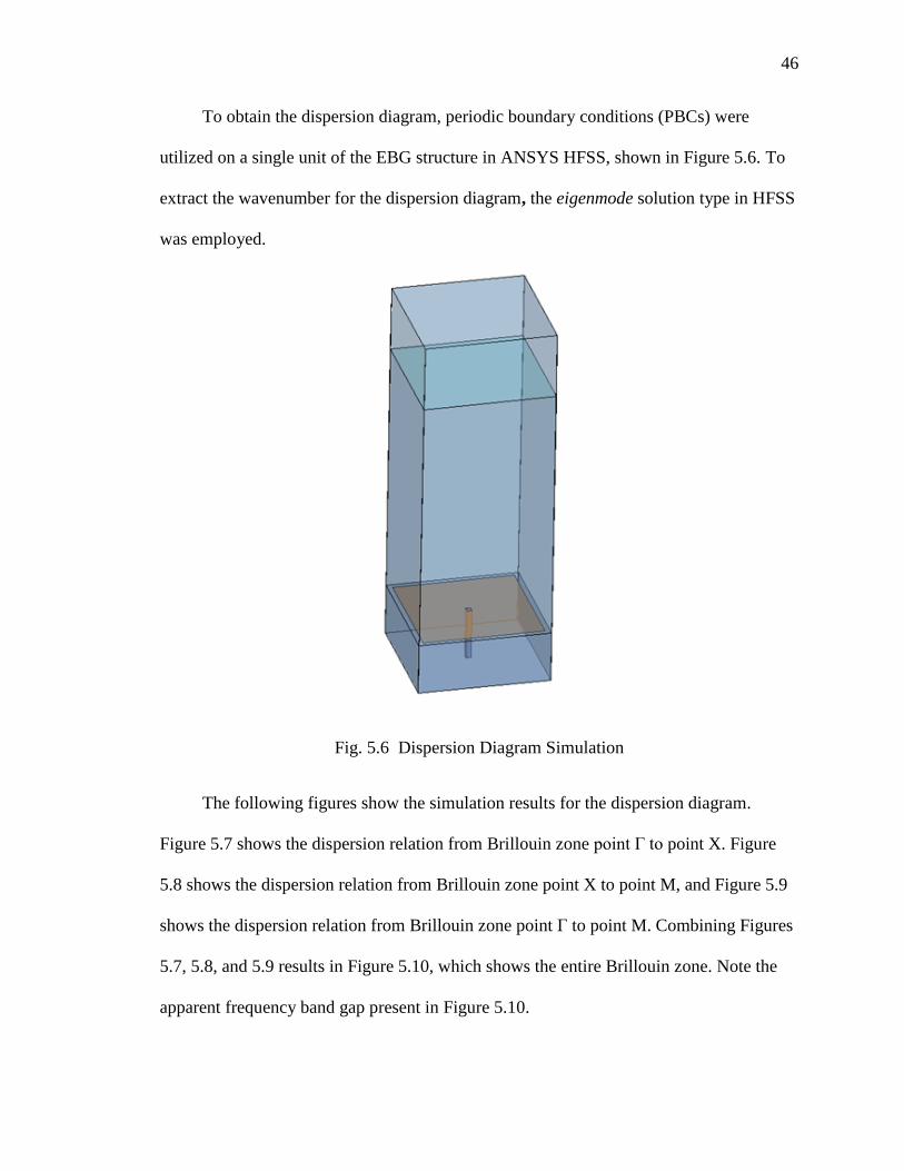
To obtain the dispersion diagram, periodic boundary conditions (PBCs) were
utilized on a single unit of the EBG structure in ANSYS HFSS, shown in Figure 5.6. To
extract the wavenumber for the dispersion diagram, the eigenmode solution type in HFSS
was employed.
Fig. 5.6 Dispersion Diagram Simulation
The following figures show the simulation results for the dispersion diagram.
Figure 5.7 shows the dispersion relation from Brillouin zone point Г to point X. Figure
5.8 shows the dispersion relation from Brillouin zone point X to point M, and Figure 5.9
shows the dispersion relation from Brillouin zone point Г to point M. Combining Figures
5.7, 5.8, and 5.9 results in Figure 5.10, which shows the entire Brillouin zone. Note the
apparent frequency band gap present in Figure 5.10.
Page 62
47
Fig. 5.7 Dispersion Diagram From Г to X
Fig. 5.8 Dispersion Diagram From X to M
0.00 20.00 40.00 60.00 80.00 100.00 120.00 140.00 160.00 180.00px [deg]
2.50E+008
5.00E+008
7.50E+008
1.00E+009
1.25E+009
1.50E+009
1.75E+009
2.00E+009
2.25E+009
Fre
qu
en
cy
m1
m2
Name X Y
m1 30.0174 976071835.4651
m2 30.0000 771294190.7906
0.00 20.00 40.00 60.00 80.00 100.00 120.00 140.00 160.00 180.00px [deg]
5.00E+008
7.50E+008
1.00E+009
1.25E+009
1.50E+009
1.75E+009
2.00E+009
2.25E+009
Fre
qu
en
cy
m1
m2
Name X Y
m1 15.0000 1615162050.2506
m2 15.0000 615064925.9668
Page 63
48
Fig. 5.9 Dispersion Diagram From Г to M
Fig. 5.10 Dispersion Diagram of Entire Brillouin Zone
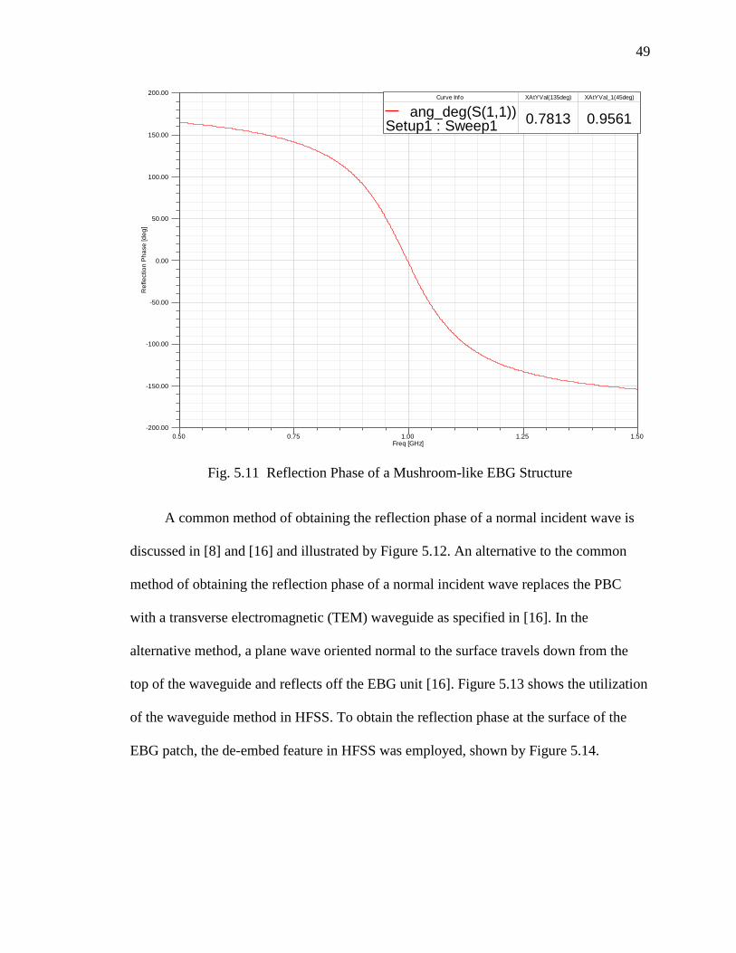
5.2.2 Reflection phase method
Another method to obtain the frequency of the surface wave band gap is to acquire
the reflection phase of a normal incident wave on a unit of the EBG structure, shown in
Figure 5.11. For a mushroom-like EBG structure, the band gap is found between 135
degrees to 45 degrees [14], [15].
0.00 20.00 40.00 60.00 80.00 100.00 120.00 140.00 160.00 180.00px [deg]
2.50E+008
5.00E+008
7.50E+008
1.00E+009
1.25E+009
1.50E+009
1.75E+009
2.00E+009
2.25E+009
Fre
qu
en
cy
m2
m1
Name X Y
m1 30.0000 759083923.0364
m2 36.1897 1176775121.9227
Page 64
49
Fig. 5.11 Reflection Phase of a Mushroom-like EBG Structure
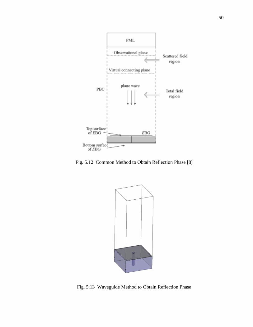
A common method of obtaining the reflection phase of a normal incident wave is
discussed in [8] and [16] and illustrated by Figure 5.12. An alternative to the common
method of obtaining the reflection phase of a normal incident wave replaces the PBC
with a transverse electromagnetic (TEM) waveguide as specified in [16]. In the
alternative method, a plane wave oriented normal to the surface travels down from the
top of the waveguide and reflects off the EBG unit [16]. Figure 5.13 shows the utilization
of the waveguide method in HFSS. To obtain the reflection phase at the surface of the
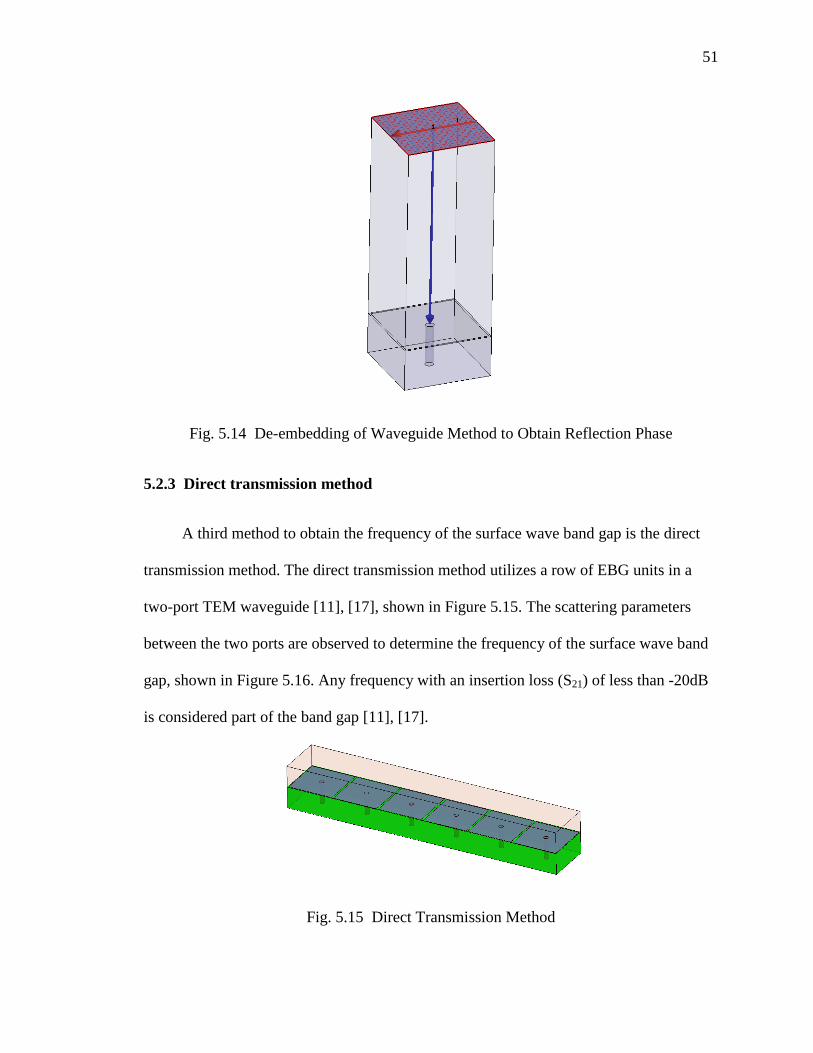
EBG patch, the de-embed feature in HFSS was employed, shown by Figure 5.14.
0.50 0.75 1.00 1.25 1.50Freq [GHz]
-200.00
-150.00
-100.00
-50.00
0.00
50.00
100.00
150.00
200.00
Re
fle
ctio
n P
ha
se
[d
eg
]
Curve Info XAtYVal(135deg) XAtYVal_1(45deg)
ang_deg(S(1,1))Setup1 : Sweep1
0.7813 0.9561
Page 65
50
Fig. 5.12 Common Method to Obtain Reflection Phase [8]
Fig. 5.13 Waveguide Method to Obtain Reflection Phase
Page 66
51
Fig. 5.14 De-embedding of Waveguide Method to Obtain Reflection Phase
5.2.3 Direct transmission method
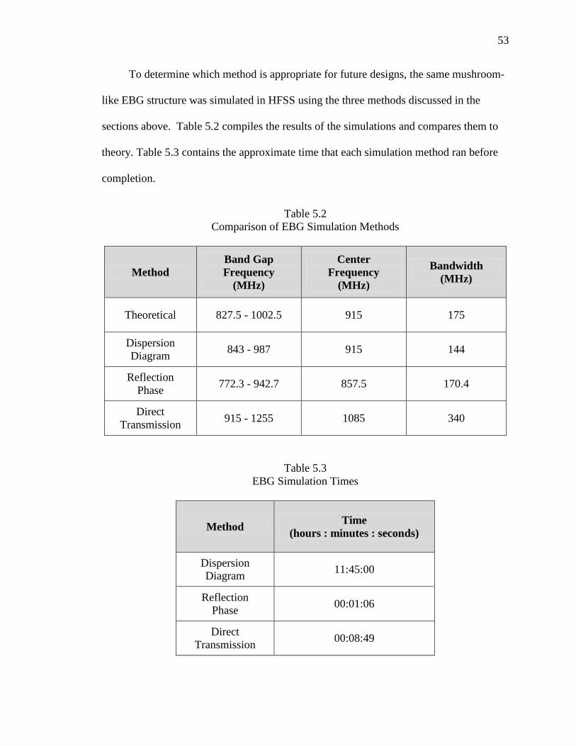
A third method to obtain the frequency of the surface wave band gap is the direct
transmission method. The direct transmission method utilizes a row of EBG units in a
two-port TEM waveguide [11], [17], shown in Figure 5.15. The scattering parameters
between the two ports are observed to determine the frequency of the surface wave band
gap, shown in Figure 5.16. Any frequency with an insertion loss (S21) of less than -20dB
is considered part of the band gap [11], [17].
Fig. 5.15 Direct Transmission Method
Page 67
52
Fig. 5.16 Scattering Parameters From Direct Transmission Method
5.2.4 Comparison of simulation methods
The dispersion diagram method consistently provides an accurate set of data.
Therefore, the dispersion diagram method is commonly used as a form of verification of
other methods, as shown in [11] and [17]. Though the reflection phase method provides
accurate results for mushroom-like EBG structures, it cannot be universally used to find
the band gap for all EBG structures [15]; this is the reason the reflection phase method is
not regarded as the most consistent. Due to coupling with the top of the waveguide, the
direct transmission method generates less reliable data than both the dispersion diagram
and reflection phase methods [11].
0.63 0.75 0.88 1.00 1.13 1.25 1.38 1.50Freq [GHz]
-60.00
-50.00
-40.00
-30.00
-20.00
-10.00
0.00
Y1
m2m1
Name X Y
m1 0.9150 -19.9848
m2 1.2550 -20.0253
Curve Info
dB(S(1,1))Setup1 : Sweep1
dB(S(2,1))Setup1 : Sweep1
Page 68
53
To determine which method is appropriate for future designs, the same mushroom-
like EBG structure was simulated in HFSS using the three methods discussed in the
sections above. Table 5.2 compiles the results of the simulations and compares them to
theory. Table 5.3 contains the approximate time that each simulation method ran before
completion.
Table 5.2
Comparison of EBG Simulation Methods
Method
Band Gap
Frequency
(MHz)
Center
Frequency
(MHz)
Bandwidth
(MHz)
Theoretical 827.5 - 1002.5 915 175
Dispersion
Diagram 843 - 987 915 144
Reflection
Phase 772.3 - 942.7 857.5 170.4
Direct
Transmission 915 - 1255 1085 340
Table 5.3
EBG Simulation Times
Method Time
(hours : minutes : seconds)
Dispersion
Diagram 11:45:00
Reflection
Phase 00:01:06
Direct
Transmission 00:08:49
Page 69
54
As expected, the dispersion diagram method obtained results that corresponded best
with the theoretical center frequency. However, the amount of time that was required for
simulation of the dispersion diagram was extremely long, especially compared to its
counterparts. Meanwhile, the reflection phase method produced results that were
comparable to the theoretical center frequency in a fraction of the time. The reflection
phase method also produced results with a bandwidth closest to theory. The direct
transmission method appears to have no redeeming qualities, as it produced results that
were furthest from theory and took longer than the reflection phase method.
In summation, to quickly characterize the mushroom-like EBG structure, the
reflection phase method will be employed. Since the results of the dispersion diagram
method were the closest to theoretical center frequency and are commonly used for
verification, the final design will be verified with the dispersion diagram method.
5.3 Parametric Study of Mushroom-like EBG Structures
The reflection phase method was used to observe the effects of varying the width
and gap size of an EBG unit and the radius of a via. The radius of the via was varied from
0.5mm to 1.5mm in increments of 0.1mm. Figure 5.17 graphs the results of the
simulation with varying radii. As expected, there was little change as the radius was
varied, which is why the radius size is not included in theoretical equations. Therefore, a
radius of 1mm will be used in future designs.
Page 70
55
Fig. 5.17 Reflection Phase Results From Varying Radius of a Via
The width of the EBG unit was varied from 20mm to 22mm in increments of
0.2mm. Figure 5.18 is a graph of the results from varying width. The results from varying
width agree with theory; a greater width equates to a lower center frequency, as can be
determined by Equation 5.5.
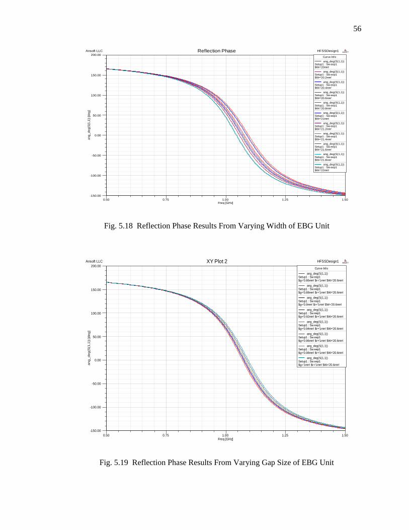
The EBG gap size was varied from 0.86mm to 1mm in increments of 0.02mm.
Figure 5.19 is a graph of the results from varying the gap size. The results from varying
the gap size agree with theory; a greater gap equates to a higher center frequency, as can
be derived from Equation 5.5.
0.50 0.75 1.00 1.25 1.50Freq [GHz]
-150.00
-100.00
-50.00
0.00
50.00
100.00
150.00
200.00
an
g_
de
g(S
(1,1
)) [d
eg
]
Ansoft LLC HFSSDesign1XY Plot 1 ANSOFT
Curve Info
ang_deg(S(1,1))Setup1 : Sw eep1$g='0.92mm' $r='0.5mm' $W='20.6mm'
ang_deg(S(1,1))Setup1 : Sw eep1$g='0.92mm' $r='0.6mm' $W='20.6mm'
ang_deg(S(1,1))Setup1 : Sw eep1$g='0.92mm' $r='0.7mm' $W='20.6mm'
ang_deg(S(1,1))Setup1 : Sw eep1$g='0.92mm' $r='0.8mm' $W='20.6mm'
ang_deg(S(1,1))Setup1 : Sw eep1$g='0.92mm' $r='0.9mm' $W='20.6mm'
ang_deg(S(1,1))Setup1 : Sw eep1$g='0.92mm' $r='1mm' $W='20.6mm'
ang_deg(S(1,1))Setup1 : Sw eep1$g='0.92mm' $r='1.1mm' $W='20.6mm'
ang_deg(S(1,1))Setup1 : Sw eep1$g='0.92mm' $r='1.2mm' $W='20.6mm'
ang_deg(S(1,1))Setup1 : Sw eep1$g='0.92mm' $r='1.3mm' $W='20.6mm'
ang_deg(S(1,1))Setup1 : Sw eep1$g='0.92mm' $r='1.4mm' $W='20.6mm'
ang_deg(S(1,1))Setup1 : Sw eep1$g='0.92mm' $r='1.5mm' $W='20.6mm'
Page 71
56
Fig. 5.18 Reflection Phase Results From Varying Width of EBG Unit
Fig. 5.19 Reflection Phase Results From Varying Gap Size of EBG Unit
0.50 0.75 1.00 1.25 1.50Freq [GHz]
-150.00
-100.00
-50.00
0.00
50.00
100.00
150.00
200.00
an
g_
de
g(S
(1,1
)) [d
eg
]
Ansoft LLC HFSSDesign1Reflection Phase ANSOFT
Curve Info
ang_deg(S(1,1))Setup1 : Sw eep1$W='20mm'
ang_deg(S(1,1))Setup1 : Sw eep1$W='20.2mm'
ang_deg(S(1,1))Setup1 : Sw eep1$W='20.4mm'
ang_deg(S(1,1))Setup1 : Sw eep1$W='20.6mm'
ang_deg(S(1,1))Setup1 : Sw eep1$W='20.8mm'
ang_deg(S(1,1))Setup1 : Sw eep1$W='21mm'
ang_deg(S(1,1))Setup1 : Sw eep1$W='21.2mm'
ang_deg(S(1,1))Setup1 : Sw eep1$W='21.4mm'
ang_deg(S(1,1))Setup1 : Sw eep1$W='21.6mm'
ang_deg(S(1,1))Setup1 : Sw eep1$W='21.8mm'
ang_deg(S(1,1))Setup1 : Sw eep1$W='22mm'
0.50 0.75 1.00 1.25 1.50Freq [GHz]
-150.00
-100.00
-50.00
0.00
50.00
100.00
150.00
200.00
an
g_
de
g(S
(1,1
)) [d
eg
]
Ansoft LLC HFSSDesign1XY Plot 2 ANSOFT
Curve Info
ang_deg(S(1,1))Setup1 : Sw eep1$g='0.86mm' $r='1mm' $W='20.6mm'
ang_deg(S(1,1))Setup1 : Sw eep1$g='0.88mm' $r='1mm' $W='20.6mm'
ang_deg(S(1,1))Setup1 : Sw eep1$g='0.9mm' $r='1mm' $W='20.6mm'
ang_deg(S(1,1))Setup1 : Sw eep1$g='0.92mm' $r='1mm' $W='20.6mm'
ang_deg(S(1,1))Setup1 : Sw eep1$g='0.94mm' $r='1mm' $W='20.6mm'
ang_deg(S(1,1))Setup1 : Sw eep1$g='0.96mm' $r='1mm' $W='20.6mm'
ang_deg(S(1,1))Setup1 : Sw eep1$g='0.98mm' $r='1mm' $W='20.6mm'
ang_deg(S(1,1))Setup1 : Sw eep1$g='1mm' $r='1mm' $W='20.6mm'
Page 72
57
6. ANTENNA DESIGNS WITH EBG STRUCTURES
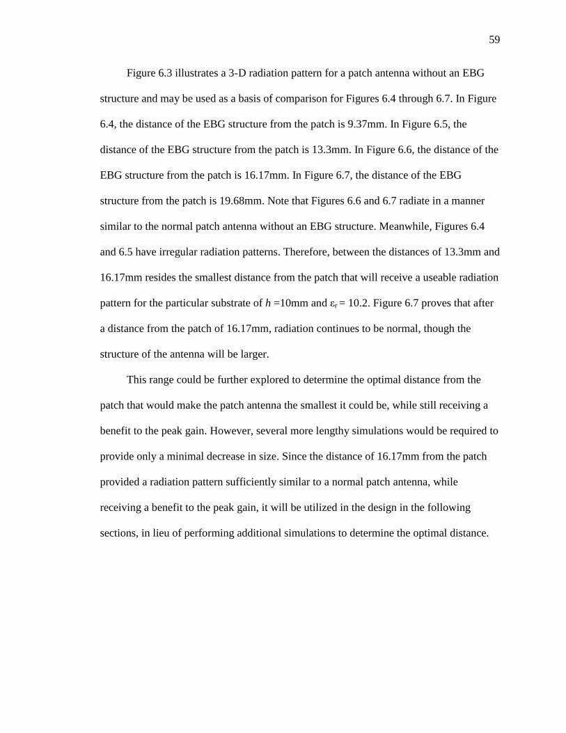
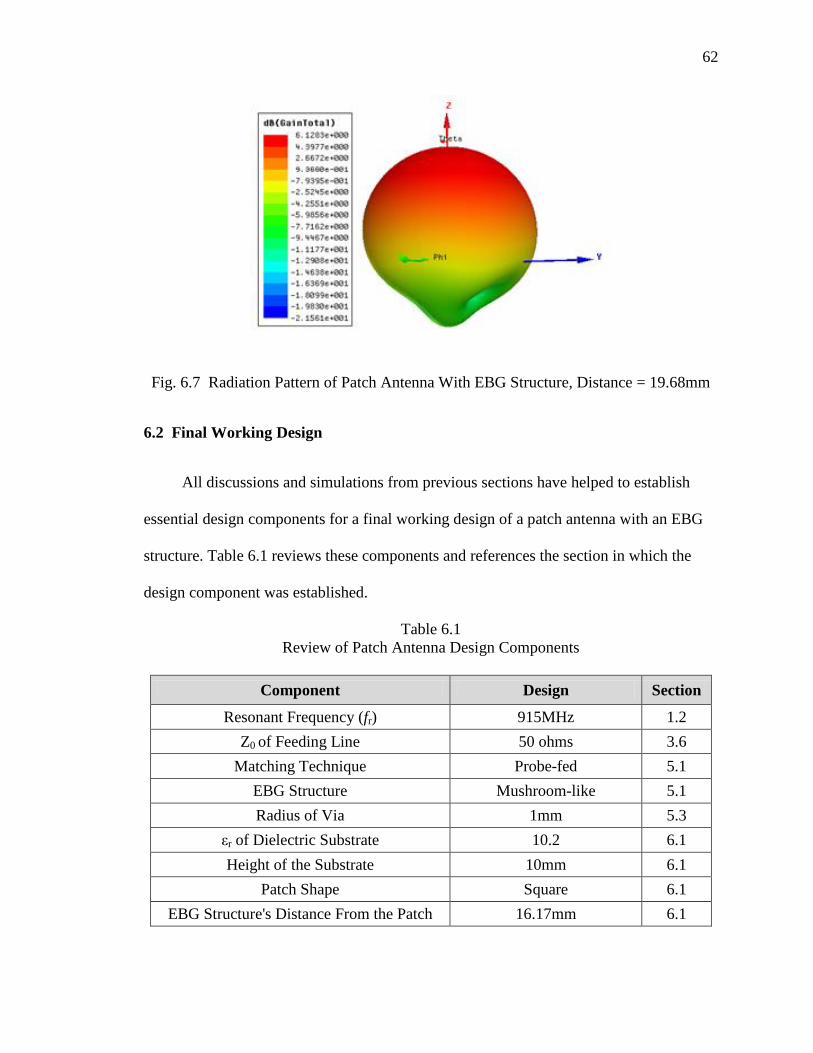
6.1 EBG Distance From Patch
As stated in Section 5.1, a mushroom-like EBG structure will be placed around a
UHF RFID probe-fed patch antenna. For comparison, many probe-fed antenna
simulations were performed with and without EBG structures. Select results of
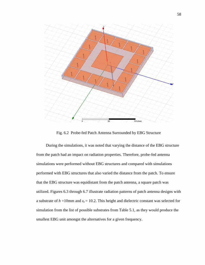
importance will be discussed in this section. Figures 6.1 and 6.2 show simulations of
probe-fed patch antennas with and without EBG structures.
Fig. 6.1 Probe-fed Patch Antenna Without EBG Structure
Page 73
58
Fig. 6.2 Probe-fed Patch Antenna Surrounded by EBG Structure
During the simulations, it was noted that varying the distance of the EBG structure
from the patch had an impact on radiation properties. Therefore, probe-fed antenna
simulations were performed without EBG structures and compared with simulations
performed with EBG structures that also varied the distance from the patch. To ensure
that the EBG structure was equidistant from the patch antenna, a square patch was
utilized. Figures 6.3 through 6.7 illustrate radiation patterns of patch antenna designs with
a substrate of h =10mm and εr = 10.2. This height and dielectric constant was selected for
simulation from the list of possible substrates from Table 5.1, as they would produce the
smallest EBG unit amongst the alternatives for a given frequency.
Page 74
59
Figure 6.3 illustrates a 3-D radiation pattern for a patch antenna without an EBG
structure and may be used as a basis of comparison for Figures 6.4 through 6.7. In Figure
6.4, the distance of the EBG structure from the patch is 9.37mm. In Figure 6.5, the
distance of the EBG structure from the patch is 13.3mm. In Figure 6.6, the distance of the
EBG structure from the patch is 16.17mm. In Figure 6.7, the distance of the EBG
structure from the patch is 19.68mm. Note that Figures 6.6 and 6.7 radiate in a manner
similar to the normal patch antenna without an EBG structure. Meanwhile, Figures 6.4
and 6.5 have irregular radiation patterns. Therefore, between the distances of 13.3mm and
16.17mm resides the smallest distance from the patch that will receive a useable radiation
pattern for the particular substrate of h =10mm and εr = 10.2. Figure 6.7 proves that after
a distance from the patch of 16.17mm, radiation continues to be normal, though the
structure of the antenna will be larger.
This range could be further explored to determine the optimal distance from the
patch that would make the patch antenna the smallest it could be, while still receiving a
benefit to the peak gain. However, several more lengthy simulations would be required to
provide only a minimal decrease in size. Since the distance of 16.17mm from the patch
provided a radiation pattern sufficiently similar to a normal patch antenna, while
receiving a benefit to the peak gain, it will be utilized in the design in the following
sections, in lieu of performing additional simulations to determine the optimal distance.
Page 75
60
Fig. 6.3 3-D Radiation Pattern of Patch Antenna Without EBG Structure
Fig. 6.4 Radiation Pattern of Patch Antenna With EBG Structure, Distance = 9.37mm
Page 76
61
Fig. 6.5 Radiation Pattern of Patch Antenna With EBG Structure, Distance = 13.3mm
Fig. 6.6 Radiation Pattern of Patch Antenna With EBG Structure, Distance = 16.17mm
Page 77
62
Fig. 6.7 Radiation Pattern of Patch Antenna With EBG Structure, Distance = 19.68mm
6.2 Final Working Design
All discussions and simulations from previous sections have helped to establish
essential design components for a final working design of a patch antenna with an EBG
structure. Table 6.1 reviews these components and references the section in which the
design component was established.
Table 6.1
Review of Patch Antenna Design Components
Component Design Section
Resonant Frequency (fr) 915MHz 1.2
Z0 of Feeding Line 50 ohms 3.6
Matching Technique Probe-fed 5.1
EBG Structure Mushroom-like 5.1
Radius of Via 1mm 5.3
εr of Dielectric Substrate 10.2 6.1
Height of the Substrate 10mm 6.1
Patch Shape Square 6.1
EBG Structure's Distance From the Patch 16.17mm 6.1
Page 78
63
Utilizing the components in Table 6.1, a patch antenna with and without EBG
structures was designed that had return loss optimized to the resonant frequency by
parametric studies. To obtain an intial starting point for optimizing the size of the patch
and location of the feed, the transmission line model with mutual effects included was
employed. The parameters of the final working design are listed in Table 6.2.
Table 6.2
Final Working Design Parameters
Parameter Patch Antenna
Without EBG
Patch Antenna
With EBG
Substrate
Height 10mm 10mm
Dielectric Constant 10.2 10.2
Length 130mm 130mm
Width 130mm 130mm
Patch
Length 46.65mm 46.5mm
Width 46.65mm 46.5mm
Feed Location
y0 14.925mm 16.4mm
EBG Structure
Width 23.6mm
Gap 2.01mm
Radius of Vias 1mm
Distance From Patch 16.17mm
Number of Units 16
Number of Rows 1
Page 79
64
6.2.1 Analysis
The two designs outlined in Table 6.2 were compared in simulations to determine if
placing an EBG structure around a patch antenna improves figures-of-merit such as peak
gain. Figures 6.8 and 6.9 graph the gain of the patch antenna with and without EBG
structures. The graphs clearly show an improvement in peak gain when the EBG structure
was employed. This gain improvement is one of the benefits of suppressing surface
waves, as discussed in Section 5.1.
Fig. 6.8 Gain of Patch Antenna Without EBG Structure
-200.00 -150.00 -100.00 -50.00 0.00 50.00 100.00 150.00 200.00Theta [deg]
-20.00
-15.00
-10.00
-5.00
0.00
5.00
10.00
Y1
Ansoft LLC Patch 200x200ff_2D_GainTotal ANSOFT
Curve Info max
dB(GainTotal)Setup1 : LastAdaptiveFreq='0.915GHz' Phi='0deg'
5.6879
dB(GainTotal)_1Setup1 : LastAdaptiveFreq='0.915GHz' Phi='90deg'
5.6879
Page 80
65
Fig. 6.9 Gain of Patch Antenna With EBG Structure
The radiation patterns will be further analzyed with Figures 6.10 and 6.11. Figure
6.10 shows the radiation pattern of the patch antenna without an EBG structure. Figure
6.11 shows the radiation pattern of the patch antenna with an EBG structure. 3-D
radiation patterns of the patch antenna with and without EBG structures are found in
Figures 6.3 and 6.6. After examining the radiation patterns, it is clear that the back lobe
is reduced when the EBG structure is implemented, increasing directivity. This reduction
in the back lobe is one of the benefits of suppressing surface waves, as discussed in
Section 5.1.
-200.00 -150.00 -100.00 -50.00 0.00 50.00 100.00 150.00 200.00Theta [deg]
-12.50
-10.00
-7.50
-5.00
-2.50
0.00
2.50
5.00
7.50
dB
(Ga
inT
ota
l)
Patch_Antenna_ADKv1XY Plot 2 ANSOFT
Curve Info max
dB(GainTotal)Setup1 : LastAdaptiveFreq='0.915GHz' Phi='0deg'
6.1636
dB(GainTotal)Setup1 : LastAdaptiveFreq='0.915GHz' Phi='90deg'
6.1648
Page 81
66
Fig. 6.10 Radiation Pattern of Patch Without EBG Structure
Fig. 6.11 Radiation Pattern of Patch With EBG Structure
-14.00
-8.00
-2.00
4.00
90
60
30
0
-30
-60
-90
-120
-150
-180
150
120
Patch 200x200Radiation Pattern ANSOFT
Curve Info max
dB(GainTotal)Setup1 : LastAdaptiveFreq='0.915GHz' Phi='0deg'
5.6879
dB(GainTotal)Setup1 : LastAdaptiveFreq='0.915GHz' Phi='90deg'
5.6879
-8.50
-4.50
-0.50
3.50
90
60
30
0
-30
-60
-90
-120
-150
-180
150
120
Patch_Antenna_ADKv1Radiation Pattern ANSOFT
Curve Info max
dB(GainTotal)Setup1 : LastAdaptiveFreq='0.915GHz' Phi='0deg'
6.1636
dB(GainTotal)Setup1 : LastAdaptiveFreq='0.915GHz' Phi='90deg'
6.1648
Page 82
67
The bandwidth and return loss of the antennas will be analzyed with Figures 6.12
and 6.13. The acceptable bandwidth is assumed to be at a voltage standing wave ratio
(VSWR) of 2:1 which equates to a return loss of -9.54dB. Figure 6.12 shows the
bandwidth and return loss of the patch antenna without an EBG structure. Figure 6.13
shows the bandwidth and return loss of the patch antenna with an EBG structure. After
examining Figures 6.12 and 6.13, it is clear that there is a decrease in bandwidth when
the EBG structure is implemented. This decrease in bandwidth contradicts the statement
from [8] in Section 5.1. However, this does not prove that the bandwidth cannot be
increased by the implementation of EBG structures, as many other simulations with EBG
structures increased the bandwidth, such as the simulations performed in Section 6.1. The
figures also show that the return loss at the resonant frequency is relatively the same for
both.
For review, Table 6.3 compares the overall results of the simulations. The EBG
verification results are shown as dispersion diagram figures in Section 5.2.1 and listed in
Table 6.4.
Table 6.3
Overall Results of Final Working Design
Resonant
Frequency
(MHz)
Return
Loss
(dB)
Bandwidth
(MHz)
Peak Gain
(dB)
Front-to-
back (dB)
Patch
Without
EBG
915 -48.17 28.17 5.6879 9.5497
Patch
With EBG 915 -48.39 17.28 6.1648 11.0656
Page 83
68
Fig. 6.12 Return Loss of Patch Antenna Without EBG Structure
Fig. 6.13 Return Loss of Patch Antenna With EBG Structure
890.00 900.00 910.00 920.00 930.00 940.00Freq [MHz]
-50.00
-40.00
-30.00
-20.00
-10.00
0.00
dB
(St(
1,1
))
Ansoft LLC Patch 200x200Return Loss ANSOFT
Curve Info XAtYMin min XWidthAtYVal(-9.54)
dB(St(1,1))Setup1 : Sweep1
915.0000 -48.1665 28.1706
890.00 900.00 910.00 920.00 930.00 940.00Freq [MHz]
-50.00
-40.00
-30.00
-20.00
-10.00
0.00
dB
(St(
1,1
))
Patch_Antenna_ADKv1Return Loss ANSOFT
Curve Info XAtYMin min XWidthAtYVal(-9.54)
dB(St(1,1))Setup1 : Sweep1
915.0000 -48.3925 17.2799
Page 84
69
Table 6.4
Dispersion Diagram Results for EBG Verification
Method
Band Gap
Frequency
(MHz)
Center
Frequency
(MHz)
Bandwidth
(MHz)
Theoretical 827.5 - 1002.5 915 175
Dispersion
Diagram 771.3 - 976.1 873.7 204.8
The results from the dispersion diagram and theory verify that the resonant frequency and
bandwidth of the final working design are included in the frequency band gap.
The size of the ground plane on the antenna design with and without EBG
structures was increased to observe how the antennas would perform on metallic surfaces
of varying size. The ground plane was increased from 130mm by 130mm to 500mm by
500mm, with simulations at 200mm by 200mm and 300mm by 300mm. The results from
simulating an increase in the ground plane are placed in Tables 6.5 and 6.6. The radiation
patterns of the antenna designs with EBG structures are shown in Figures 6.14, 6.16, and
6.18. The radiation patterns of the antenna designs without EBG structures are shown in
Figures 6.15, 6.17, and 6.19.
Page 85
70
Table 6.5
Increasing Ground Plane of Patch Antenna With EBG Structure
Ground
Plane
(mm x mm)
Resonant
Frequency
(MHz)
Return
Loss
(MHz)
Bandwidth
(MHz)
Peak
Gain
(dB)
130 x 130 915 -48.39 17.28 6.1648
200 x 200 919 -18.33 14.46 6.1917
300 x 300 918 -14.79 12.14 5.6481
500 x 500 918 -15.69 12.84 5.8219
Table 6.6
Increasing Ground Plane of Patch Antenna Without EBG Structure
Ground
Plane
(mm x mm)
Resonant
Frequency
(MHz)
Return
Loss
(MHz)
Bandwidth
(MHz)
Peak
Gain
(dB)
130 x 130 915 -48.17 28.17 5.6879
200 x 200 916 -11.6629 13.4085 5.7403
300 x 300 914 -9.8917 5.6896 5.2065
500 x 500 914 -10.6202 9.8435 5.4000
Page 86
71
Fig. 6.14 EBG Patch Antenna With Ground Plane 200mm by 200mm
Fig. 6.15 Normal Patch Antenna With Ground Plane 200mm by 200mm
-14.00
-8.00
-2.00
4.00
90
60
30
0
-30
-60
-90
-120
-150
-180
150
120
Curve Info
dB(GainTotal)Setup1 : LastAdaptiveFreq='0.915GHz' Phi='0deg'
dB(GainTotal)Setup1 : LastAdaptiveFreq='0.915GHz' Phi='90deg'
-14.00
-8.00
-2.00
4.00
90
60
30
0
-30
-60
-90
-120
-150
-180
150
120
Curve Info
dB(GainTotal)Setup1 : LastAdaptiveFreq='0.915GHz' Phi='0deg'
dB(GainTotal)Setup1 : LastAdaptiveFreq='0.915GHz' Phi='90deg'
Page 87
72
Fig. 6.16 EBG Patch Antenna With Ground Plane 300mm by 300mm
Fig. 6.17 Normal Patch Antenna With Ground Plane 300mm by 300mm
-22.00
-14.00
-6.00
2.00
90
60
30
0
-30
-60
-90
-120
-150
-180
150
120
Curve Info
dB(GainTotal)Setup1 : LastAdaptiveFreq='0.915GHz' Phi='0deg'
dB(GainTotal)Setup1 : LastAdaptiveFreq='0.915GHz' Phi='90deg'
-14.00
-8.00
-2.00
4.00
90
60
30
0
-30
-60
-90
-120
-150
-180
150
120
Curve Info
dB(GainTotal)Setup1 : LastAdaptiveFreq='0.915GHz' Gnd='300mm' Phi='0deg'
dB(GainTotal)Setup1 : LastAdaptiveFreq='0.915GHz' Gnd='300mm' Phi='90deg'
Page 88
73
Fig. 6.18 EBG Patch Antenna With Ground Plane 500mm by 500mm
Fig. 6.19 Normal Patch Antenna With Ground Plane 500mm by 500mm
-18.00
-11.00
-4.00
3.00
90
60
30
0
-30
-60
-90
-120
-150
-180
150
120
Curve Info
dB(GainTotal)Setup1 : LastAdaptiveFreq='0.915GHz' Phi='0deg'
dB(GainTotal)Setup1 : LastAdaptiveFreq='0.915GHz' Phi='90deg'
-14.00
-8.00
-2.00
4.00
90
60
30
0
-30
-60
-90
-120
-150
-180
150
120
Curve Info
dB(GainTotal)Setup1 : LastAdaptiveFreq='0.915GHz' Gnd='500mm' Phi='0deg'
dB(GainTotal)Setup1 : LastAdaptiveFreq='0.915GHz' Gnd='500mm' Phi='90deg'
Page 89
74
Table 6.5 and the radiation patterns show that the final working design is useable
on metallic surfaces of varying size, as the bandwidths remain in the UHF RFID band
and the radiation patterns are not irregular. When increasing the ground plane from
130mm by 130mm, the increase in peak gain found by utilizing the EBG structure in the
design remained consistent. As expected, because the return losses of the designs were
optimized with the ground plane of 130mm by 130mm, the return loss results for both
designs increased as the ground plane varied from 130mm by 130mm. This increase in
return loss did not affect the design with an EBG structure as much as the design without
an EBG structure. More importantly, note the great decrease in bandwidth of the design
without an EBG structure. At 130mm by 130mm, the design without the EBG structure
had a much larger bandwidth than the design with the EBG structure. However, when the
ground plane was increased from 130mm by 130mm, the bandwidth results of the design
with an EBG structure were larger than the bandwidth results of the design without an
EBG structure.
As discussed, when the ground plane was increased the design with the EBG
structure outperformed the design without the EBG structure in every figure-of-merit
taken into account. Therefore, utilization of the EBG structure increased the ability of the
patch antenna to be mounted on multiple metallic surfaces.
6.3 Similar Research
Currently, there are several institutions conducting research on implementing EBG
structures with UHF RFID tag antennas that are mountable on metal. In [2], a patch
antenna is utilized with periodic holes placed in the ground plane to create a surface wave
Page 90
75
band gap. The antenna was manufactured and tested for read range. The tests included
mounting the antenna to metallic plates of varying size. Similar to the results from the
final working design in section 6.2.1, there was an improvement in read range, or gain, in
all the tested cases. In [10], a two-layer mushroom-like EBG structure is utilized with a
folded dipole antenna. The design used a ferrite material to minimize the structure's size.
The ANSYS HFSS simulation results showed an improvement in the antenna's gain and
radiation pattern. In [18], two different dipole-type antennas were placed above an EBG
surface. The antennas were manufactured and tested after being designed and analyzed
on CST Microwave Studio. During testing, the antennas were placed on a large metallic
surface and in free space. Both situations achieved good read ranges. In summation, the
results of similar research agree with the results produced by this research.
Page 91
76
7. CONCLUSIONS
A novel UHF RFID tag antenna has been designed and analyzed in ANSYS HFSS.
The antenna has a low profile, long range, and is mountable on metallic surfaces. The
microstrip patch antenna was selected because it is inherently low profile. Different
matching techniques and theoretical models for the patch antenna were investigated. The
results of investigating matching techniques led to three possible ways to match the
antenna: inset-feeding, probe-feeding, and using a quarter-wave transformer.
Investigating the transmission line model and cavity model led to the conclusion that, for
UHF RFID patch antennas, input impedance was best estimated by the transmission line
model with mutual effects included. After investigating the matching and theory of a
patch antenna, a design technique utilizing an EBG structure was explored to increase the
range, or peak gain, of the patch antenna. The analysis of the design technique utilizing
the EBG structure showed improvement in peak gain and in the ability to be mounted on
multiple metallic surfaces.
Future work should include more simulations. A set of simulations should be
performed to determine under which conditions the utilization of an EBG structure
increases bandwidth. Another set of simulations should be performed to determine the
smallest distance an EBG structure could be positioned from the patch without receiving
an irregular radiation pattern, as first discussed in Section 6.1. Other antenna design
Page 92
77
techniques that utilize EBG structures should also be explored, such as periodic holes in
the substrate or ground plane, shown in Figure 7.1. The final working design should be
manufactured and undergo testing for validation. These tests would include
measurements of scattering parameters performed with a network analyzer and of the
radiation pattern performed in an anechoic chamber.
Fig. 7.1 Periodic Holes in the Ground Plane
Page 94
78
BIBLIOGRAPHY
[1] “The basics of RFID technology.” RFID Journal. [Online]. Available:
http://www.rfidjournal.com/article/view/1337/1 [Apr. 1, 2012].
[2] L. Ukkonen et. al., “Effects of metallic plate size on the performance
of microstrip patch-type tag antennas for passive RFID,” IEEE Antennas Wireless
Propag. Lett., vol. 4, pp. 410-413, 2005. 10.1109/LAWP.2005.860212.
[3] G. Breed.. “The fundamentals of patch antenna design and performance,” High
Frequency Electronics [Online]. vol. 8, no. 3, pp. 48-52. Mar. 2009. Available:
http://highfrequencyelectronics.com/Archives/Mar09/HFE0309_Tutorial.pdf [Apr.
1, 2012].
[4] R. Garg et. al., Microstrip Antenna Design Handbook, Norwood, MA: Artech
House, 2001.
[5] D.G. Fang, “Microstrip Patch Antennas,” in Antenna Theory and Microstrip
Antennas, Boca Raton, FL: CRC/Taylor & Francis, 2010, ch. 3, pp. 85-110.
[6] C.A. Balanis, “Microstrip Antennas,” in Antenna Theory: Analysis and Design, 3rd
ed. Hoboken, NJ: John Wiley, 2005, ch. 14, pp. 811-882.
[7] D.M. Pozar, Microwave Engineering, 3rd
ed. Hoboken, NJ: Wiley, 2005.
[8] F. Yang and Y. Rahmat-Samii, Electromagnetic Band Gap Structures in Antenna
Engineering, Cambridge, UK: Cambridge UP, 2009.
[9] D.F. Sievenpiper, "High-impedance electromagnetic surfaces," Ph.D. dissertation,
Dept. Elect. Eng., Univ. California, Los Angeles, 1999.
http://optoelectronics.eecs.berkeley.edu/ThesisDan.pdf.
[10] B. Gao and M.M.F. Yuen, “Passive UHF RFID with ferrite electromagnetic band
gap (EBG) material for metal objects tracking,” in Electronic Components and
Technology Conf., Lake Beuna Vista, FL, May 27-30, 2008, pp. 1990-1994.
10.1109/ECTC.2008.4550256.
Page 95
79
[11] L. Liang et. al., “A novel broadband EBG using multi-period mushroom-like
structure,” in 2008 Int. Conf. Microwave and Millimeter Wave Technology, April 21-
24, vol. 4, pp. 1609-1612. 10.1109/ICMMT.2008.4540770.
[12] “HFSS Tutorial 3: Dispersion Diagram II: Sievenpiper Mushroom.” Internet:
http://www.emtalk.com/tut_3.htm, Apr. 19, 2011 [Apr. 1, 2012].
[13] “HFSS Tutorial 2: Dispersion Diagram I: Parallel Plate.” Internet:
http://www.emtalk.com/tut_2.htm, Apr. 19, 2011 [Mar. 31, 2012].
[14] F. Yang and Y. Rahmat-Samii, "Reflection phase characterization of an
electromagnetic band-gap (EBG) surface," in 2002 IEEE Antennas and Propagation
Society Int. Symp., vol. 3, pp. 744-747. 10.1109/APS.2002.1018317.
[15] F. Yang and Y. Rahmat-Samii, "Reflection phase characterizations of the EBG
ground plane for low profile wire antenna applications," IEEE Trans. Antennas
Propag., vol. 51, pp. 2691-2703, Oct. 2003. 10.1109/TAP.2003.817559.
[16] S. Mahdi Moghadasi, "Waveguide model for reflection phase characterization of
periodic EBG surfaces," in Asia Pacific Microwave Conf. 2007, December 11-14,
pp. 1-4. 10.1109/APMC.2007.4555125.
[17] W. Zhang et. al., "A novel broadband EBG using multi-via cascaded mushroom-like
structure," in Asia Pacific Microwave Conf. 2009, December 7-10, pp.484-487.
10.1109/APMC.2009.5384196.
[18] D. Sim et. al., "Design of novel dipole-type tag antennas using electromagnetic
bandgap (EBG) surface for passive RFID applications," in 2007 IEEE Antennas and
Propagation Society Int. Symp., Honolulu, HI, June 9-15, pp. 1333-1336.
10.1109/APS.2007.4395749.
Page 97
80
A. OBTAINING WIDTH AND LENGTH OF A SQUARE PATCH
// Written by Nathan Reynolds
// sPatch gives the length and width of a square patch that resonates at 915 MHz
// Input er is the dielectric constant of the substrate
// Input h is the height of the substrate in m
// Output x is the length and width of the square patch in m
function [x , fval , exitflag , output] = sPatch(er, h)
function y = patch (L)
f1 = 10/61*((er+1+(er-1)/(1+12*h/L)^(1/2))/2)^(-1/2);
f2 = 0.824*h*(((er+1+(er1)/(1+12*h/L)^(1/2))/2)+0.3)*(L/h+0.264)/
((((er+1+(er-1)/(1+12*h/L)^(1/2))/2)-0.258)*(L/h+0.8));
f3 = L;
y = abs(f1 - f2 - f3);
endfunction
x0 = 10/61/sqrt(er); // start algorithm with length being half-wavelength
opt = optimset ( "TolX" , 1.e-9 );
[x , fval , exitflag , output] = fminsearch ( patch , x0, opt );
endfunction
Page 98
81
B. OBTAINING THE WIDTH AND GAP OF AN EBG STRUCTURE
// Written by Nathan Reynolds
// EBG gives the width and gap of a mushroom-like EBG
// Resonant frequency is assumed to be 915 MHz
// Input er is the dielectric constant of the substrate
// Input h is the height of the substrate in m
// Input a is the periodic length of the EBG structure in m
// Output g is the length of the gap in m
// Output W is the length of the width in m
function [g , W, fval , exitflag , output] = EBG(er, h, a)
function y = cost(x)
f1 = (a-x)*acosh(a/x);
f2 = (10/61)^2/(%pi*h*(1+er));
y = abs(f1 - f2);
endfunction
x0 = .001; // start algorithm with gap size of 1 mm
opt = optimset ( "TolX" , 1.e-9 );
[g , fval , exitflag , output] = fminsearch ( cost , x0, opt );
W = a - g;
endfunction