LOW COST FREQUENCY SHIFT KEYING ACOUSTIC MODEM FOR UNDERWATER WIRELESS SENSOR NETWORKS Abayomi Dairo Nikola Jovic Dr. Paul Cotae [email protected][email protected][email protected]Electrical and Computer Engineering Department School of Engineering and Applied Sciences University of the District of Columbia 4200 Connecticut Ave., N.W., Washington, DC 20008 Abstract: We focus on the underwater sensor nodes that have applications in oceanographic data collection, pollution monitoring, offshore exploration, disaster prevention, assisted navigation and tactical surveillance applications. The cost of such network of sensors deployed to perform some collaborative monitoring tasks over a given area is very expensive. Significant cost of each sensor can be reduced by designing a low cost acoustic modem with the same capabilities as an expensive one. In this project, we implemented two modems communicating with each other in free air within human hearing frequency ranges (20Hz – 20kHz) using off-the-shelf components and Frequency Shift Keying (FSK) modulation. We present in detail our solution and the proof of the experimental results. Key words: wireless sensor networks, underwater acoustic communication, FSK modulation. 36 Proceedings of the Spring 2013 Mid-Atlantic Section Conference of the American Society of Engineering Education
Transcript
LOW COST FREQUENCY SHIFT KEYING ACOUSTIC MODEM FOR UNDERWATER WIRELESS SENSOR NETWORKS
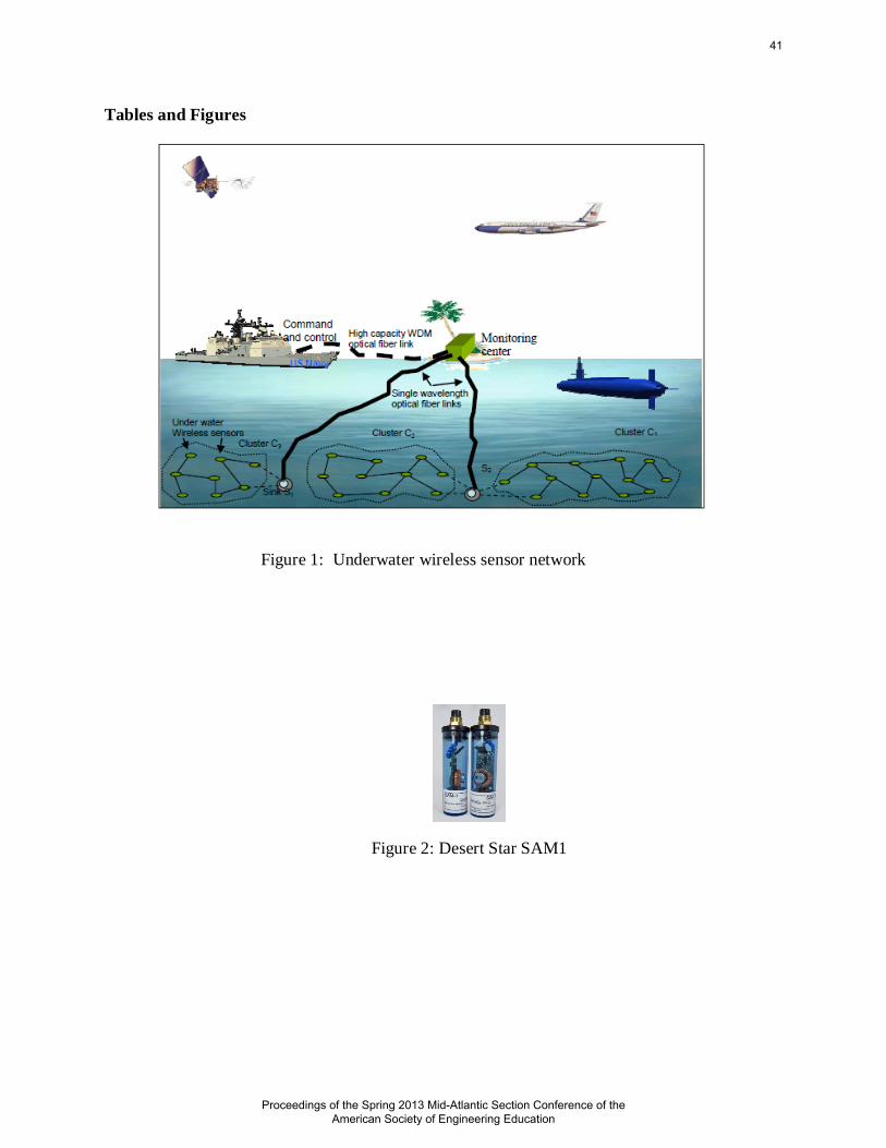
Acoustic underwater communications are governed by three factors: limited bandwidth, time-varying multipath propagation, and low speed of sound in water [1] and [2]. In underwater environments, radio waves do not propagate well due to above environmental conditions so acoustic channels are employed. The propagation speed of acoustic signals in water is about 1.5x10³ m/s, five orders of magnitude lower than the radio propagation speed 3x10⁸ m/s. In addition, the bandwidth and the capacity of underwater acoustic channels are limited and depend on both transmission range and frequency. Using a densely deployed sensor networks, we can target acoustic communication distances of 100-500 m with an expected transfer data up to 20kb/s using currently available sensor technology. In the sensor system architecture presented in Fig. 1, the underwater sensor nodes (labeled as Sink S1 and S2) with wireless acoustic modems are densely distributed in a 3-D dimensional underwater space. Each underwater sensor node can monitor and detect environmental events locally. The acoustic modems are positioned in clusters on the sea floor and they communicate with the center of command and control (CC) via monitoring center (MC). The sinks (equipped with a high-bandwidth radio frequency radio frequency communication module and a low-bandwidth acoustic communication module) relay the received data to the CC center through radio links. Thus, this underwater acoustic communication network is connected with the MC through wireless modems. According to the underwater acoustic communication research supported by a grant from the Department of Defense (DOD, mentioned the Acknowledgments section) the cost of deployed acoustic modems in a cluster underwater is very expensive. Each acoustic modem cost more than $3,000.00. The purpose of our project was to use cheaper underwater modems that would be connected into a Wireless Sensor Network (WSN) having the same capabilities as the before mentioned underwater acoustic modems but their cost would be significantly lower namely around $1000. In this paper we present the design, the principle of operation, the experimental results for two acoustic modems that could be incorporated in any underwater sensor used for applications in oceanographic data collection, pollution monitoring, offshore exploration, disaster prevention, assisted navigation and tactical surveillance applications. Our task was first, to create a prototype of an acoustic modem that can communicate wireless in free air. In this sense we have designed two prototypes of acoustic modems that can communicate by using sound waves that are within human hearing frequency ranges (20Hz – 20kHz). Price of each of these modems was around $50. Second, we want to visualize the data that was sent and received between the two modems together with the signal delays and to present the details of our design. The rest of the paper is organized as following: Section II gives a brief example of currently available underwater acoustic modems. Section III explains design and goes in depth into principle of operation of our acoustic modem. In Section IV the hardware design of each of major components of our acoustic modem are given. In this section are also show calculations of values of all electronic components that are part of these acoustic modems. Section V concludes our paper. II. Example of currently used underwater acoustic modem
Under previously mentioned research grant we had work with Desert Star SAM1 Acoustic Modem [3] which is presented in Fig.2. It’s cost and performance capabilities are as following:
37
Proceedings of the Spring 2013 Mid-Atlantic Section Conference of the American Society of Engineering Education
cost: $2614.50; working depth range: 300 meters; operating frequency: 38.2 to 42 kHz; Data rate: 4800 bauds. The starting point for our research were two publication by Benson [4] and Malysa [5].These papers describe prototypes of underwater acoustic modem. In these prototypes modulation and demodulation were implemented by using a microcontroller and a FPGA board. By contrast, in our project we used modulation and demodulation performed within electrical circuits that we have designed. III. Design and principle of operation of acoustic modem
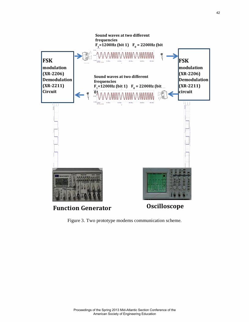
Principle of operation of our proposed project consist in a pair of acoustic modems is presented in Fig. 3 and it is as following. The acoustic modem receives digital data, “0” and “1”, from function generator. The data were then modulated using frequency shift keying (FSK) circuit. The FSK circuit creates two analog signals, at frequencies of 1.2 kHz and 2.2 kHz respectively. These signals are then demodulated in FSK demodulation circuit. Demodulated signals are then displayed on the oscilloscope. Although our modem operates in air, it is a proof-of-concept experiment in data transmission techniques that will be used to design a system capable of communicating in the underwater environment. The prototype is presented in Fig.3. In first step, the function generator creates square wave with values of 0V and 2V. These two values represent digital signals, namely 0V is logical “0” and 2V is logical “1”, respectivelly. This signal is aplied at the input of a FSK circuit part of the accoustic modem. If logical “0” is on the input analog signal on the output is Acos(2𝜋2200t). If logical “1” is on the imput then analog signal on the output is Acos(2𝜋1200t). Imput signal and output signal can be seen in Figure 5. The value of the signal on the output of the FSK modulation circuit was around 100mV. This voltage value was not strong enough to drive the speaker. So the FSK modulated signal was applied into power amplifier. In the power amplifier, signal was amplified 120 times. Signal from the output of power amplifier went into speaker. In the speaker two distinct sounds were created according to the frequency of the input signal. These two sounds propagate freely through air. On the distances up to 3m they are picked up with microphone of second acoustic modem. Signal on the input of the speaker of the first acoustic modem and the signal on the output of the microphone of the second acoustic modem are displayed in Figure 6. As mentioned before output of microphone of the second acoustic modem is FSK signal that is identical to the FSK signal generated in first acoustic modem. This signal then applied into FSK demodulation circuit. In Figure 7 we can see data (square wave from function generator) that are applied into first acoustic modem and data on the output of second acoustic modem. Identical square wave was generated. Frequency of the square wave was 160Hz. Time period of data send was T=0.0625s, and the delay of the received data was approximately 1/5 T of data send 0.00125s.
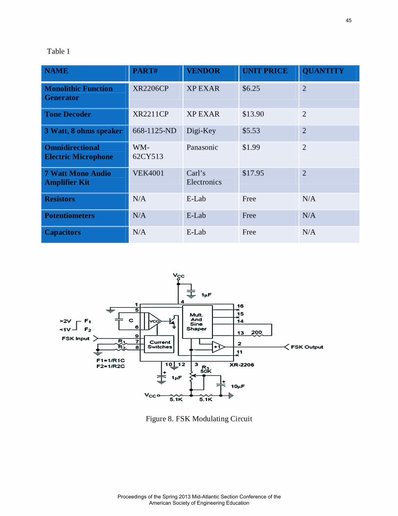
IV. Components and hardware description In this section we focus on the explanation of the design major parts of designed circuits: FSK modulating circuit, power amplifier, and the major part of receiving circuit: FSK demodulating circuit. In the Table 1 is presented the list of components used in building these acoustic modems. The FSK modulating circuit is built around the Monolithic Function Generator XR2206 XR Chip. One of the functions of this chip is that it performs FSK modulation. The chip connections and all circuit components are given in Figure 8.
38
Proceedings of the Spring 2013 Mid-Atlantic Section Conference of the American Society of Engineering Education
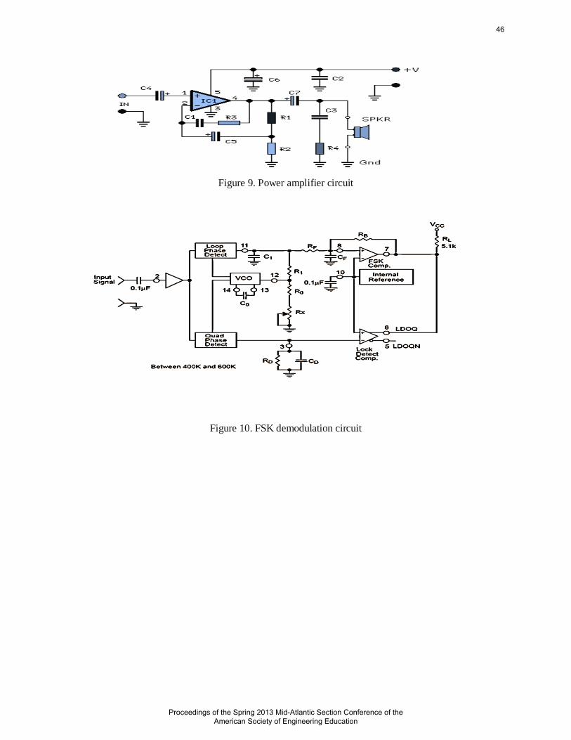
Principle of operation is the following and it is explained is the specification sheet of XR2206 chip [6]: the XR-2206 can be operated with two separate timing resistors, R1 and R2, connected to the timing Pin 7 and 8, respectively, as shown in Figure 8. Depending on the polarity of the logic signal at Pin 9, either one or the other of these timing resistors is activated. If Pin 9 is open-circuited or connected to a bias voltage ≥2V, only R1 is activated. Similarly, if the voltage level at Pin 9 is ≤1V, only R2 is activated. Thus, the output frequency can be keyed between two levels: f1 and f2, as : f1 = 1/R1C and f2 = 1/R2C For split-supply operation, the keying voltage at Pin 9 is referenced to V-. We used the following values: R1= 83kΩ, R2=44kΩ and C=0.01µF. For the power amplifier we have used off the shelf 7 Watt Mono Audio Amplifier Kit[7] . Diagram of this power amplifier is shown in Figure 9. The FSK demodulating circuit is build around Tone Decoder XR 2211CP Chip. One of the functions of this chip is that it performs FSK demodulation. Chip connections and all circuit components can be seen in Figure 10. Detailed principles of operation of XR2211 chip could be found in it’s the specification sheet [8]. A Brief description of the XR-2211 chip is as the following: is a monolithic phase-locked loop (PLL) system especially designed for data communications applications. It is particularly suited for FSK modem applications. It operates over a wide supply voltage range of 4.5 to 20V and a wide frequency range of 0.01Hz to 300kHz. It can accommodate analog signals between 10mV and 3V, and can interface with conventional DTL, TTL, and ECL logic families. The circuit consists of a basic PLL for tracking an input signal within the pass band, a quadrature phase detector which provides carrier detection, and an FSK voltage comparator which provides FSK demodulation. External components are used to independently set center frequency, bandwidth, and output delay. An internal voltage reference proportional to the power supply is provided at an output pin. The XR-2211 is available in 14 pin packages specified for military and industrial temperature ranges [6]. Pin 2 is receiving FSK modulated signal from the microphone. On the pin 7 is the output of the demodulated signal. All other components in figure 9 are found through following equations. These equations are also available in XR-2211 specification sheet. Calculations Mark frequency f1=1200Hz (logical “1”) Space frequency f2=2200Hz (logical “0”) Center frequency f0 = 𝑓1 ∗ 𝑓2 = √1200𝐻𝑧 ∗ 2200𝐻𝑧 = 1624Hz Timing resistor R0, recommended value R0 = 22 kΩ Rx=10 kΩ VCO Center Frequency f0 = 1
𝑅0𝐶0
C0 = 1𝑅0𝑓0
= 122000𝑘Ω∗1624𝐻𝑧
= 27.9nF ≈ 0.022µF Desired tracking bandwidth ∆𝒇 is determined from following equation: ∆𝑓
𝑓0 = 𝑅0
𝑅1
R1 = 𝑅0𝐹0500𝐻𝑧
= 22000𝑘Ω∗1624𝑘𝐻𝑧500𝐻𝑧
= 71.4kΩ ≈ 68kΩ C1 is calculated to determine loop damping C1= 1250∗𝐶0
𝑅1∗∗ , where =0.5 so C1 = 1250∗0.022µF
𝑅1∗0.5∗0.5 =1.61nF
39
Proceedings of the Spring 2013 Mid-Atlantic Section Conference of the American Society of Engineering Education
Rf should be at least five times bigger R1, so Rf > 5R1 = 340kΩ ≈ 400kΩ . Rb should be at least five times bigger Rf so Rb = 5Rf = 2MΩ. Rsum = (𝑅𝑓+𝑅1)𝑅𝑏
(𝑅𝑓+𝑅1+𝑅𝑏) = (400kΩ+68kΩ)2000kΩ
400kΩ+68kΩ+2000kΩ =379.25 kΩ
Cf = 0.25𝑅𝑠𝑢𝑚∗𝐵𝑎𝑢𝑑 𝑅𝑎𝑡𝑒
= 0.25379.25Ω∗1200𝐵𝑎𝑢𝑑
= 0.549nF
Cd > 16∆𝑓
µF = 16200𝐻𝑧
µF = 0.08 µF Rd = 470 kΩ V. Conclusions
The main goal of this project was to design two low cost acoustic modems that communicate in free air and the experimental results are given in this paper. By using the FSK communication schemes, two waves at frequencies of 1.2 kHz (logical “0”) and 2.2 kHz (logical “1”) were generated. Our error was undetectable. There was time delay between transmitted and received signal due to time period of propagation of sound. We have created two prototypes of acoustic modems that can communicate in free air over sound waves that are within human hearing frequency ranges (20Hz – 20kHz). Price of each of these modems was around $50. In the future we want to use these two modems for underwater research.
VI. Acknowledgments
The authors thank for support received from the Department of Defense (DoD) Grant W911NE-11-1-0144.
References: [1] John G Proakis and Masoud Salehi, Fundamentals of Communication System, New York: Pearson Education, 2007. [2] Milica Stojanovic. Underwater Acoustic Communication, Wiley Encyclopedia of Electrical and Electronics Engineering. Boston: Northeastern University. 2008 [3] Desert Star Systems http://www.desertstar.com/Products_product.aspx ?intProductID= 4 [4] B. Benson, Y. Li, R. Kastner. B.Faunce, K. Domond, D. Kimball, C. Schurgers., “Design of a Low-Cost, Underwater Acoustic Modem for Short-Range Sensor Networks”IEEE Embedded Systems Letters, 2010. [5] Greg Malysa and Arseney Romanenko. Acoustic Data Modem http://people.ece.cornell.edu/land/courses/ece4760/FinalProjects/s2010/index.html [6] XR 2206 Monolithic Function Generator http://www.jaycar.com.au/images_uploaded/XR2206V1.PDF [7] Watt Mono Audio Amplifier http://www.electronickits.com/kit/complete/ampl/VEK4001.htm [8] XR 2211 FSK Demodulator/Tone Detector http://www.jaycar.com.au/images_uploaded/XR2211V3.PDF
40
Proceedings of the Spring 2013 Mid-Atlantic Section Conference of the American Society of Engineering Education
Proceedings of the Spring 2013 Mid-Atlantic Section Conference of the American Society of Engineering Education
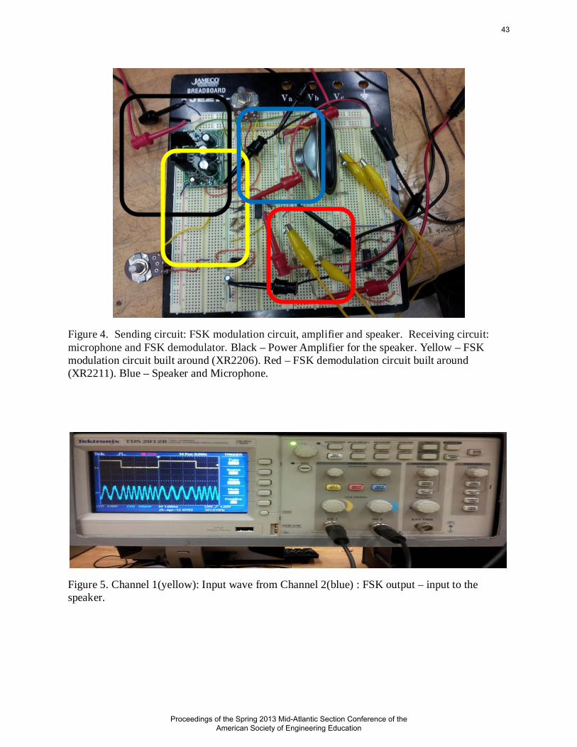
Figure 4. Sending circuit: FSK modulation circuit, amplifier and speaker. Receiving circuit: microphone and FSK demodulator. Black – Power Amplifier for the speaker. Yellow – FSK modulation circuit built around (XR2206). Red – FSK demodulation circuit built around (XR2211). Blue – Speaker and Microphone.
Figure 5. Channel 1(yellow): Input wave from Channel 2(blue) : FSK output – input to the speaker.
43
Proceedings of the Spring 2013 Mid-Atlantic Section Conference of the American Society of Engineering Education
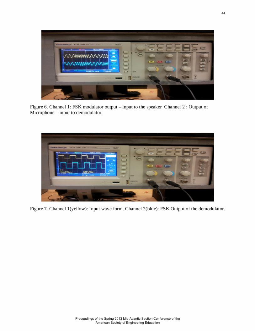
Figure 6. Channel 1: FSK modulator output – input to the speaker Channel 2 : Output of Microphone – input to demodulator.
Figure 7. Channel 1(yellow): Input wave form. Channel 2(blue): FSK Output of the demodulator.
44
Proceedings of the Spring 2013 Mid-Atlantic Section Conference of the American Society of Engineering Education