Low-Density Parity Check Codes for Error Correction in Nanoscale Memory Shalini Ghosh and Patrick D. Lincoln SRI International, Menlo Park, CA September 25, 2007 1 Introduction The continued scaling of photolithographic fabrication techniques down to 32 nanometers and beyond faces enormous technology and economic barriers. Self- assembled devices such as silicon nanowires or carbon nanotubes show promise to not only achieve aggressive dimensions, but to help address power and other gating issues in system architecture, while potentially helping contain rampant increases in fabrication capital costs. However, assembling high-quality, large- scale nanoelectronic circuits (e.g., with Langmuir-Blodgett or related methods) has proven challenging. Among the major challenges are extremely high defect and fault rates in assembled devices. Apart from fabrication errors, nanoscale devices are also more prone to soft errors than microscale devices. Current-day microscale devices (e.g., gates, PLAs, memories) constructed using top-down lithographic techniques have error rates of less than 1% [10]. But computing and storage components built using nanoscale elements (e.g., bistable and switchable organic molecules, carbon nanotubes, single-crystal semiconductor nanowires) may have an order of magnitude higher rates of faults (as high as 10%) [5, 8]. We consider static defects and soft errors separately. Static defects can be handled using testing and reconfiguration [21], though this presents increasing challenges as technology scales. Soft error correction is critical for different nanoscale devices, performing storage (e.g., nanomemory), computation (e.g., nano-ALU) or communication (e.g., nanoscale signal transmitters and receivers). In this paper, we focus on error correction for nanoscale memory. We will concentrate on an architecture that uses nano-PLA blocks and simple nanogates (e.g., majority gate, nand/nor gates) as design components [7]. Because of high soft-error rates, our envisioned nanomemories would also need to employ online error correcting codes (ECCs), as most modern memory subsystems already do [10, 13]. However, for nanomemories with high fault rates, a new type of error correction is desired, since conventional ECC techniques are not directly applicable. The encoders and decoders for Hamming and Hsiao codes, for example, have low encoding and decoding complexity, but also have relatively low error- 1
Transcript
Low-Density Parity Check Codes for
Error Correction in Nanoscale Memory
Shalini Ghosh and Patrick D. LincolnSRI International, Menlo Park, CA
September 25, 2007
1 Introduction
The continued scaling of photolithographic fabrication techniques down to 32nanometers and beyond faces enormous technology and economic barriers. Self-assembled devices such as silicon nanowires or carbon nanotubes show promiseto not only achieve aggressive dimensions, but to help address power and othergating issues in system architecture, while potentially helping contain rampantincreases in fabrication capital costs. However, assembling high-quality, large-scale nanoelectronic circuits (e.g., with Langmuir-Blodgett or related methods)has proven challenging. Among the major challenges are extremely high defectand fault rates in assembled devices. Apart from fabrication errors, nanoscaledevices are also more prone to soft errors than microscale devices. Current-daymicroscale devices (e.g., gates, PLAs, memories) constructed using top-downlithographic techniques have error rates of less than 1% [10]. But computing andstorage components built using nanoscale elements (e.g., bistable and switchableorganic molecules, carbon nanotubes, single-crystal semiconductor nanowires)may have an order of magnitude higher rates of faults (as high as 10%) [5, 8].
We consider static defects and soft errors separately. Static defects can behandled using testing and reconfiguration [21], though this presents increasingchallenges as technology scales. Soft error correction is critical for differentnanoscale devices, performing storage (e.g., nanomemory), computation (e.g.,nano-ALU) or communication (e.g., nanoscale signal transmitters and receivers).In this paper, we focus on error correction for nanoscale memory. We willconcentrate on an architecture that uses nano-PLA blocks and simple nanogates(e.g., majority gate, nand/nor gates) as design components [7]. Because of highsoft-error rates, our envisioned nanomemories would also need to employ onlineerror correcting codes (ECCs), as most modern memory subsystems alreadydo [10, 13]. However, for nanomemories with high fault rates, a new type oferror correction is desired, since conventional ECC techniques are not directlyapplicable.
The encoders and decoders for Hamming and Hsiao codes, for example,have low encoding and decoding complexity, but also have relatively low error-
1
correcting capacity (e.g., Hamming is single error-correcting, double error-detecting).To achieve higher error- correcting capability, codes like Reed-Solomon or BCHrequire more sophisticated decoding algorithms, which would need either (a)complex algebraic decoders that can decode in fixed time – the designs for thesecomplex operations (e.g., floating point operations, logarithms) would be diffi-cult to implement using nanoscale PLAs, which favor simple regular designs, or(b) simpler graphical decoders, that use iterative algorithms (e.g., belief prop-agation) – these typically need need more computation time, and hence wouldnot be fast enough for at-speed ECC operations for nanomemory [16, 4].
For these reasons, we desire an error-correcting system that has (1) higherror detecting and correcting ability, to tolerate relatively high soft error rates;and (2) sparse encoding, decoding and checker circuits, so that they can besynthesized using simple nanoscale hardware. Additional properties that aredesirable for some applications include (a) modular encoder and decoder blocks,which can simplify and shrink hardware design; (b) systematic code structure,which will cleanly partition the information and code bits in the memory; and(c) dynamic error-correcting capability, to enable engineering the trade-off be-tween error correction and system performance. In this report, we focus on theproperty of dynamic error correction.
As the lifetime of a part increases, the faults decrease during the normaloperation of the circuit as compared to the infant mortality rate, and laterincrease again as the part ages. One would typically want the ECC circuitfor the nanomemory to have higher error- correcting capacity during the initialand final stages, but disable unused parts of the ECC encoder/decoder circuitwhile operating at a lower error-correcting rate during normal operation, therebysaving power.
In this paper, we use low-density parity check (LDPC) codes [12] for ECCin nanomemories. We propose the use of a variant of a particular type of LDPCcode, Euclidean Geometry (EG) LDPC [16], which is built using special struc-tures of finite Euclidean Geometry. Various types of EG-LDPC codes have thedifferent properties listed before, e.g., type-I codes are systematic, type-II codeshave encoding and parity check matrices with regular modular structure, Gal-lager codes have properties that enable their error correction rate to be changeddynamically. More details about these codes and their properties are given inSections 3 and 4. The sparseness (enabling low fan-in circuit implementation)and low computational overhead of decoding EG-LDPC codes make them easyto implement using nanoscale hardware.
Various nanodevices have been proposed in the literature (e.g., nanowire-based PLA, quantum nanodots) to serve as the basic building block of memoryand computation elements. In this paper, we propose the design of a nanomem-ory array using nanowire-based-PLA components [9]. We analyze the propertiesof EG-LDPC codes that make it suitable as ECC for nanomemory, and suggesthow the coder and decoder circuits can be efficiently fabricated using nano-PLAmemory units and gates. We also consider that the encoder and checker circuitsthemselves can suffer faults, since they may be fabricated out of fault-pronenanoscale components. We provide an analysis of fault detection and correction
2
capacities of nanomemories with EG-LDPC codes, and design an overall systemarchitecture based on nano-PLA building blocks.
2 Background
We outline concepts that will be useful in understanding our main design andarchitecture for ECC in nanomemory based on EG-LDPC codes.
2.1 LDPC codes
LDPC codes have several advantages, which have made them popular in manycommunication applications: (1) low density of the encoding matrix, (2) easyiterative decoding, (3) generating large code words that can approach Shannon’slimit of coding [16].
An LDPC code is defined as the null space of a parity check matrix H thathas the following properties [16]:
1. Each row has ρ number of 1’s.
2. Each column has γ number of 1’s.
3. The number of 1’s that are common between any two columns (λ) is nogreater than 1, i.e., λ = 0 or 1.
4. Both ρ and γ are small compared to the length of the code and the numberof rows in H .
As both ρ and γ are very small compared to the code length and the numberof rows in the matrix H , H has a low density of 1’s. Hence H is said to be a low-density parity check matrix and the code defined by H is said to be a low-densityparity check code.
The density of H (r) is defined to be the ratio of the total number of 1’s inH to the total number of entries in H — in this case r = ρ/n = γ/J , where J isthe number of rows in H . This kind of LDPC code is said to be a (γ, ρ)-regularLDPC code. If the weights of all the columns or rows in H are not the same,then it is called an irregular LDPC code.
2.2 EG-LDPC codes
In recent work [26], Euclidean Geometry (EG) constructions over GF (2s) havebeen used to construct H-matrices for LDPC codes. Using EG(m, 2s), whereeach point in the geometrical space can be represented by an m-tuple overGF (2s), the H-matrix can be interpreted as an incidence matrix – every col-umn of the matrix represents a point in this space, every row represents a line,and every entry of 1 in the matrix represents that the corresponding row lineis incident on the column point. Figure 1 shows an example of the EG-LDPC
3
code. This connection to finite Euclidean Geometry has advantages for our ap-plication:
(1) Using the structure of EG(m, 2s), the LDPC H-matrices can be con-structed quite efficiently, since this matrix has some useful properties. Forexample, for the Gallager code (see Section 3 for details), every Hi componentin the matrix represents a set of parallel lines (a bundle), which can be easilyenumerated using Galois Field (GF) operations. This obviates the necessity of asearch algorithm for designing the H-matrix. Instead, for any size of the mem-ory, we can design the corresponding H-matrix efficiently using GF operations.Similar advantages exist in constructing other EG-LDPC codes, e.g., type I,type II
(2) The regular geometric structure makes the corresponding LDPC codedecodable using a multistep majority decoder, thus making it unnecessary tohave iterative decoders [16]. As outlined in Section. 1, this is one of the proper-ties we desire in ECC for nanomemory, to make the decoding fast and therebyhave low latency overhead for normal memory load/store operations.
Figure 1: Euclidean Geometry and the corresponding EG-LDPC H matrixformed from the incidence matrix of the lines on the points in the geometry.
4
2.3 Decoding
Since EG-LDPC is a finite geometry cyclic code [16], it can be decoded effec-tively using one-step majority logic (ML) decoding. Here, we explain how thatdecoding is performed.
Let the n-bit faulty code word r be the sum of the original code word c andthe error word e, where e is 1 at the locations at which the errors/faults haveoccurred, 0 otherwise:
r = c + e.
To find whether a particular error bit ei is 1 or 0, the decoder first calculatesparity equations, each of which calculates a check sum on some bits of r. Aset of J parity equations is orthogonal on ei if each of the J parity equationscheck ei (i.e., ei is included in the check sum of each parity equation), but noother error bit is checked by more than one parity equation. If a set of J parityequations is orthogonal on ei, the ML decoding rule can be applied to decodeei: ei is decoded to 1 if the majority of the parity check sums of the J checksums is 1, otherwise ei is 0.
In EG-LDPC, for every bit position i there is a set of γ rows Ai in H thatis orthogonal on i, where
Ai = {hi1, . . . ,hi
γ},
i.e., the ith component of each row in Ai is 1 and two rows in Ai have a common1 in no other positions. This signifies that the error bit in the ith position is MLdecodable. For the ith bit position, a set of γ syndrome equations Si is formedusing the rows in Ai, where
Si = {sij = e.hi
j : hij ∈ Ai, for 1 ≤ j ≤ γ}
Correct decoding of ei using the ML decoding rule, applied on the outputs ofthe syndrome equations Si, is guaranteed if the number of errors in e is lessthan γ/2. This can be repeated for every bit position i to estimate the errorword e.
In this paper, we consider one-step ML decoding. However, the perfor-mance of the hard-decision one-step ML decoding can be further improved us-ing Gallager’s iterative bit-flipping (BF) algorithm [12], which is able to correcterrors when the number of errors exceeds γ/2. BF uses simple comparison,sum, and majority operations and is therefore easier to implement using nano-PLAs than the popular sum-product algorithms for decoding LDPC codes usingbelief-propagation, which requires real-number arithmetic and computation oflogarithms.
2.4 Nano-PLA Architecture
In this work, we refer to the nanoarchitecture based on Programmable LogicArrays (PLAs), as proposed by Dehon et al. [7]. He proposes to build a two-plane PLA with silicon nanowires. Figure 2 shows the proposed architecture.Nanowires can be aligned closely in a single orientation with the help of flow
5
techniques and then they can be rotated and repeated so that multiple layersof nanowires form crossbar arrays with switchable diodes at the crosspoints.These arrays can serve as memory cores, programmable wired-OR planes, andprogrammable crossbar interconnect arrays. As Figure 2 shows, the architectureis a combination of two coupled NOR-NOR planes, which can be also regardedas AND-OR PLA using DeMorgan’s Laws and complementation. In Figure 2each of the two interconnected logic planes consists of a programmable wired-OR array followed by two restoration arrays; the first inverts the OR logicand the second serves as a noninverting buffer. Stochastic decoders are formedusing vertical microscale wires A0-A3, which address the horizontal nanowires.Overall, this simple PLA structure serves as a universal logic structure as itsupports AND, OR, and NOT operations.
Figure 2: Nano-PLA architecture [7].
The defects that occur in this kind of architecture are mainly of two types– (1) wire, where the wire is either functional or defective and (2) non pro-grammable crosspoint, where the crosspoint cannot be programmed into the onstate, or the crosspoint may be shorted into an on state. For static defects,Naemi et al. [21] proposed a greedy algorithm for mapping a logic function ona nano-PLA with defective nanowires. In this work, we consider how dynamicerrors can be handled using ECC.
3 Dynamic LDPC in Nanomemory
Dynamic ECC is a property of EG-LDPC codes that we will explore here in de-tail. We begin by outlining the motivation for having dynamic codes in nanoar-chitectures.
6
3.1 Motivation
Soft error rates vary over the lifetime of complex electronic components. The“bathtub curve” of failure rates classically begins with a very high rate of infantmortality, then smooths to a relatively low rate of failure for some period of time,and then slowly rises toward the end of the life cycle. In addition, environmentalstresses may change the expected fault rate (e.g., temperature, radiation levels,nearby radio transmission). Classically, one must design error correcting codes(ECCs) to tolerate the maximum failure rate expected over the entire lifetimeof a device, resulting in “wasteful” tolerance of “too many” faults during thebulk of the component’s lifetime.
At the highest level, the work presented here aims to enable controlled reduc-tion in fault tolerance during a part’s lifetime. More precisely, we work towardenabling the engineering of defect and fault tolerance, traded against systempower and other key parameters. For example, if we are able to diagnose andreconfigure out subcomponents after a time of high-fault-rate infant mortality,and we expect fault arrival rates to be greatly reduced for a significant period oftime, we would like to turn off some of the power-hungry ECC circuits. Later, iffault rates were to climb again, we would wish to turn those ECC circuits backon.
In some cases, fault arrival rates are predictable. Some device families showa bathtub curve of fault arrival rates fairly smoothly [10]. In some systems, faultrates follow a mission profile (e.g., altitude), and in others fault rates are stronglyaffected by easily observable environmental conditions (e.g., temperature). Also,if a system is able to detect the frequency and severity (number of bits) of errorsin encoded words, and fault rates change slowly (with respect to clock cycle),then the system may be able to predict future fault rates to some degree. Inthese cases, we wish to enable the dynamic control of fault tolerance, which mayallow one to shut down a subset of ECC circuits to save power.
3.2 Proposed Approach
For dynamic ECC, we will use a particular type of LDPC code – Gallager code– which is the original LDPC code proposed by Gallager [12]. The advantage ofthis code is that the decoding parity check matrix (H-matrix) of this code canbe expressed in a special form:
HT = (HT1
HT2
. . . HTγ ), (1)
where H1 is a matrix in the standard systematic form [I : A] [4], and H2, . . . , Hγ
are permutations of H1. A (γ, ρ)-regular Gallager code has a parity check matrixwith column weight γ and row weight ρ, and can correct as many as γ/2 errors.The number of rows in the H-matrix is J = k × γ, and the number of columnsis n = k × ρ.
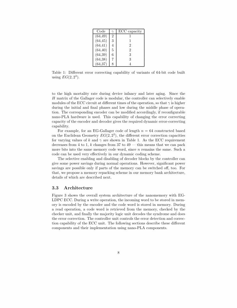
In dynamic ECC, one would typically want the ECC circuit for the nanomem-ory to have higher error correcting capacity during the initial and final stages,since faults decrease during the normal operation of the circuit as compared
Table 1: Different error correcting capability of variants of 64-bit code builtusing EG(2, 23).
to the high mortality rate during device infancy and later aging. Since theH matrix of the Gallager code is modular, the controller can selectively enablemodules of the ECC circuit at different times of the operation, so that γ is higherduring the initial and final phases and low during the middle phase of opera-tion. The corresponding encoder can be modified accordingly, if reconfigurablenano-PLA hardware is used. This capability of changing the error correctingcapacity of the encoder and decoder gives the required dynamic error-correctingcapability.
For example, for an EG-Gallager code of length n = 64 constructed basedon the Euclidean Geometry EG(2, 23), the different error correction capacitiesfor varying values of k and γ are shown in Table 1. As the ECC requirementdecreases from 4 to 1, k changes from 37 to 49 — this means that we can packmore bits into the same memory code word, since n remains the same. Such acode can be used very effectively in our dynamic coding scheme.
The selective enabling and disabling of decoder blocks by the controller cangive some power savings during normal operations. However, significant powersavings are possible only if parts of the memory can be switched off, too. Forthat, we propose a memory repacking scheme in our memory bank architecture,details of which are described next.
3.3 Architecture
Figure 3 shows the overall system architecture of the nanomemory with EG-LDPC ECC. During a write operation, the incoming word to be stored in mem-ory is encoded by the encoder and the code word is stored in memory. Duringa read operation, a code word is retrieved from the memory, checked by thechecker unit, and finally the majority logic unit decodes the syndrome and doesthe error correction. The controller unit controls the error detection and correc-tion capability of the ECC unit. The following sections describe these differentcomponents and their implementation using nano-PLA components.
8
Figure 3: Overall architecture of ECC nanomemory.
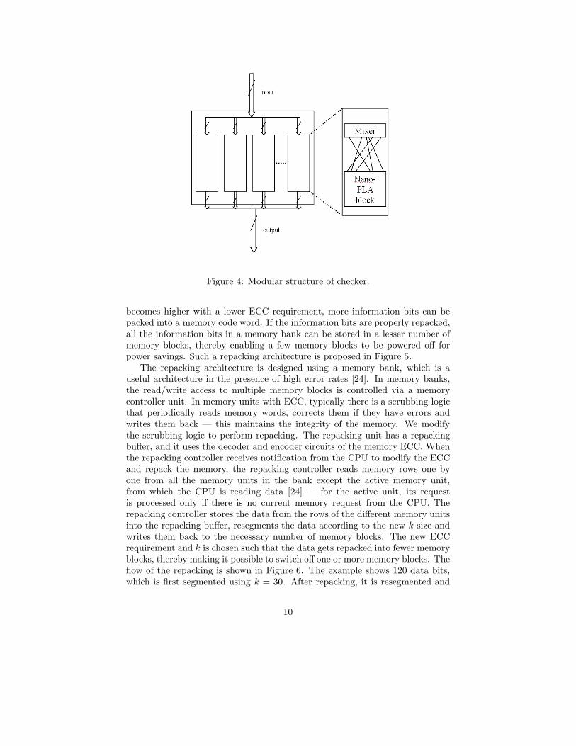
3.3.1 Checker and Encoder
According to Section 3.2, each submatrix Hi in Equation 1 can be expressed inthe form PiH1, where Pi is a permutation matrix. Figure 4 shows the modulardesign of the checker circuit, the hardware implementation of the parity checkmatrix H . The ith unit in the checker corresponds to the circuit for Hi, andconsists of a block of XOR gates implementing H1 and a reconfigurable permu-tation block configured to implement PT
i . If the system needs to operate at anerror-correcting level of γ/2, encoder units 1 to γ are enabled by a controller andthe remaining units are disabled. The design of the checker can be implementedusing the same module H1 in each unit, along with a corresponding permutingarray (mixer) – this makes the design regular and modular, both of which arecharacteristics facilitating implementation using nano-PLA components. Thebasic block H1 is essentially a set of n-input XOR gates, which can be realizedin nano-PLA using a nested tree configuration of the 2-input XOR gates out-lined in Section 2.4. The permutation array is a reconfigurable switching circuit,which can be implemented using a nano-PLA cross-bar architecture [7].
Once the checker circuit is changed by selectively turning off some of itsblocks, the corresponding encoder circuit can be modified by reconfiguring thenano-PLA implementing the encoder [7].
3.3.2 Memory
When the ECC requirements are less, the k value of the code can be increased(thereby decreasing γ). As shown in Table 1, the k value can be initially setto a low number (e.g., 37), so that we get high ECC in the memory. Later,as the memory ECC requirements decrease, the k value can be increased toa higher number (e.g., 49). In terms of the memory, changing k amounts tovarying the number of information bits stored per word of memory. When k
9
Figure 4: Modular structure of checker.
becomes higher with a lower ECC requirement, more information bits can bepacked into a memory code word. If the information bits are properly repacked,all the information bits in a memory bank can be stored in a lesser number ofmemory blocks, thereby enabling a few memory blocks to be powered off forpower savings. Such a repacking architecture is proposed in Figure 5.
The repacking architecture is designed using a memory bank, which is auseful architecture in the presence of high error rates [24]. In memory banks,the read/write access to multiple memory blocks is controlled via a memorycontroller unit. In memory units with ECC, typically there is a scrubbing logicthat periodically reads memory words, corrects them if they have errors andwrites them back — this maintains the integrity of the memory. We modifythe scrubbing logic to perform repacking. The repacking unit has a repackingbuffer, and it uses the decoder and encoder circuits of the memory ECC. Whenthe repacking controller receives notification from the CPU to modify the ECCand repack the memory, the repacking controller reads memory rows one byone from all the memory units in the bank except the active memory unit,from which the CPU is reading data [24] — for the active unit, its requestis processed only if there is no current memory request from the CPU. Therepacking controller stores the data from the rows of the different memory unitsinto the repacking buffer, resegments the data according to the new k size andwrites them back to the necessary number of memory blocks. The new ECCrequirement and k is chosen such that the data gets repacked into fewer memoryblocks, thereby making it possible to switch off one or more memory blocks. Theflow of the repacking is shown in Figure 6. The example shows 120 data bits,which is first segmented using k = 30. After repacking, it is resegmented and
10
Figure 5: Memory repacking architecture.
repacked with k = 40. This enables shutting of memory bank #4, as n remainsthe same.
3.3.3 Decoder and Controller
The majority-logic (ML) decoder requires two key hardware units: XOR andmajority (MAJ). A 3-input majority gate MAJ(A,B,C) can be implementedusing the AND-OR planes of the nano-PLA, since MAJ(A,B,C) = AB + BC +AC. An n-input MAJ gate can be similarly implemented using AND/OR gates,or equivalently using the AND-OR planes of a nano-PLA. Like the encodercircuit, the decoder is also reconfigured when the ECC is modified, to handledynamic coding. This reconfiguration can be handled easily since the MAJdecoder is implemented using reconfigurable nano-PLA.
The control signals from the memory repacking controller circuit (used todisable memory blocks in the bank architecture) are also used for selectivelyenabling and disabling modules of the checker, and for reconfiguring the encoderand checker components. Since we need only one controller for a completememory bank, this module can be implemented using micro-level circuitry.
4 Other Properties of LDPC in Nanomemory
Apart from dynamic ECC, other properties are desirable in ECC for nanomem-ory designs in particular application domains. We outline two such properties
11
Figure 6: Flow of memory repacking.
and the corresponding EG-LDPC codes.
4.1 Systematic Codes
In systematic codes, the G matrix is of the form [I : P ], where I is an identitymatrix. This simplifies the encoding procedure – during encoding, the paritybits can simply be concatenated to the message bits to create a code word.
One particular type of EG-LDPC code, the two-dimensional type-I (0, s)-th order code [16], is a cyclic code. Any cyclic code can be converted to anequivalent systematic form [25], which implies that a 2d type-I EG-LDPC codecan be expressed in systematic form. The 2d type-I EG-LDPC code has someother advantages – since it is a cyclic code, each row of the H matrix canbe obtained by cylically shifting the previous row. Hence, the decoder can beefficiently implemented in hardware using a cyclic shift register [16, 2], as shownin Figure 7.
The 2d type-I EG-LDPC code can be generated easily using Euclidean Ge-ometry. For the code with length n = 22s−1, number of parity bits n−k = 3s−1and dimension k = 22s − 3s, the corresponding Euclidean Geometry EG(2, 2s)consists of 22s − 1 lines that do not pass through the origin. The H matrix,which is the incidence matrix of this EG, is a (22s−1)× (22s−1) square matrix,where each row can be created by cyclically shifting the first row and the rowweight (ρ) is equal to the column weight (γ). Choosing s = 3, we get n = 63,k = 37 and ρ = γ = 16, which means that this code can be used in a 64-bit
12
Figure 7: Cyclic shift register-based decoder for EG-LDPC type-I code.
memory architecture (one additional bit can be packed with an overall parity)requiring systematic encoding and capacity of correcting 8 errors per word.
4.2 Modular Codes
A desirable property in some nanomemory applications is modularity of hard-ware design of encoder and decoder. This makes the hardware design quitesimple, since one can optimize the design of a single module and use multiplesuch modules to create both the encoder and the decoder circuits.
We will show how a particular class of EG-LDPC code, type-II, has thisdesirable modularity property. Type-II EG-LDPC codes are quasi-cyclic, i.e.,each row of their H-matrix can be obtained by shifting previous rows by aparticular fixed number of positions c (if c = 1, the code is cyclic ⇒ cycliccodes are a special case of quasi-cyclic codes). Now, any quasi-cyclic matrix canbe equivalently put in a circulant form, where the H- matrix comprises a setof circulants [15]. Note that a circulant is a square matrix where each row isa cyclic shift of the row above it (with wraparound of the top row), and eachcolumn is a cyclic shift of the column to its left (with wraparound of the leftmostrow). A detailed example of quasi-cyclic codes, circulants, and the equivalencebetween these two is shown in Figure 8. Recent work has shown that the encodermatrix can also be obtained in modular form for certain specific kinds of type-IIcodes [11].
13
Figure 8: Quasi-cyclic H matrix and corresponding circulant form, for type-IIEG-LDPC code.
5 Analysis and Experiments
We analyze the effects of faults and dynamic coding in the various componentsof the model outlined in Section 3.3.
5.1 Fault Tolerance
Let ǫe, ǫm and ǫc be random variables signifying the number of errors in theencoder, memory, and checker blocks, respectively. According to Section 3.3.3,when γ components are enabled by the controller, the overall error correctingcapacity of the ECC memory system (with ML decoding) is γ/2. Therefore, themajority-logic decoder will be able to correct errors as long as
ǫe + ǫm + ǫc ≤ γ/2. (2)
Note that the MAJ decoder is assumed to be fault free, which can be ensuredby using self-checking in the MAJ logic.
Let us now analyze each component of the above equation in detail. Whenγ units are enabled by the controller, the code is a (γ, ρ)-regular Gallager codeaccording to Section 3.2, i.e., the check matrix unit H1 has a single 1 in eachcolumn and ρ 1’s in each row. Consequently, each XOR gate realizing the H1
matrices are ρ-input XOR gates. In this analysis, we will consider the effects
14
2 4 6 8 10 12 14 160
0.1
0.2
0.3
0.4
0.5
0.6
0.7
0.8
0.9
1
Gamma
Pro
babi
lity
of C
orre
ct O
pera
tion
n = 32
n = 16
n = 8
Figure 9: Probability of correct detection as a function of the number of dynamicEG-LDPC checker units (γ) utilized. The three plots correspond to differentvalues of the memory size (n = 8, 16, 32), corresponding to different values ofthe m parameter (m = 3, 4 and 5, respectively) of the EG-LDPC code.
of errors in the XOR gates to be additive. In some cases errors can mask eachother, e.g., complementary soft errors in two inputs of an XOR gate can maskeach other – we do not consider that in this worst-case analysis.
Let pe and pc be the errors in one bit location of an XOR gate in the encoderand checker, respectively, and pm be the probability of a nano-PLA memoryjunction losing its charge. Assuming errors to be i.i.d. and the total number ofcode bits to be n, we get
Prob(e out of n code bits have errors) =
(
n
e
)
(p)e(1 − p)n−e, (3)
where putting p = pj gives us the error probability in the memory, while select-ing p = pe gives us the error probability in the encoder or checker. ConsideringEquations (2) and (3), we see that the distribution of errors in the overall ECCmemory system is the sum of binomial random variables. Therefore, the prob-ability of the majority decoder not having any error is given by the cumulativedistribution of the convolution of binomial distributions.
Figure 9 shows how the probability of error-free operation of a memorysystem with EG-LDPC error correction changes along with different values ofγ (the number of stages in the dynamic error control), for pe, pc = 1% (errorrates for encoder and checker) and pm = 2% (error rate for memory). As shownin the figure, for an 8-bit memory, γ = 6 gives almost 100% probability ofcorrect operation; the same high reliability is obtained using γ = 8 for a 16-bit memory and γ = 12 for a 32-bit memory. Figure 10 shows the plot for a64-bit memory (corresponding to m = 6), for a higher error rate (8%) — usingγ = 32 in this case gives > 99% probability of correct operation. Note that
15
0 5 10 15 20 25 30 350
0.1
0.2
0.3
0.4
0.5
0.6
0.7
0.8
0.9
1
Gamma
Pro
babi
lity
of C
orre
ct O
pera
tion
Figure 10: Probability of correct detection as a function of the number of dy-namic EG-LDPC checker units (γ) utilized. The plot corresponds to memorysize n = 64, corresponding to m = 6 for the EG-LDPC code.
using Gallager’s bit-flipping algorithm (as discussed in Section 3.2) can give ussimilar probability of correct operation with lesser γ (and hence a lesser numberof hardware component modules), at the cost of more complex hardware in eachmodule. Note that in all these figures, the size of the memory is n = 2m, for a(m, 2s) EG-LDPC code.
5.2 Dynamic Coding
Along the bathtub curve, the probability of failure of components varies —high in the beginning, low during normal operations, and finally high again.Figure 11 shows how the γ value required (for > 99% probability of normaloperation) varies with changing probability of failure of each component (inthis case, we assume m = 5 and p = pe = pd = pc = pm). When p = 0.06, therequired γ = 15, but as p decreases to 0.01, γ decreases steadily to 5.
Figure 12 shows a simulation of the bathtub curve of failure – initially,during infant mortality failure, a high value of γ is required. During the middlephase, when there is a low constant failure rate, the γ required is less, so thatsome of the components of the checker and memory bank can be disabled,leading to savings in static power dissipation. Toward the end of the devicelifetime, when wearout failures increase the error rate, the required γ increasesagain, leading to increased power dissipation. This demonstrates that for lowerprobability of component failure, we can selectively disable the blocks in thechecker and memory bank and obtain substantial power savings. Thus, dynamicerror correction is well suited in this domain.
16
0.01 0.02 0.03 0.04 0.05 0.065
6
7
8
9
10
11
12
13
14
15
Probability of failure
Gam
ma
Figure 11: Change of γ (for correct operation of the ECC memory with > 99%probability) with different values of p.
0 5 10 15 20 25 3055
60
65
70
75
80
85
90
95
100
Time
Per
cant
age
of m
axim
um p
ower
dis
sipa
ted
Figure 12: Percentage of maximum power dissipated (for correct operation ofthe ECC memory with > 99% probability) along the bathtub curve of failure.
17
Memory size Memory Area Info Area Parity + ECC Area Overhead1K 384K 240K 188K 49%2K 768K 480K 332K 43%4K 1536K 960K 620K 40%8K 3072K 1920K 1196K 39%16K 6144K 3840K 2348K 38%
Table 2: Area overhead for LDPC-ECC in nanomemory
6 Area Overhead
The different components of the memory LDPC-ECC system implemented usingnanocomponents are (1) encoder, (2) memory, (3) checker, and (4) decoder.Note that the controller is designed using micro-level circuitry for the wholememory bank; hence, we do not consider its area in our current analysis.
An upper bound on the number of 2-input XOR gates required for the en-coder and checker circuits is (n − k)(k − 1) + J(ρ − 1). The decoder has nγ-input MAJ gates, which can be synthesized using 2-input AND/OR gatesor directly with a nano-PLA. In either case, each of the n γ-input MAJ gateswill need on the order of (2γ−1) 2-input AND gates and (γ − 1) 2-input ORgates. Let us consider that a memory unit is composed of 6 nanotransistors,while 2-input OR, AND, and XOR gates are composed of 4, 4, and 8 nanotran-sistors respectively [20]. For a 2-dimensional (64, 40) EG-Gallager code withγ = 6, ρ = 6, J = 64, constructed based on the Euclidean Geometry EG(2, 23),the area of the encoder, checker and decoder circuits is 44K transistors. Thecorresponding area for a 64-bit memory with 1K rows is 384K transistors. Ta-ble 2 shows the area overhead of having LDPC-ECC in the memory, wherearea is measured in terms of number of transistors. As the size of the memoryblock increases, the overhead of the parity bits and the ECC logic convergesto (1 − coderate) = (n − k)/n = 37.5%, which indicates that for large memoryblocks the overhead due to the ECC encoder, checker, and decoder circuits isvery low (e.g., for 16K memory, it is 0.5%). This is consistent with observationsby other researchers on other types of LDPC codes [20].
7 Irregular LDPC Codes
There are different types of LDPC codes where the number of 1’s in the rows andcolumns are not uniform — some of these irregular codes have the propertiesof modular, systematic, and dynamic codes that we have been studying in thispaper. For example, Accumulate-Repeat-Accumulate (ARA) codes [2], whichare constructed by suitably repeating core protograph structures, can have bothmodular encoder and decoder matrices. The same property holds for Cycle-invariant Difference Set (CIDS) codes, which are generated using difference setsover Abelian groups and have block-circulant structure of both encoder and
18
decoder matrices [18]. Both these codes can be used as dynamic codes —however, they are not well suited for our nano-PLA-based architecture, sincethese codes are not MAJ-logic decodable and need belief propagation-baseddecoders, which are significantly more complex to implement in nanohardware.
8 Related Work
LDPC codes have been widely used in different communication applications [16],especially after Mackay’s recent work revived interest in them [17]. In our work,we use a property of EG-LDPC codes that allows simpler decoding logic (in-volving majority gates) to be used, which can be implemented in nanohardwareusing different techniques [3]. LDPC codes defined over other finite geometrieshave been studied lately [26], and hardware for performing efficient decoding ofLDPC codes has been proposed [6, 19].
The work in this paper is focused on ECC for nanomemory. Other error-correcting codes have been used at nanoscale – recently a hierarchical faulttolerance technique, using Hamming codes, was proposed for nanocomputingoperations [23].
One aspect of our current work is that the ECC circuit components them-selves can have faults in them, which must be accounted for during error cor-rection. Another scheme for handling faulty hardware modules was consideredin von Neumann’s seminal fault-tolerant multiplexing scheme [29], which hasalso been extended recently using a probabilistic computation model with noisygates [22]. In micro-level circuits, various other fault tolerance techniques havebeen used, e.g., total self-checking [1, 27], parity prediction [28].
9 Conclusions and Future Work
We want to focus on several interesting extensions to this work. If there areline-level faults in the address lines or row/column lines, then it is useful to haveblock-level error correcting codes like Reed-Solomon [16] instead of LDPC. Ifthe whole memory block becomes unusable because of a fault, then it is use-ful to have distributed error correction in different memory blocks instead of acentralized error-correcting scheme. To that effect, we intend to explore stripedRAID-type architecture for nanomemory banks [14]. In the nanodomain, asym-metric and unidirectional faults might occur – we plan to investigate such errormodels, study the prevalence of these types of errors through fault simulationsin models of nanocomputing, and handle such faults using corresponding error-correcting codes, e.g., asymmetric codes, unidirectional codes [4]. Finally, wewant to implement an actual prototype of the proposed architecture on thenano-PLA substrate and perform experiments with actual memory traces fromdifferent domains [13], injecting faults following different fault models.
19
References
[1] D. A. Anderson and G. Metze. Design of totally self-checking checker form-out-of-n codes. IEEE Trans. on Computers, C-22, March 1973.
[2] K. Andrews, S. Dolinar, and J. Thorpe. Encoders for block-circulant ldpccodes. In ISIT, 2005.
[3] V. Beiu, S. Aunet, J. Nyathi, R. R. Rydberg-III, and A. Djupdal. The van-ishing majority gate trading power and speed for reliability. In Proceedingsof NanoArch, 2005.
[4] R. E. Blahut. Theory and Practice of Error Control Codes. Addison-Wesley,1983.
[5] M. Butts, A. DeHon, and S. C. Goldstein. Molecular electronics: Devices,systems and tools for gigagate, gigabit chips. In Proceedings of the Inter-national Conference on Computer-Aided Design, pages 433–440, November2002.
[6] S.-C. Chae and Y.-O. Park. Low complexity encoding of regular low densityparity check codes. In Proceedings of VTC, 2003.
[7] A. Dehon. Nanowires-based programmable architectures. ACM Journal onEmerging Technologies in Computing Systems, 1(2):109–162, July 2005.
[8] A. Dehon and H.Naeimi. Seven strategies for tolerating highly defectivefabrication. In IEEE Design and Test of Computers, volume 22, pages306–315, July-August 2005.
[9] A. DeHon and K. Likharev. Hybrid cmos/nanoelectronic digital circuits:devices, architectures, and design automation. In ACM/IEEE InternationalConference on Computer-Aided Design (ICCAD), pages 375–382, 2005.
[10] D. Edenfeld, A.B. Kahng, M. Rodgers, and Y. Zorian. 2003 technologyroadmap for semiconductors. Computer, 37(1):47–56, Jan 2004.
[11] W. Fong. White paper for low density parity check (ldpc) codes for ccsdschannel coding blue book. In CCSDS P1B Channel Coding Meeting, Hous-ton, TX, 2002.
[12] R. G. Gallager. Low Density Parity Check Codes. PhD thesis, MIT, 1960.
[13] S. Ghosh, S. Basu, and N. A. Touba. Selecting error correcting codesto minimize power in memory checker circuits. Journal of Low PowerElectronics, 1(1):63–72, April 2005.
[14] J. L. Hennessy and D. A. Patterson. Computer Architecture: A Quanti-tative Approach (The Morgan Kaufmann Series in Computer Architectureand Design). Morgan Kaufmann, 2002.
20
[15] C. R. Johnson. Matrix Theory and Applications. American MathematicalSociety, 1990.
[16] S. Lin and D.J. Costello Jr. Error Control Coding. Pearson Prentice Hall,2004.
[17] D. J. C. Mackay. Comparison of constructions of irregular Gallager codes.IEEE Trans. Commun., 47(10), 1999.
[18] O. Milenkovic, I.B. Djordjevic, and B. Vasic. Block-circulant low-densityparity-check codes for optical communication systems. IEEE Journal ofSelected Topics in Quantum Electronics, 10(2), 2004.
[19] G. Murphy, E. M. Popovici, R. Bresnan, W. P. Marnane, and P. Fitzpatrick.Design and implementation of a parameterizable LDPC decoder IP core.In Proceedings of International Conference on Microelectronics, 2004.
[20] H. Naeimi. Personal communication. 2007.
[21] H. Naeimi and A. Dehon. A greedy algorithm for tolerating defective cross-points in nanopla design. In Proceedings of the International Conferenceon Field-Programmable Technology, pages 49–56, December 2004.
[22] Y. Qi, J. Gao, and J.A.B. Fortes. Probabilistic computation: A generalframework for fault tolerant nanoelectronic systems. Technical report, Uni-versity of Florida, Gainesville, Florida, 2003.
[23] W. Rao, A. Orailoglu, and R. Karri. Architectural-level fault tolerant com-putation in nanoelectronic processors. In 2005 International Conference onComputer Design, pages 533–542, 2005.
[24] A.M. Saleh, J.J. Serrano, and J.H. Patel. Reliability of scrubbing recovery-techniques for memory system. IEEE Transactions on Reliability, 39(1),1990.
[25] P. Sweeney. Error Control Coding: From Theory to Practice. John Wileyand Sons, 2002.
[26] H. Tang, J. Xu, Y. Kou, S. Lin, and K. A. S. Abdel-Ghaffar. On algebraicconstruction of gallager and circulant low-density parity-check codes. IEEETransactions on Information Theory, 50(6):1269–1279, June 2004.
[27] D. L. Tao, C. R. P. Hartmann, and P. K. Lala. A general technique fordesigning totally self-checking checker for 1-out-of-n code with minimumgate delay. IEEE Transactions on Computers, 41(7), July 1992.
[28] N. A. Touba and E.J. McCluskey. Logic synthesis techniques for reducedarea implementation of multilevel circuits with concurrent error detection.In Proc. of ACM/IEEE International Conference on Computer-Aided De-sign (ICCAD), pages 651–654, 1994.
21
[29] J. von Neumann. Probabilistic logics and the synthesis of reliable organizmsfrom unreliable components. Automata Studies, pages 43–98, 1956.