IEEE TRANSACTIONS ON MAGNETICS, VOL. 57, NO. 8, AUGUST 2021 4200407
Low-Energy Picosecond Magnetic Switching forSynthetic Ferrimagnetic Free Layer Utilizing
the Electric-Field-Tuned RKKY EffectLei Wang , Xuesong Zhou, Runzi Hao , and Tai Min
Center for Spintronics and Quantum Systems, State Key Laboratory for Mechanical Behavior of Materials,Xi’an Jiaotong University, Xi’an, Shaanxi 710049, China
The precessional switching mechanism has governed the magnetic switching in magnetic tunnel junctions (MTJs) in thesub-nanosecond range, which exponentially increases the switching current density of magnetic random access memory (MRAM).Thus, there needs to be an alternative switching mechanism with much higher energy efficiency to bring down the switchingcurrent density significantly and make the MRAM compatible with high-speed L1/2—static random access memory (SRAM) atsub-nanosecond range. Using the recent discovered external electric field (E-field) tunable Ruderman–Kittel–Kasuya–Yosida (RKKY)phenomena in a synthetic ferrimagnet (E-SFi), we propose a totally different Chrysanthemum-like switching mechanism to realize alow-energy picosecond writing MRAM design, which breaks the precessional switching mechanism at picosecond region. And ourresults show that the critical switching current density can be significantly reduced by one order of magnitude compared to thatof a conventional MTJ design down to 100 ps. In addition, we study the robustness of the asynchronous conditions between thecharge current pulse and the E-field pulse for its practical applications.
Index Terms— Low switching current, magnetic random access memory (MRAM), picosecond magnetic switching,Ruderman–Kittel–Kasuya–Yosida (RKKY) interaction, synthetic ferrimagnet.
I. INTRODUCTION
BECAUSE of its nonvolatility, high speed, and high den-sity, magnetic random access memory (MRAM) has
received extensive attention in both research [1]–[6] andindustry [7]–[13]. The core functional element in MRAM isthe magnetic tunnel junctions (MTJs) based on two magneticlayers sandwiching a tunnel barrier, in which a high tunnelmagnetoresistance ratio (TMR) [14]–[17] is used to readthe data bits and a spin/polarized-charge current is used towrite (spin orbit torque [4], [6], [12], [13] or spin transfertorque (STT) [18], [19]). However, when the writing processbecomes static random access memory (SRAM) like (<1 ns),the critical charge current for switching of MRAM increasesexponentially based on precessional switching mechanics[20], [21], which can even break down the tunnel barrier inthe MTJs [22]. Therefore, the current MRAM designs stillhave not been competitive with the high-speed L1/2-SRAM.In this sense, reducing the switching current density at sub-nanosecond region has been a continuous challenge for longtime.
Many efforts have been carried out to reduce the high switchcurrent generally required of current MRAM technology, e.g.,the voltage-controlled magnetic anisotropy (VCMA) approach[23]–[35], in which the magnetic anisotropy of free layer canbe changed from perpendicular to in plane by an appliedexternal electric field, which changes the magnetization fromout of plane to in plane and assists the magnetic switching
Manuscript received February 25, 2021; revised May 19, 2021; acceptedJune 22, 2021. Date of publication June 24, 2021; date of current versionJuly 20, 2021. Corresponding author: T. Min (e-mail: [email protected]).
Color versions of one or more figures in this article are available athttps://doi.org/10.1109/TMAG.2021.3092166.
Digital Object Identifier 10.1109/TMAG.2021.3092166
to reduce the required switching current. Recently, it hadbeen proven that the ground state of a synthetic antiferro-magnet (e.g., CoFeB/Ru/CoFeB or (Pt/Co)2/Ru/(Co/Pt)2) canbe changed from an antiferromagnetic (AFM) coupling stateto a ferromagnetic (FM) coupling state only by a relativesmall external electric field (E-field) [36]–[39] by tuningthe sign of the Ruderman–Kittel–Kasuya–Yosida (RKKY)interaction [40]–[43]. In this case, an initial AFM couplingstate can be changed to FM coupling state by the electricfield; the magnetizations of the two magnetic layers of thesynthetic AFM structure is aligned, in which one magneticlayer has been 180◦ reversed. Thus, the E-field-tuned RKKYinteraction impacts the magnetizations of the free layer dif-ferently from the VCMA using an AFM-FM phase transi-tion instead of changing of magnetic anisotropy. This novelE-field-tuned RKKY effect had inspired us to design a newMTJ structure by replacing the conventional FM-free layerwith an E-SFi-free layer design, which using the E-field-tuned AFM-to-FM phase transition to assist magnetic switch-ing [44]. Here, we studied the sub-nanosecond switchingbehavior of the E-SFi design with various current/E-field pulseperiods, using a conventional FM-free layer with the samethermal stability as a benchmark. We found that the switchingmechanism of the E-SFi MRAM design is non-precessional.The writing energy and critical switching current can besignificantly reduced by the E-field-tuned AFM-FM phasetransition. With detailed study of the dynamics of the spins,we observed a complex Chrysanthemum-like texture duringthe switching process, which breaks the coherent precessionalswitching behavior for conventional FM-free layer design inthis time scale. Moreover, the robustness of asynchronouscharge current and E-field pulse was studied for practicalapplications.
4200407 IEEE TRANSACTIONS ON MAGNETICS, VOL. 57, NO. 8, AUGUST 2021
Fig. 1. Sketch model of the new STT-MRAM, with E-SFi layers as amagnetic free layer. An extra electrode (Word Line E) is introduced togenerate the E-field, while the Word Line C is for generating charge current.An insulating layer is used to decouple E-field and MTJ.
II. MODEL AND METHOD
The E-SFi-free layer design to replace the conventionalFM-free layer can be used for various writing methods suchas the STT or spin orbit torque. In this article, we focusedon investigating the switching behavior of the E-SFi structureusing STT as an example. The proposed E-SFi MRAM designis shown in Fig. 1, where an extra electrode (Word Line E)is introduced to generate a small E-field for the AFM-FMphase transition in E-SFi [36]. An insulating layer is insertedbetween Word Line E and Word Line C to prevent thecoupling between the E-field and charge current. The E-fieldwill not affect the injected charge current from Word Line C .Here, we should notice that this is not the only way to generateE-field: one may alternatively use an inserting layer of ferro-electric materials instead, or other reliable methods. And asthe AFM-FM phase transition in the E-SFi is independent tothe direction of the E-field [36], one can feel free to generateexternal E-field in many ways. The sketch model of the MTJin our proposed E-SFi-based MRAM is also shown insideFig. 1, consisting of a E-SFi-free layer and a reference layersandwiching a tunnel barrier (e.g., MgO or Al2O3). In thiscase, the storage bits are determined by the order (parallel oranti-parallel) between the magnetization of the two magneticlayers near the tunnel barrier layer, because the tunnelingmagneto resistance (TMR) in the whole device is dominatedby the magnetic layer close to the tunnel barrier. And becausethe direction of the magnetization in the reference layer arefixed in both reading and writing process, the information ofthe E-SFi-free layer is much more important in our study.Thus, we only use the E-SFi-free layer to do our simulationswith injecting polarized charge currents to reproduce the STTeffect.
To investigate the spin dynamics of the E-SFi, micromag-netic simulations are carried out using the Object-OrientedMicromagnetic Framework [45] code, and we use the similarCoFeB/Ru/CoFeB structure from the [36] as the E-SFi forthe numerical calculations. In detail, we set up a nanopillarwith diameter d = 50 nm, and thickness t = 2.8 nm,which consists of two CoFeB layers (tbottom = 1.2 nm andttop = 0.8 nm for the bottom and top layers, respectively) andone Ru (tRu = 0.8 nm) layer. The E-SFi is discretized into alattice of rectangular cells with size of 2 nm×2 nm×0.4 nm.
As we know, the dynamics of the spins are governed bythe Landau–Lifshitz–Gilbert–Slonczewski (LLGS) [46]–[49]equation, which reads
dmdτ
= −γ m × Heff + αm × dmdτ
+ �STT (1)
where m is the direction of the magnetization, τ the time,γ the gyromagnetic ratio, Heff the effective magnetic field,and the damping constant α = 0.01 for used CoFeB [50], [51].In addition, the STT �STT generally comes from the injectingpolarized charge current, written as
�STT = γβ�(m × mp × m) − γβ� �m × mp (2)
with β = (h̄J/(|e|μ0t Ms )), where h̄ is the reduced Planckconstant, J the charge current density, e the electron charge,μ0 the vacuum permeability, t the thickness of E-SFi-freelayer, and the saturation magnetization of magnetic CoFeBlayer in the E-SFi-free layer Ms = 1.26 × 10⁶ A/m [52], and
� = P�2
(�2 + 1) + (�2 − 1)(m · mp)(3)
where P = 0.93 is the polarization of the charge current withpolarized direction mp, and we use � = 1 to remove thedependence of � on m · mp to make the STT isotropic. Andas the ratio of the field-like STT to Slonczewski STT ��/� inMgO-based MTJs varies from 0.1 to 0.3 [53]–[56], we set thesecondary spin transfer term �� = 0.07 to have an ordinaryratio � �/� = 0.15.
Besides the general parameters of the materials in theE-SFi as shown above, the total energy of the E-SFi-freelayer includes several parts, e.g., the Heisenberg exchangeenergy Eex with the Heisenberg exchange coefficients A =3 × 10⁻¹³ J/cm from CoFeB [57], [58], the demagnetizingenergy Ede, the anisotropy energy Ean = K V with the effectivemagnetic anisotropy constants K and volume V of the E-SFi.However, we know that the magnetic anisotropy in MgO-based MTJs mainly comes from the interface, thus we onlyuse a typical interface magnetic anisotropy constant in ourcalculations, which are K i
bott = 1.44 × 10⁻⁷ J/cm2 and K itop =
0.96 × 10⁻⁷ J/cm2 [52] for bottom layer and top layer ofthe E-SFi-free layer, respectively. Here, the different interfacemagnetic anisotropy constants are intentionally chosen to makethe bottom layer of the E-SFi more stable than the toplayer of the E-SFi to store data bits. In this design, thethermal stability () of the E-SFi can be obtained using the
Authorized licensed use limited to: Xian Jiaotong University. Downloaded on August 05,2021 at 01:44:58 UTC from IEEE Xplore. Restrictions apply.
WANG et al.: LOW-ENERGY PICOSECOND MAGNETIC SWITCHING 4200407
well-known formula [52], [59]
= K ibott
/tbott − μ0 M2
s
/2
kBTVbott
+ K itop
/ttop − μ0 M2
s
/2
kBTVtop (4)
where Vbott and Vtop are the volume of the bottom layer andtop layer of the E-SFi, respectively, kB is the Boltzmann’sconstant, and T is the temperature. Therefore, we have � 199 at room temperature T = 300 K, which is muchmore than = 40 ∼ 75 needed for ten years retention of thedata [60]–[63].
In addition, for CoFeB/Ru/CoFeB structure, it has beendemonstrated that the AFM coupling state can change to FMcoupling state with a small estimated electric field by applyinga small voltage φ0 � 2 V [36]. Following Thomas–Fermiscreening theory, the potential along the z-axis (perpendic-ular to the interfaces) is φ(z) = φ0[e−z/L D − e−(d−z)/L D ],where φ0 is the gating voltage on one side of the thinfilm, L D is the Debye length, and d is the thickness of thethin film. And the corresponding E-field will be E(z) =−∂φ(z)/∂z. With the parameters from [36], in which we havethe structure of the sample as CoFeB (1.5 nm)/Ru (1.0 nm)/CoFeB (1.5 nm), therefore the thickness d = 4 nm. However,as we do not find the experimental L D of the CoFeB andRu, we use the Debye length of an Au nanoparticle [64]with a value of L D = 1 nm as a typical number for bothCoFeB and Ru, and then the E-filed around the interfaceswill be E � 0.61 V/nm, which is quite close to that froma linear chemical potential approximation [36], where theE-field is E = φ0/d = 0.5 V/nm. In our approach, thisE-field-controlled AFM-FM phase transition can be modeledby adding an extra energy term in the calculations and reads
ERKKY =∫
i∈SEi dV (5)
where
Ei =∑j∈S
σ(1 − mi · m j)
δi j(6)
is the density of the RKKY exchange energy of surfacecell i relative to all matching surface cells j around theinterfaces (S), δi j is the corresponding discretization cell size,and σ represents the RKKY coefficient between the twomagnetic layers. In this sense, the AFM to FM phase transitionby the electric field in E-SFi can be governed by changing thesign of σ .
III. RESULTS AND ANALYSIS
In this work, we mainly investigated the magnetic switchingof the E-SFi, in which the critical switching current densityJsw and charge current pulse width TJ are the most importantparameters. The inset of Fig. 2 shows a sketch of the chargecurrent pulse and E-field pulse for the E-SFi, and we fixedthe E-field pulse width TE = 0.5 TJ and put the E-fieldpulse in the middle of the charge current pulse for this case.Additionally, we marked four typical time points τi,i∈{1,2,3,4},
Fig. 2. Critical switching current density Jsw versus the current pulse widthTJ for the conventional free layer and the E-SFi-free layer. The inset shows thesketch of the applied charge current pulse J with pulse width TJ for both theconventional free layer and E-SFi-free layer, and the corresponding externalE-field pulse with pulse width TE = 0.5 TJ for the E-SFi-free layer only.
where the charge current and E-field pulse are turned on andoff, respectively. For comparison, a conventional FM-free layerswitched only by a polarized current was calculated with asimilar thermal stability factor � 199.
The calculated Jsw versus TJ is plotted in Fig. 2 for boththe conventional FM and E-SFi-free layers. The Jsw for theconventional FM-free layer increases exponentially, whichis determined by precessional switching mechanics [20], asexpected from a previous publication [21]. However, for theE-SFi, the Jsw decreases by almost one order of magnitude atTJ = 0.1 ns, and still ∼3.6 times smaller at TJ = 0.75 ns. Andaccording to [22], the writing voltage increases exponentiallyfor conventional STT-MRAM and increases three times frombreakdown-safe [65] ∼0.5 V at TJ = 10 ns to ∼1.5 V at TJ =0.75 ns, which is close to/more than the breakdown voltage(1.26–1.40 V at RA = 5 �μm2) of the tunnel barrier (∼1 nm)of the MTJs from [66]. In this sense, the ∼3.6 times reductionof the Jsw at TJ = 0.75 ns for E-SFi-free layer can make thewriting voltage back to a breakdown-safe value (∼0.42 V),therefore the E-SFi MRAM could work safely at sub-1-nsregion, which makes it compatible with the L1/2-SRAM atthe sub-7-nm technology node [8], [67].
To understand the underlying physical origin of the E-field-assisted ultrafast switching in the E-SFi, we studied the time-dependent multiple energy terms as shown in Fig. 3(a). We cansee that, the RKKY interaction energy (ERKKY) exhibits asharp jump when the E-field is turned on (τ2), ahead of theHeisenberg exchange energy (Eex) and dominating the sharpincrease of the total energy (Etot). It is well known that,in conventional MRAM, there is an energy barrier betweenthe two spin states, up and down, which determines howmuch energy is needed to switch the magnetization. In which,only the applied polarized charge current will supply enoughangular momentum to overcome the energy barrier with aprecessional switching behavior [20], [21]. However, for the
Authorized licensed use limited to: Xian Jiaotong University. Downloaded on August 05,2021 at 01:44:58 UTC from IEEE Xplore. Restrictions apply.
4200407 IEEE TRANSACTIONS ON MAGNETICS, VOL. 57, NO. 8, AUGUST 2021
Fig. 3. (a) Calculated energies versus time (τ ) for the E-SFi-free layer with TJ = 1 ns, where Etot is the total energy, Eex is the Heisenbergexchange energy, ERKKY is the RKKY interaction energy. (b) Toy model of the ultrafast switching mechanism of the E-SFi under the applied E-field.(c) and (d) are the corresponding spin textures of the top and bottom layers of the E-SFi at 25 ps after turn-on time of the E-field (τ2).
E-SFi, when the E-field is on, the sign of the RKKY inter-action changes, and Etot increases suddenly by a value oftwice of the ERKKY without E-field according to (6), andverified by the calculations as shown in Fig. 3(a). This extraenergy excites the magnetization from one ground state toan excited state (with energy level Ees) that is much largerthan the energy barrier Eb of a conventional FM-free layerwith identical . When it comes back to the ground states(spin up or down), only a small polarized charge current isneeded to guide the magnetization to the expected state usingits current direction. In this sense, the direction-guiding Jsw
in the E-SFi can be significantly smaller than the energy-barrier-overcoming Jsw in the conventional FM-free layer. ThisE-SFi switching mechanism can be represented by a toymodel as shown in Fig. 3(b). We also investigated the detailedspin textures of the E-SFi during switching, we observed acomplex Chrysanthemum-like spin structure only 25 ps afterturning on the E-field as shown in Fig. 3(c) and (d). TheChrysanthemum-like structures are very different from theprecessional switching mode, in which the spins are uniformat all times because of the Heisenberg exchange interaction.This is the underlying physical origin of the E-SFi switchingthat does not obey the precessional switching mechanism.
Thus, the whole switching process of the E-SFi can beillustrated as shown in Fig. 4. It can be seen that the E-SFi
layer has an initial AFM state with spin up in the bottomlayer and spin down in the top layer. And the AFM statekeeps unchanged until applying the external E-field at τ2.Then, only 25 ps after turning on the E-field, both the spintextures of the bottom layer and top layer are destroyed andbecome Chrysanthemum-like. From τ2 to τ3, the spins start toevolve to FM state under the control of the E-field-inducedAFM-FM phase transition. Moreover, with the help of thepolarized charge current, most of the spins are forced topoint to −z-direction (spin down, blue color). Therefore, whenturning off the E-field at τ3, the spins will evolve to AFM stateagain but with spin down in bottom layer and spin up in toplayer. In this sense, all the spins inside the E-SFi are switchedat τ5 as shown in Fig. 4.
In addition, we studied the asynchronous conditionsbetween the charge current pulse and the E-field pulse. First,we changed the turn-off time of the E-field τ3 behind theturn-off time of the charge current τ4, as shown in the inset ofFig. 5(a). The corresponding results of the Jsw versus E-fieldlagging time Tlag = τ3−τ4 for various current pulse width TJ
are plotted in Fig. 5(a), in which we found Jsw is insensitive tothe Tlag (up to 10 ns) for various charge current pulsewidthsTJ (0.1 ∼ 5.0 ns). These results can also be understood withinthe framework of the previous toy model, when E-field is onat τ2, the ground state of the E-SFi jump to a high energy
Authorized licensed use limited to: Xian Jiaotong University. Downloaded on August 05,2021 at 01:44:58 UTC from IEEE Xplore. Restrictions apply.
WANG et al.: LOW-ENERGY PICOSECOND MAGNETIC SWITCHING 4200407
Fig. 4. Whole time-evolution process of the spins in both the top layer and bottom layer of the E-SFi with TJ = 1 ns, where τi,i∈{1,2,3,4,5} labels thecorresponding time points of the current and E-field pulses.
Fig. 5. Critical switching current density Jsw with asynchronous charge current and E-field pulses, where the insets are the corresponding sketches of thedetailed parameters of the current and E-field pulses; e.g., (a) and (b) plot Jsw versus the lagging time and advance time between the E-field and the chargecurrent for various TJ .
level (Ees). Within a short time τ (e.g., ∼25 ps in Fig. 3with TJ = 1.0 ns) after τ2, the magnetization pattern of theE-SFi changes from uniform to a complex chrysanthemum-like texture as shown in Fig. 3(c) and (d). The evolution ofthis texture is governed by the small polarized charge currentJsw, but not strongly dependent on the remaining E-field, asshown by the rapid drop of the ERKKY around τ2 in Fig. 3(a).Thus, the low-energy ultrafast switching by the small Jsw isrobust when the pulse width of the E-field is longer than itscorresponding τ .
Similarly, as shown in the inset of Fig. 5(b), we changed theturn-on time of the E-field τ2 ahead of the turn-on time of thecharge current τ1, and define Tadv = τ1 − τ2. The calculatedresults are plotted in Fig. 5(b), in which we found Jsw increaseswith increasing Tadv. This is because when the E-field turnson ahead of the charge current, the E-SFi will change from anAFM coupling state to Chrysanthemum-like state suddenly andwill start to evolve to an FM coupling state before the polarizedcharge current provides any contribution. For example, for
a long enough Tadv, the E-SFi will evolve to a FM couplingstate completely before the turn-on time of the polarizedcharge current, making it identical to the conventional FM-freelayer design. Then the energy barrier will be overcome by thepolarized charge current only. For MRAM to be a candidateto replace L1/2–SRAM at the sub-7 nm technology node,it is essential to have a small and breakdown-safe criticalswitching current at sub-nanosecond range. Our study showsthat this goal can be achieved with this novel E-SFi designby turning on the E-field pulse simultaneously or after thepolarized charge current and the turn-off time of the E-fieldis not critical.
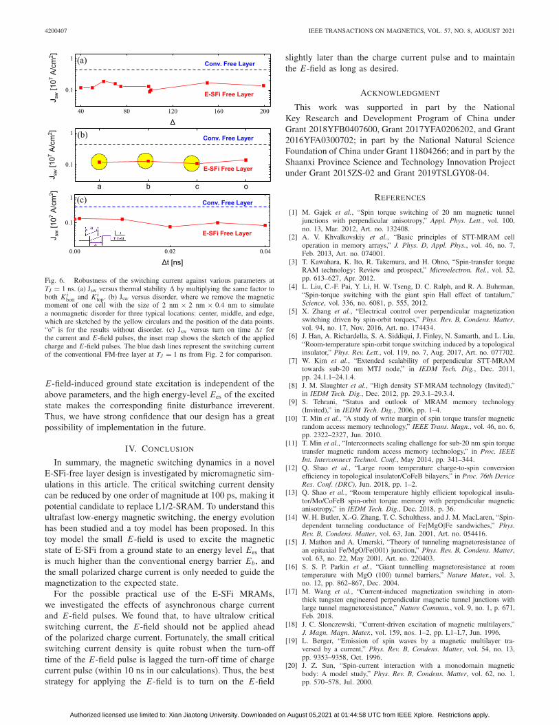
The robustness of the switching in the E-SFi is very impor-tant for practical applications. Thus, we studied its dependenceon various parameters as shown in Fig. 6, with which weconcluded that the switching current of the E-SFi-free layerdesign is quite robust against the thermal stability, disorder,and turn on time of the charge and E-field pulses. Thiscan be also understood by the toy model in Fig. 3, as the
Authorized licensed use limited to: Xian Jiaotong University. Downloaded on August 05,2021 at 01:44:58 UTC from IEEE Xplore. Restrictions apply.
4200407 IEEE TRANSACTIONS ON MAGNETICS, VOL. 57, NO. 8, AUGUST 2021
Fig. 6. Robustness of the switching current against various parameters atTJ = 1 ns. (a) Jsw versus thermal stability by multiplying the same factor toboth K i
bott and K itop. (b) Jsw versus disorder, where we remove the magnetic
moment of one cell with the size of 2 nm × 2 nm × 0.4 nm to simulatea nonmagnetic disorder for three typical locations: center, middle, and edge,which are sketched by the yellow circulars and the position of the data points.“o” is for the results without disorder. (c) Jsw versus turn on time t forthe current and E-field pulses, the inset map shows the sketch of the appliedcharge and E-field pulses. The blue dash lines represent the switching currentof the conventional FM-free layer at TJ = 1 ns from Fig. 2 for comparison.
E-field-induced ground state excitation is independent of theabove parameters, and the high energy-level Ees of the excitedstate makes the corresponding finite disturbance irreverent.Thus, we have strong confidence that our design has a greatpossibility of implementation in the future.
IV. CONCLUSION
In summary, the magnetic switching dynamics in a novelE-SFi-free layer design is investigated by micromagnetic sim-ulations in this article. The critical switching current densitycan be reduced by one order of magnitude at 100 ps, making itpotential candidate to replace L1/2-SRAM. To understand thisultrafast low-energy magnetic switching, the energy evolutionhas been studied and a toy model has been proposed. In thistoy model the small E-field is used to excite the magneticstate of E-SFi from a ground state to an energy level Ees thatis much higher than the conventional energy barrier Eb, andthe small polarized charge current is only needed to guide themagnetization to the expected state.
For the possible practical use of the E-SFi MRAMs,we investigated the effects of asynchronous charge currentand E-field pulses. We found that, to have ultralow criticalswitching current, the E-field should not be applied aheadof the polarized charge current. Fortunately, the small criticalswitching current density is quite robust when the turn-offtime of the E-field pulse is lagged the turn-off time of chargecurrent pulse (within 10 ns in our calculations). Thus, the beststrategy for applying the E-field is to turn on the E-field
slightly later than the charge current pulse and to maintainthe E-field as long as desired.
ACKNOWLEDGMENT
This work was supported in part by the NationalKey Research and Development Program of China underGrant 2018YFB0407600, Grant 2017YFA0206202, and Grant2016YFA0300702; in part by the National Natural ScienceFoundation of China under Grant 11804266; and in part by theShaanxi Province Science and Technology Innovation Projectunder Grant 2015ZS-02 and Grant 2019TSLGY08-04.
REFERENCES
[1] M. Gajek et al., “Spin torque switching of 20 nm magnetic tunneljunctions with perpendicular anisotropy,” Appl. Phys. Lett., vol. 100,no. 13, Mar. 2012, Art. no. 132408.
[2] A. V. Khvalkovskiy et al., “Basic principles of STT-MRAM celloperation in memory arrays,” J. Phys. D, Appl. Phys., vol. 46, no. 7,Feb. 2013, Art. no. 074001.
[3] T. Kawahara, K. Ito, R. Takemura, and H. Ohno, “Spin-transfer torqueRAM technology: Review and prospect,” Microelectron. Rel., vol. 52,pp. 613–627, Apr. 2012.
[4] L. Liu, C.-F. Pai, Y. Li, H. W. Tseng, D. C. Ralph, and R. A. Buhrman,“Spin-torque switching with the giant spin Hall effect of tantalum,”Science, vol. 336, no. 6081, p. 555, 2012.
[5] X. Zhang et al., “Electrical control over perpendicular magnetizationswitching driven by spin-orbit torques,” Phys. Rev. B, Condens. Matter,vol. 94, no. 17, Nov. 2016, Art. no. 174434.
[6] J. Han, A. Richardella, S. A. Siddiqui, J. Finley, N. Samarth, and L. Liu,“Room-temperature spin-orbit torque switching induced by a topologicalinsulator,” Phys. Rev. Lett., vol. 119, no. 7, Aug. 2017, Art. no. 077702.
[7] W. Kim et al., “Extended scalability of perpendicular STT-MRAMtowards sub-20 nm MTJ node,” in IEDM Tech. Dig., Dec. 2011,pp. 24.1.1–24.1.4.
[8] J. M. Slaughter et al., “High density ST-MRAM technology (Invited),”in IEDM Tech. Dig., Dec. 2012, pp. 29.3.1–29.3.4.
[9] S. Tehrani, “Status and outlook of MRAM memory technology(Invited),” in IEDM Tech. Dig., 2006, pp. 1–4.
[10] T. Min et al., “A study of write margin of spin torque transfer magneticrandom access memory technology,” IEEE Trans. Magn., vol. 46, no. 6,pp. 2322–2327, Jun. 2010.
[11] T. Min et al., “Interconnects scaling challenge for sub-20 nm spin torquetransfer magnetic random access memory technology,” in Proc. IEEEInt. Interconnect Technol. Conf., May 2014, pp. 341–344.
[12] Q. Shao et al., “Large room temperature charge-to-spin conversionefficiency in topological insulator/CoFeB bilayers,” in Proc. 76th DeviceRes. Conf. (DRC), Jun. 2018, pp. 1–2.
[13] Q. Shao et al., “Room temperature highly efficient topological insula-tor/Mo/CoFeB spin-orbit torque memory with perpendicular magneticanisotropy,” in IEDM Tech. Dig., Dec. 2018, p. 36.
[14] W. H. Butler, X.-G. Zhang, T. C. Schulthess, and J. M. MacLaren, “Spin-dependent tunneling conductance of Fe|MgO|Fe sandwiches,” Phys.Rev. B, Condens. Matter, vol. 63, Jan. 2001, Art. no. 054416.
[15] J. Mathon and A. Umerski, “Theory of tunneling magnetoresistance ofan epitaxial Fe/MgO/Fe(001) junction,” Phys. Rev. B, Condens. Matter,vol. 63, no. 22, May 2001, Art. no. 220403.
[16] S. S. P. Parkin et al., “Giant tunnelling magnetoresistance at roomtemperature with MgO (100) tunnel barriers,” Nature Mater., vol. 3,no. 12, pp. 862–867, Dec. 2004.
[17] M. Wang et al., “Current-induced magnetization switching in atom-thick tungsten engineered perpendicular magnetic tunnel junctions withlarge tunnel magnetoresistance,” Nature Commun., vol. 9, no. 1, p. 671,Feb. 2018.
[18] J. C. Slonczewski, “Current-driven excitation of magnetic multilayers,”J. Magn. Magn. Mater., vol. 159, nos. 1–2, pp. L1–L7, Jun. 1996.
[19] L. Berger, “Emission of spin waves by a magnetic multilayer tra-versed by a current,” Phys. Rev. B, Condens. Matter, vol. 54, no. 13,pp. 9353–9358, Oct. 1996.
[20] J. Z. Sun, “Spin-current interaction with a monodomain magneticbody: A model study,” Phys. Rev. B, Condens. Matter, vol. 62, no. 1,pp. 570–578, Jul. 2000.
Authorized licensed use limited to: Xian Jiaotong University. Downloaded on August 05,2021 at 01:44:58 UTC from IEEE Xplore. Restrictions apply.
WANG et al.: LOW-ENERGY PICOSECOND MAGNETIC SWITCHING 4200407
[21] Z. Diao et al., “Spin-transfer torque switching in magnetic tunneljunctions and spin-transfer torque random access memory,” J. Phys.,Condens. Matter, vol. 19, no. 16, Apr. 2007, Art. no. 165209.
[22] G. Jan et al., “Achieving sub-ns switching of STT-MRAM for futureembedded LLC applications through improvement of nucleation andpropagation switching mechanisms,” in Proc. IEEE Symp. VLSI Technol.,Jun. 2016, pp. 1–2.
[23] T. Maruyama et al., “Large voltage-induced magnetic anisotropy changein a few atomic layers of iron,” Nature Nanotechnol., vol. 4, no. 3,pp. 158–161, Mar. 2009.
[24] W.-G. Wang, M. Li, S. Hageman, and C. L. Chien, “Electric-field-assisted switching in magnetic tunnel junctions,” Nature Mater., vol. 11,no. 1, pp. 64–68, Jan. 2012.
[25] P. K. Amiri and K. L. Wang, “Voltage-controlled magnetic anisotropyin spintronic devices,” SPIN, vol. 2, no. 3, Sep. 2012, Art. no. 1240002.
[26] W. Kang, Y. Ran, Y. Zhang, W. Lv, and W. Zhao, “Modeling andexploration of the voltage-controlled magnetic anisotropy effect for thenext-generation low-power and high-speed MRAM applications,” IEEETrans. Nanotechnol., vol. 16, no. 3, pp. 387–395, May 2017.
[27] K. L. Wang, H. Lee, and P. K. Amiri, “Magnetoelectric random accessmemory-based circuit design by using voltage-controlled magneticanisotropy in magnetic tunnel junctions,” IEEE Trans. Nanotechnol.,vol. 14, no. 6, pp. 992–997, Nov. 2015.
[28] P. Khalili and K. Wang, “Electric-field-controlled MRAM based onvoltage control of magnetic anisotropy (VCMA): Recent progress andperspectives,” in Proc. 4th Berkeley Symp. Energy Efficient Electron.Syst. (E S), Oct. 2015, p. 1.
[29] T. Nozaki et al., “Highly efficient voltage control of spin and enhancedinterfacial perpendicular magnetic anisotropy in iridium-doped Fe/MgOmagnetic tunnel junctions,” NPG Asia Mater., vol. 9, no. 12, p. e451,Dec. 2017.
[30] M. Yi, H. Zhang, and B.-X. Xu, “Voltage-driven charge-mediated fast180 degree magnetization switching in nanoheterostructure at roomtemperature,” NPJ Comput. Mater., vol. 3, no. 1, p. 38, Sep. 2017.
[31] S. Zhao et al., “Ionic liquid gating control of spin reorientation transi-tion and switching of perpendicular magnetic anisotropy,” Adv. Mater.,vol. 30, no. 30, Jul. 2018, Art. no. 1801639.
[32] U. Bauer, M. Przybylski, and G. S. D. Beach, “Voltage control ofmagnetic anisotropy in Fe films with quantum well states,” Phys.Rev. B, Condens. Matter, vol. 89, May 2014, Art. no. 174402, doi:10.1103/PhysRevB.89.174402.
[33] Q. Yang et al., “Voltage control of perpendicular magnetic anisotropy inmultiferroic (Co/Pt)3/PbMg1/3Nb2/3O3-PbTiO3 heterostructures,” Phys.Rev. A, Gen. Phys., vol. 8, no. 4, Oct. 2017, Art. no. 044006, doi:10.1103/PhysRevApplied.8.044006.
[34] T. Nozaki et al., “Enhancement in the interfacial perpendicular magneticanisotropy and the voltage-controlled magnetic anisotropy by heavymetal doping at the Fe/MgO interface,” APL Mater., vol. 6, no. 2,Feb. 2018, Art. no. 026101.
[35] J. Suwardy, M. Goto, Y. Suzuki, and S. Miwa, “Voltage-controlled mag-netic anisotropy and Dzyaloshinskii–Moriya interactions in CoNi/MgOand CoNi/Pd/MgO,” Jpn. J. Appl. Phys., vol. 58, no. 6, Jun. 2019,Art. no. 060917.
[36] Q. Yang et al., “Ionic liquid gating control of RKKY interaction inFeCoB/Ru/FeCoB and (Pt/Co)2/Ru/(Co/Pt)2 multilayers,” Nature Com-mun., vol. 9, no. 1, p. 991, Mar. 2018.
[37] A. O. Leon, J. d’Albuquerque e Castro, J. C. Retamal, A. B. Cahaya,and D. Altbir, “Manipulation of the RKKY exchange by voltages,” Phys.Rev. B, Condens. Matter, vol. 100, no. 1, Jul. 2019, Art. no. 014403.
[38] M. Fechner, P. Zahn, S. Ostanin, M. Bibes, and I. Mertig, “Switchingmagnetization by 180◦ with an electric field,” Phys. Rev. Lett., vol. 108,May 2012, Art. no. 197206, doi: 10.1103/PhysRevLett.108.197206.
[39] C.-Y. You and S. D. Bader, “Prediction of switching/rotation of themagnetization direction with applied voltage in a controllable interlayerexchange coupled system,” J. Magn. Magn. Mater., vol. 195, no. 2,pp. 488–500, May 1999.
[40] M. A. Ruderman and C. Kittel, “Indirect exchange coupling of nuclearmagnetic moments by conduction electrons,” Phys. Rev., vol. 96, no. 1,pp. 99–102, Oct. 1954.
[41] T. Kasuya, “A theory of metallic ferro- and antiferromagnetism onZener’s model,” Prog. Theor. Phys., vol. 16, no. 1, pp. 45–57, Jul. 1956.
[42] K. Yosida, “Magnetic properties of Cu-Mn alloys,” Phys. Rev., vol. 106,no. 5, pp. 893–898, Jun. 1957.
[43] S. S. P. Parkin and D. Mauri, “Spin engineering: Direct determinationof the Ruderman-Kittel-Kasuya-Yosida far-field range function in ruthe-nium,” Phys. Rev. B, Condens. Matter, vol. 44, no. 13, pp. 7131–7134,Oct. 1991.
[44] R. Hao, L. Wang, and T. Min, “A novel STT-MRAM design withelectric-field-assisted synthetic anti-ferromagnetic free layer,” IEEETrans. Magn., vol. 55, no. 3, pp. 1–6, Mar. 2019.
[45] M. J. Donahue and D. G. Porter, “OOMMF user’s guide, version 1.0,”Nat. Inst. Standards Technol., Gaithersburg, MD, USA, Tech. Rep.NISTIR 6376, 1999.
[46] A. V. Khvalkovskiy et al., “High domain wall velocities due to spincurrents perpendicular to the plane,” Phys. Rev. Lett., vol. 102, no. 6,Feb. 2009, Art. no. 067206.
[47] T. L. Gilbert, “A Lagrangian formulation of the gyromagnetic equationof the magnetization field,” Phys. Rev., vol. 100, p. 1243, Jan. 1955.
[48] L. D. Landau and E. Lifshitz, “On the theory of the dispersion ofmagnetic permeability in ferromagnetic bodies,” Phys. Zeitsch. Sow.,vol. 8, p. 153, Jun. 1935.
[49] J. Xiao, A. Zangwill, and M. D. Stiles, “Boltzmann test of Slonczewski’stheory of spin-transfer torque,” Phys. Rev. B, Condens. Matter, vol. 70,Nov. 2004, Art. no. 172405.
[50] X. Liu, W. Zhang, M. J. Carter, and G. Xiao, “Ferromagnetic resonanceand damping properties of CoFeB thin films as free layers in MgO-basedmagnetic tunnel junctions,” J. Appl. Phys., vol. 110, no. 3, Aug. 2011,Art. no. 033910.
[51] T. Devolder et al., “Damping of Cox Fe80−x B20 ultrathin films withperpendicular magnetic anisotropy,” Appl. Phys. Lett., vol. 102, no. 2,Jan. 2013, Art. no. 022407.
[52] S. Ikeda et al., “A perpendicular-anisotropy CoFeB-MgO magnetictunnel junction,” Nature Mater., vol. 9, no. 9, pp. 721–724, Jul. 2010.
[53] S.-C. Oh et al., “Bias-voltage dependence of perpendicular spin transfertorque in asymmetric MgO-based magnetic tunnel junctions,” in Proc.APS Meeting Abstr., Mar. 2010, Art. no. L37.010. [Online]. Available:http://www.meetings.aps.org/Meeting/MAR10/Event/119978
[54] J. C. Sankey, Y.-T. Cui, J. Z. Sun, J. C. Slonczewski, R. A. Buhrman,and D. C. Ralph, “Measurement of the spin-transfer-torque vector inmagnetic tunnel junctions,” Nature Phys., vol. 4, no. 1, pp. 67–71,Jan. 2008.
[55] H. Kubota et al., “Quantitative measurement of voltage dependence ofspin-transfer torque in MgO-based magnetic tunnel junctions,” NaturePhys., vol. 4, no. 1, pp. 37–41, Jan. 2008.
[56] A. M. Deac et al., “Bias-driven high-power microwave emission fromMgO-based tunnel magnetoresistance devices,” Nature Phys., vol. 4,no. 10, pp. 803–809, Oct. 2008.
[57] D. V. Berkov, C. T. Boone, and I. N. Krivorotov, “Micromagneticsimulations of magnetization dynamics in a nanowire induced by a spin-polarized current injected via a point contact,” Phys. Rev. B, Condens.Matter, vol. 83, Feb. 2011, Art. no. 054420.
[58] M. Wyss et al., “Imaging magnetic vortex configurations in ferro-magnetic nanotubes,” Phys. Rev. B, Condens. Matter, vol. 96, no. 2,Jul. 2017, Art. no. 024423, doi: 10.1103/PhysRevB.96.024423.
[59] A. van den Brink et al., “Spin-Hall-assisted magnetic random accessmemory,” Appl. Phys. Lett., vol. 104, no. 1, Jan. 2014, Art. no. 012403.
[60] S. Ikeda et al., “Magnetic tunnel junctions for spintronic memories andbeyond,” IEEE Trans. Electron Devices, vol. 54, no. 5, pp. 991–1002,May 2007.
[61] R. Heindl, A. Chaudhry, and S. E. Russek, “Estimation of thermal stabil-ity factor and intrinsic switching current from switching distributions inspin-transfer-torque devices with out-of-plane magnetic anisotropy,” AIPAdv., vol. 8, no. 1, Jan. 2018, Art. no. 015011, doi: 10.1063/1.5002139.
[62] S. Bhatti, R. Sbiaa, A. Hirohata, H. Ohno, S. Fukami, andS. N. Piramanayagam, “Spintronics based random access memory:A review,” Mater. Today, vol. 20, no. 9, pp. 530–548, Nov. 2017.
[63] S. Peng et al., “Interfacial perpendicular magnetic anisotropy in sub-20 nm tunnel junctions for large-capacity spin-transfer torque magneticrandom-access memory,” IEEE Magn. Lett., vol. 8, pp. 1–5, 2017.
[64] N. Bukar, S. S. Zhao, D. M. Charbonneau, J. N. Pelletier, andJ.-F. Masson, “Influence of the Debye length on the interaction of asmall molecule-modified Au nanoparticle with a surface-bound biore-ceptor,” Chem. Commun., vol. 50, pp. 4947–4950, 2014.
[65] J. J. Kan et al., “Systematic validation of 2x nm diameter perpendicularMTJ arrays and MgO barrier for sub-10 nm embedded STT-MRAMwith practically unlimited endurance,” in IEDM Tech. Dig., Dec. 2016,p. 27.
[66] C. Park et al., “Low RA magnetic tunnel junction arrays in conjunctionwith low switching current and high breakdown voltage for STT-MRAMat 10 nm and beyond,” in Proc. IEEE Symp. VLSI Technol., Jun. 2018,pp. 185–186.
[67] G. Jan et al., “Demonstration of ultra-low voltage and ultra low powerSTT-MRAM designed for compatibility with 0x node embedded LLCapplications,” in Proc. IEEE Symp. VLSI Technol., Jun. 2018, pp. 65–66.
Authorized licensed use limited to: Xian Jiaotong University. Downloaded on August 05,2021 at 01:44:58 UTC from IEEE Xplore. Restrictions apply.