LAN LI,1 SPENCER NOVAK,4,5 KATHLEEN RICHARDSON,4 WEI ZHANG,1,6 AND JUEJUN HU1,*1Department of Materials Science and Engineering, Massachusetts Institute of Technology, Cambridge, Massachusetts 02139, USA2Department of Electronic Engineering, Xiamen University, Xiamen 361005, China3The Key Laboratory of Optoelectronic Technology & Systems, Education Ministry of China, Chongqing University, Chongqing 400044, China4College of Optics and Photonics, CREOL, Department of Materials Science and Engineering, University of Central Florida, Orlando,Florida 32816, USA5Currently at Lightpath Technologies, Orlando, Florida 32816, USA6Key Laboratory of Photoelectric Materials and Devices of Zhejiang Province, Ningbo University, Ningbo, Zhejiang 315211, China*Corresponding author: [email protected]
Received 29 April 2016; revised 7 June 2016; accepted 7 June 2016; posted 7 June 2016 (Doc. ID 263870); published 29 June 2016
Chalcogenide glasses (ChGs) are widely recognized as thematerial of choice for sensing, flexible substrate integration,and all-optical signal processing due to their broad transparencywindow in the infrared region, low processing temperature, andhigh Kerr nonlinearity [1–5]. In addition, their high refractiveindices enable small optical mode volume without sufferingfrom excessive radiative loss. Nevertheless, unlike standard in-tegrated photonic materials with well-established processingprotocols such as silicon and silica, planar processing of ChGsremains much less mature despite their exceptional opticalproperties. Prior work has explored planar ChG photonic de-vice fabrication using standard semiconductor microfabricationtechniques such as plasma etching, wet etching [6], ion milling[7], nanoimprint [8,9], and lift-off [10]. In particular, Maddenet al. [11] demonstrated a remarkable low propagation loss of0.05 dB/cm in large-core rib waveguides via fluorine plasmaetching. Small-core single-mode strip waveguides, however, suf-fer from much higher loss due to the stronger optical modal
overlap with rough waveguide sidewalls. The best reported re-sult of 0.84 dB/cm was obtained recently by Chiles et al. [12]using plasma etching with a chlorine chemistry. We note thatin both cases, the waveguide loss figures far exceed theintrinsic material attenuation in ChG materials, as quality fac-tors (Q-factors) as high as 7.2 × 10⁷, which corresponds to anoptical loss of less than 0.002 dB/cm, have been reported inChG microspheres [13]. It is apparent that optical scatteringfrom waveguide sidewall roughness and possibly glass inhomo-geneity [14] represents the dominant attenuation mechanismin the measured waveguide loss.
Our prior work had relied on UV photolithography forChG microphotonic device fabrication, although large sidewallroughness (10–5 nm rms [15]) due to the limited feature res-olution can compromise the resulting device performance. Inthis Letter, we report a systematic study of low-loss ChG deviceprocessing using electron beam (e-beam) lithography coupledwith reactive ion dry etching. Compared to UV photolithogra-phy, e-beam lithography is known to offer deep-submicrometerresolution and significantly reduced pattern edge roughness, andis therefore suited for low-loss, high-index-contrast ChG deviceprocessing. Both chlorine and fluorine etching gases are investi-gated, as both chemistries have been adopted for low-loss ChGdevice patterning [11,12].
The ChG devices were fabricated on 6 in. (153 mm) siliconwafers with 3 μm thermally grown oxide coating (Silicon QuestInternational). A piranha clean was performed prior to filmdeposition to remove any organic residue from the wafer sur-face. Subsequently, Ge23Sb7S70 (GSS) bulk glass prepared byconventional melt/quench protocols previously reported [16]was thermally evaporated onto the wafer to form a 450-nm-thick ChG film using established protocols [16]. We chose theGSS composition over the classical As2S3 or As2Se3 systemsgiven the superior oxidation resistance of GSS glass, whereasAs2S3 or As2Se3 glasses are prone to surface oxidation [9]. Thedeposition rate was maintained at 15 Å/s. A 400-nm-thickZEP-520A resist (ZEON Chemicals) layer was then spun onto
3090 Vol. 41, No. 13 / July 1 2016 / Optics Letters Letter
the glass film and exposed by an Elionix ELS-F125 e-beamlithography tool using a beam current of 10 nA. The resistwas then developed by immersing in ZED-N50 (ZEONChemicals) for 1 min to reveal the patterns.
Reactive ion etching (RIE) was then carried out on aPlasmaTherm RIE tool (PlasmaTherm Inc.). Both chlorine andfluorine chemistries were investigated. In both cases, the gasflow rate, chamber pressure, radio-frequency (RF) power, andetching gas ratio (for the fluorine chemistry) were systematicallyvaried to determine the optimal etching recipes that generatephotonic devices with minimal loss (detailed results notshown). Table 1 summarizes the optimized etching parametersfor both chemistries. Channel waveguides with cross-sectionaldimensions of 800 nm × 450 nm were fabricated by etchingthrough the entire GSS layer. After etching, remainingresists were stripped by soaking the sample in N-methyl-2-pyrrolidone (NMP) for 2 h and then sonicating for 30 s.The fluorine etched samples underwent an additional oxygenplasma treatment step to remove the fluorocarbon polymerdeposited on the waveguide sidewalls formed during theplasma process.
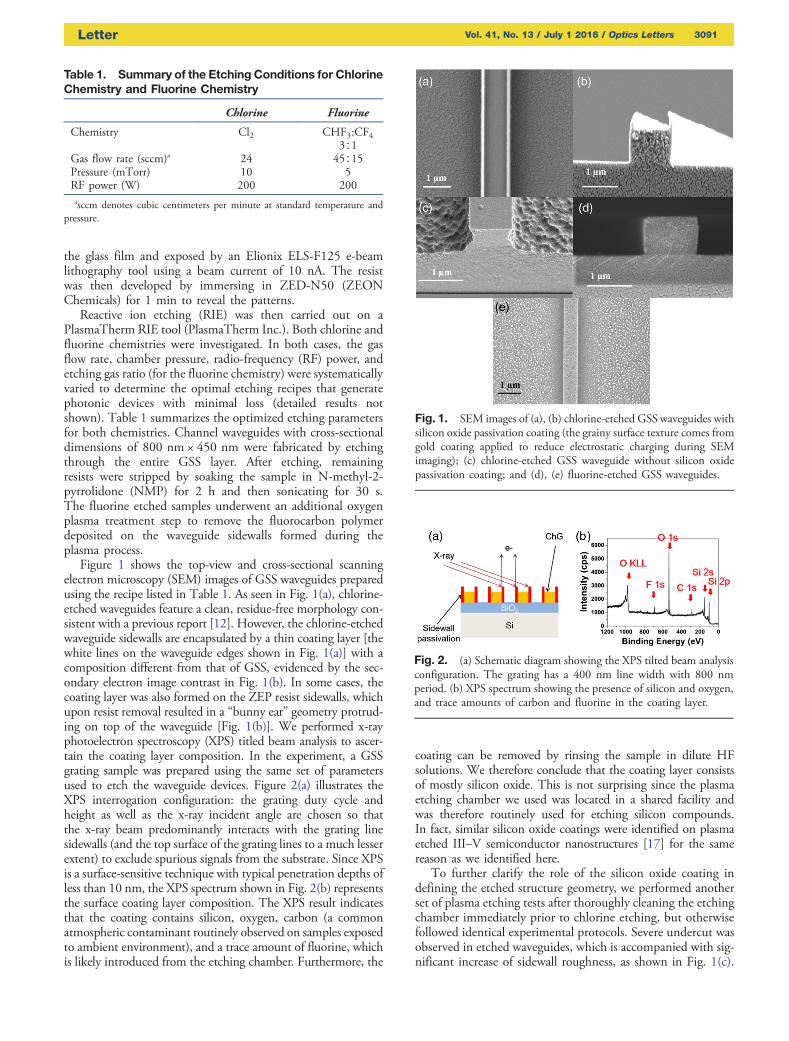
Figure 1 shows the top-view and cross-sectional scanningelectron microscopy (SEM) images of GSS waveguides preparedusing the recipe listed in Table 1. As seen in Fig. 1(a), chlorine-etched waveguides feature a clean, residue-free morphology con-sistent with a previous report [12]. However, the chlorine-etchedwaveguide sidewalls are encapsulated by a thin coating layer [thewhite lines on the waveguide edges shown in Fig. 1(a)] with acomposition different from that of GSS, evidenced by the sec-ondary electron image contrast in Fig. 1(b). In some cases, thecoating layer was also formed on the ZEP resist sidewalls, whichupon resist removal resulted in a “bunny ear” geometry protrud-ing on top of the waveguide [Fig. 1(b)]. We performed x-rayphotoelectron spectroscopy (XPS) titled beam analysis to ascer-tain the coating layer composition. In the experiment, a GSSgrating sample was prepared using the same set of parametersused to etch the waveguide devices. Figure 2(a) illustrates theXPS interrogation configuration: the grating duty cycle andheight as well as the x-ray incident angle are chosen so thatthe x-ray beam predominantly interacts with the grating linesidewalls (and the top surface of the grating lines to a much lesserextent) to exclude spurious signals from the substrate. Since XPSis a surface-sensitive technique with typical penetration depths ofless than 10 nm, the XPS spectrum shown in Fig. 2(b) representsthe surface coating layer composition. The XPS result indicatesthat the coating contains silicon, oxygen, carbon (a commonatmospheric contaminant routinely observed on samples exposedto ambient environment), and a trace amount of fluorine, whichis likely introduced from the etching chamber. Furthermore, the
coating can be removed by rinsing the sample in dilute HFsolutions. We therefore conclude that the coating layer consistsof mostly silicon oxide. This is not surprising since the plasmaetching chamber we used was located in a shared facility andwas therefore routinely used for etching silicon compounds.In fact, similar silicon oxide coatings were identified on plasmaetched III–V semiconductor nanostructures [17] for the samereason as we identified here.
To further clarify the role of the silicon oxide coating indefining the etched structure geometry, we performed anotherset of plasma etching tests after thoroughly cleaning the etchingchamber immediately prior to chlorine etching, but otherwisefollowed identical experimental protocols. Severe undercut wasobserved in etched waveguides, which is accompanied with sig-nificant increase of sidewall roughness, as shown in Fig. 1(c).
Fig. 1. SEM images of (a), (b) chlorine-etched GSS waveguides withsilicon oxide passivation coating (the grainy surface texture comes fromgold coating applied to reduce electrostatic charging during SEMimaging); (c) chlorine-etched GSS waveguide without silicon oxidepassivation coating; and (d), (e) fluorine-etched GSS waveguides.
Fig. 2. (a) Schematic diagram showing the XPS tilted beam analysisconfiguration. The grating has a 400 nm line width with 800 nmperiod. (b) XPS spectrum showing the presence of silicon and oxygen,and trace amounts of carbon and fluorine in the coating layer.
Table 1. Summary of the Etching Conditions for ChlorineChemistry and Fluorine Chemistry
Chlorine Fluorine
Chemistry Cl2 CHF3:CF43∶1
Gas flow rate (sccm)a 24 45∶15Pressure (mTorr) 10 5RF power (W) 200 200asccm denotes cubic centimeters per minute at standard temperature and
pressure.
Letter Vol. 41, No. 13 / July 1 2016 / Optics Letters 3091
The result suggests that the silicon oxide coating that sponta-neously forms during the plasma etching step is essential tominimizing radical chemical attack on the GSS pattern side-walls and maintaining a vertical sidewall profile. This can beenvisioned, as silicon oxide is known to be inert in a chlorineplasma.
Figures 1(d) and 1(e) show that fluorine etching similarlygenerates a nearly vertical sidewall profile. During the fluorineetch, carbon and fluorine radicals generated by the plasma reactto form a fluorocarbon polymer passivation layer on the side-wall that prevents lateral etching. The fluorocarbon polymercoating also accounts for the residue observed on the etchedsurfaces at the two sides of the waveguide [Fig. 1(d)] formedby self-masking [18]. It is interesting to note that the vicinity ofthe waveguide is free of residues, likely due to shadowing effect.This phenomenon is useful to producing waveguide deviceswith smooth sidewalls and low optical loss.
Performance of the fabricated devices near 1550 nm wave-length was evaluated using a fiber end fire coupling methodon a LUNATechnology laser with a built-in optical vector ana-lyzer. To quantitatively assess propagation loss, microring andmicrodisk resonators were fabricated by both chlorine and fluo-rine etching. Optical micrographs of the fabricated resonatorsamples are shown in Figs. 3(a) and 3(b). All resonators are50 μm in radius. Both the microring and the coupling bus wave-guides have cross-sectional dimensions of 800 nm × 450 nm.Figure 3(c) plots a representative transmission spectrum ofthe microring resonator. The best microring resonator perfor-mance is obtained in devices etched by the fluorine chemistry,which yields an intrinsic Q-factor of 750,000. The waveguidepropagation loss α (in cm−1) is calculated by
α � 2πngQλr
; (1)
where λr denotes the resonant wavelength, and ng represents thegroup index. The group index is inferred from the free spectralrange (FSR),
ng �λ2r
L × FSR; (2)
and found to be 2.30. Here, L is the round-trip length of theresonator. Equation (1) gives a waveguide propagation loss of0.5 dB/cm. To the best of our knowledge, this value representsthe lowest loss figure reported in submicrometer single-modeChG channel waveguides.
Microdisk resonators prepared using the same etching pro-tocols yield high Q-factors of 106 (not shown) for chlorineetched samples and 1.2 × 10⁶ [Fig. 3(f )] for fluorine etchedsamples, the highest Q-factors so far reported in planar ChGoptical devices [12,19–23]. Although both etching chemistriesare capable of producing highQ-factors, fluorine etching is pre-ferred over chlorine etching in our case, since sidewall passiva-tion using silicon oxide in the case of chlorine etching requiresdeliberate introduction of trace silica contaminants into theetching chamber, which is far less reproducible compared tofluorocarbon polymer formation during fluorine etching.
To quantify the roughness scattering contribution to opticalloss, sidewall roughness of the waveguides was determined fromhigh-magnification SEM images using the imaging processingsoftware ImageJ. In the example shown in Fig. 4, the waveguideedge profile, represented by a function f �z�, was extracted
from the image using gray-scale analysis. The roughness metricswere subsequently evaluated following procedures describedin Ref. [24], and the results were averaged over multiple wave-guides. Specifically, the autocorrelation function of the wave-guide sidewall roughness is calculated using
R�u� � hf �z� · f �z � u�i; (3)
where the brackets represent ensemble average. The roughnesspower spectral density (PSD) function is the Fourier transformof R�u�. The PSD function is plotted in Fig. 4(c), and a rmsroughness of �2.4� 0.2� nm for fluorine etched waveguides isobtained from the analysis. Figure 4(c) further suggests that theroughness distribution does not comply with either the expo-nential model or the white noise model. Following the 3Dvolume current method in Ref. [24], we estimate that sidewall
Fig. 3. Optical microscope images of fabricated (a) microdisk and(b) microring resonators. Transmission spectra of (c) microring reso-nator and (d) microdisk resonator etched using the fluorine chemistry.The red curves are Lorentzian fits of the spectra.
3092 Vol. 41, No. 13 / July 1 2016 / Optics Letters Letter
roughness scattering contributes approximately 0.2 dB/cmoptical loss.
In summary, we have demonstrated low-loss GSS photonicdevice fabrication using e-beam lithography and plasma etch-ing. Optimized chlorine and fluorine etching chemistries areboth capable of producing vertical sidewalls and low-lossdevices. For fluorine etching, fluorocarbon polymers developduring deposition and provide sidewall passivation, whereasnon-intentionally introduced silicon oxide impurities are theprimary passivation agent in chlorine etching. A low propaga-tion loss of 0.5 dB/cm and a high Q-factor of 1.2 million wereobtained in submicrometer single-mode waveguides and micro-disk resonators patterned using fluorine etching, respectively.These values represent the best low-loss performance reportedto date in planar chalcogenide glass devices.
Funding. Defense Threat Reduction Agency (DTRA)(HDTRA1-13-1-0001); National Science Foundation (NSF)(1453218, 1506605); National Nuclear Security Administration(NNSA) (DE-NA0002509).
Acknowledgment. The authors acknowledge materialcharacterization and fabrication facility support by the MIT
Center of Materials Science & Engineering (CMSE) and theMicrosystems Technology Laboratories.
REFERENCES
1. B. J. Eggleton, B. Luther-Davies, and K. Richardson, Nat. Photonics 5,141 (2011).
2. V. Singh, P. T. Lin, N. Patel, H. Lin, L. Li, Y. Zou, F. Deng, C. Ni, J. Hu,and J. Giammarco, Sci. Technol. Adv. Mater. 15, 014603 (2014).
3. J. Hu, L. Li, H. Lin, Y. Zou, Q. Du, C. Smith, S. Novak, K. Richardson,and J. D. Musgraves, Am. Ceram. Soc. Bull. 94, 24 (2015).
4. L. Li, H. Lin, S. Qiao, Y. Zou, S. Danto, K. Richardson, J. D.Musgraves, N. Lu, and J. Hu, Nat. Photonics 8, 643 (2014).
5. M.-L. Anne, J. Keirsse, V. Nazabal, K. Hyodo, S. Inoue, C. Boussard-Pledel, H. Lhermite, J. Charrier, K. Yanakata, and O. Loreal, Sensors9, 7398 (2009).
6. T. V. Galstyan, J. Viens, A. Villeneuve, K. Richardson, and M.Duguay, J. Lightwave Technol. 15, 1343 (1997).
7. Y. Ruan, W. Li, R. Jarvis, N. Madsen, A. Rode, and B. Luther-Davies,Opt. Express 12, 5140 (2004).
8. T. Han, S. Madden, D. Bulla, and B. Luther-Davies, Opt. Express 18,19286 (2010).
9. Y. Zou, L. Moreel, L. Savelli, H. Lin, J. Zhou, L. Li, S. Danto, J. D.Musgraves, K. Richardson, K. Dobson, R. Birkmire, and J. Hu, Adv.Opt. Mater. 2, 759 (2014).
10. J. Hu, N.-N. Feng, N. Carlie, L. Petit, J. Wang, A. Agarwal, K.Richardson, and L. Kimerling, Opt. Express 15, 14566 (2007).
11. S. Madden, D.-Y. Choi, D. Bulla, A. V. Rode, B. Luther-Davies, V. G.Ta’eed, M. Pelusi, and B. J. Eggleton, Opt. Express 15, 14414 (2007).
12. J. Chiles, M. Malinowski, A. Rao, S. Novak, K. Richardson, and S.Fathpour, Appl. Phys. Lett. 106, 111110 (2015).
13. F. Vanier, M. Rochette, N. Godbout, and Y.-A. Peter, Opt. Lett. 38,4966 (2013).
14. R. Wang, A. V. Rode, S. Madden, C. Zha, R. Jarvis, andB. Luther-Davies, J. Non-Cryst. Solids. 353, 950 (2007).
15. J. Hu, N.-N. Feng, N. Carlie, L. Petit, A. Agarwal, K. Richardson, andL. Kimerling, Opt. Express 18, 1469 (2010).
16. J. Hu, V. Tarasov, A. Agarwal, L. Kimerling, N. Carlie, L. Petit, and K.Richardson, Opt. Express 15, 2307 (2007).
17. S. Bouchoule, R. Chanson, A. Pageau, E. Cambril, S. Guilet, A.Rhallabi, and C. Cardinaud, J. Vac. Sci. Technol. A 33, 05E124(2015).
18. D.-Y. Choi, S. Maden, A. Rode, R. Wang, and B. Luther-Davies,J. Non-Cryst. Solids 354, 3179 (2008).
19. S. Levy, M. Klebanov, and A. Zadok, Photon. Res. 3, 63 (2015).20. X. Gai, B. Luther-Davies, and T. P. White, Opt. Express 20, 15503
(2012).21. P. Ma, D.-Y. Choi, Y. Yu, Z. Yang, K. Vu, T. Nguyen, A. Mitchell, B.
Luther-Davies, and S. Madden, Opt. Express 23, 19969 (2015).22. Y. Zou, D. Zhang, H. Lin, L. Li, L. Moreel, J. Zhou, Q. Du, O. Ogbuu, S.
Danto, J. D. Musgraves, K. Richardson, K. Dobson, R. Birkmire, andJ. Hu, Adv. Opt. Mater. 2, 478 (2014).
23. H. Lin, L. Li, Y. Zou, S. Danto, J. D. Musgraves, K. Richardson, S.Kozacik, M. Murakowski, D. Prather, P. Lin, V. Singh, A. Agarwal,L. C. Kimerling, and J. Hu, Opt. Lett. 38, 1470 (2013).
24. T. Barwicz and H. A. Haus, J. Lightwave Technol. 23, 2719 (2005).
Fig. 4. Waveguide sidewall roughness analysis example. (a) SEMtop-view image of a fluorine etched waveguide; the grainy surface tex-ture comes from gold coating applied to reduce electrostatic chargingduring SEM imaging. (b) Waveguide edge extracted from the SEMimage. (c) PSD function of sidewall roughness (black line). Thered line represents exponential model fit.
Letter Vol. 41, No. 13 / July 1 2016 / Optics Letters 3093