2 ECTI TRANSACTIONS ON COMPUTER AND INFORMATION TECHNOLOGY VOL.2, NO.1 MAY 2006 Low Power Despreader using Dynamic Reconfigurable Architecture for Multicarrier CDMA with Two-Dimensional Spreading and Variable Spreading Factor Takayuki Sugawara 1 and Yoshikazu Miyanaga 2 , Non-members ABSTRACT In this paper, we propose a dynamic reconfigurable architecture of a despreader for Multicarrier code di- vision multiple access (CDMA) with two-dimensional spreading and variable spreading factor. The spread- ing factors in the time and frequency domains are varied according to cell configuration, channel load, and propagation channel conditions in the system. The structure of the proposed despreader is dynami- cally changed with spreading factors. Following this structure, optimum parallel and pipeline processing are achieved. The proposed despreader reduces the power consumption by 60% compared with the basic one. Keywords: low power circuit, dynamic reconfigura- tion, despreader, Multicarrier CDMA 1. INTRODUCTION Recently, there are various researches of the next generation mobile communications (4G) to estab- lish broadband packet transmission with a maximum data rate exceeding 100Mbit/s [1]-[4]. In 4G system, the seamless deployment of wireless access employ- ing one air interface is required in both multi-cell and isolated-cell environments. Multicarrier CDMA, which is examined to be used in 4G system, is based on a combination of orthogonal frequency division multiplexing (OFDM) signaling and CDMA tech- nique. The Multicarrier CDMA schemes are mainly cat- egorized into three groups. The first group spreads the original data in the frequency domain [5],[6]. The second group spreads the original data in the time do- main [7]. The third group spreads the original data in both the frequency and time domains [8]. In ad- dition, the Multicarrier CDMA with variable spread- ing factor, which changes the spreading factor cor- Manuscript received on May 15, 2006. 1 The author is with the Graduate School of Engi- neering, Hokkaido University, Kita 13 Nishi 8, Kita- ku, Sapporo-shi, Hokkaido, 060–8628 Japan; E-mail: [email protected]2 The author is with the Graduate School of Information Science and Technology, Hokkaido University, Kita 14 Nishi 9, Kita-ku, Sapporo-shi, Hokkaido, 060–0814 Japan; E-mail: [email protected]responding to the cell structure, channel load, radio link conditions and radio link parameters, has been proposed [9]. Although several communication meth- ods of the Multicarrier CDMA with two-dimensional spreading and variable spreading factor have been ex- amined [10]-[12], its hardware design has hardly been discussed. However, it is important to design a small size and a low power consumption circuit when the Multicarrier CDMA is mounted on the mobile termi- nal such as the cellular phone. In the Multicarrier CDMA with two-dimensional spreading and variable spreading factor, the module structure that is quit different from a conventional system is a despreader since both spreading factors in the frequency and time domains are changed adap- tively. Although the matched filter is usually used for despreading in the direct sequence CDMA [13], we consider that the sliding correlator can process it in the Multicarrier CDMA. In this paper, the sliding correlator is modified for the two-dimensional spread- ing. Furthermore, the despreader is designed with low power consumption using parallel and pipeline architecture. We have already proposed a dynamic reconfigurable despreader that changes the structure according to the spreading factor [14]. The pro- posed despreader in [14] can achieve parallelization and pipelining. This paper explains a circuit struc- ture of the proposed despreader, and evaluates the area and the power consumption of the designed cir- cuit. 2. MULTICARRIER CDMA WITH TWO- DIMENSIONAL SPREADING AND VARI- ABLE SPREADING FACTOR In the Multicarrier CDMA with two-dimensional spreading and variable spreading factor, the spread- ing factors in the time and frequency domains, i.e. SF t and SF f , are varied according the cell struc- ture in order to achieve higher link capacity in both multi-cell and isolated-cell environments. The config- uration of the two-dimensional spreading is shown in Fig.1. One data symbol is spreaded into SF t succes- sive OFDM-symbols and SF f successive sub-carriers. A total spreading factor SF is SF f × SF t . Fig.2 shows the baseband processing of the receiver for despreading. The symbol timing is detected and
Transcript
2 ECTI TRANSACTIONS ON COMPUTER AND INFORMATION TECHNOLOGY VOL.2, NO.1 MAY 2006
Low Power Despreader using DynamicReconfigurable Architecture for MulticarrierCDMA with Two-Dimensional Spreading and
Variable Spreading Factor
Takayuki Sugawara1 and Yoshikazu Miyanaga2, Non-members
ABSTRACT
In this paper, we propose a dynamic reconfigurablearchitecture of a despreader for Multicarrier code di-vision multiple access (CDMA) with two-dimensionalspreading and variable spreading factor. The spread-ing factors in the time and frequency domains arevaried according to cell configuration, channel load,and propagation channel conditions in the system.The structure of the proposed despreader is dynami-cally changed with spreading factors. Following thisstructure, optimum parallel and pipeline processingare achieved. The proposed despreader reduces thepower consumption by 60% compared with the basicone.
Keywords: low power circuit, dynamic reconfigura-tion, despreader, Multicarrier CDMA
1. INTRODUCTION
Recently, there are various researches of the nextgeneration mobile communications (4G) to estab-lish broadband packet transmission with a maximumdata rate exceeding 100Mbit/s [1]-[4]. In 4G system,the seamless deployment of wireless access employ-ing one air interface is required in both multi-celland isolated-cell environments. Multicarrier CDMA,which is examined to be used in 4G system, is basedon a combination of orthogonal frequency divisionmultiplexing (OFDM) signaling and CDMA tech-nique.
The Multicarrier CDMA schemes are mainly cat-egorized into three groups. The first group spreadsthe original data in the frequency domain [5],[6]. Thesecond group spreads the original data in the time do-main [7]. The third group spreads the original datain both the frequency and time domains [8]. In ad-dition, the Multicarrier CDMA with variable spread-ing factor, which changes the spreading factor cor-
Manuscript received on May 15, 2006.1The author is with the Graduate School of Engi-
2The author is with the Graduate School of InformationScience and Technology, Hokkaido University, Kita 14 Nishi9, Kita-ku, Sapporo-shi, Hokkaido, 060–0814 Japan; E-mail:[email protected]
responding to the cell structure, channel load, radiolink conditions and radio link parameters, has beenproposed [9]. Although several communication meth-ods of the Multicarrier CDMA with two-dimensionalspreading and variable spreading factor have been ex-amined [10]-[12], its hardware design has hardly beendiscussed. However, it is important to design a smallsize and a low power consumption circuit when theMulticarrier CDMA is mounted on the mobile termi-nal such as the cellular phone.
In the Multicarrier CDMA with two-dimensionalspreading and variable spreading factor, the modulestructure that is quit different from a conventionalsystem is a despreader since both spreading factorsin the frequency and time domains are changed adap-tively. Although the matched filter is usually usedfor despreading in the direct sequence CDMA [13],we consider that the sliding correlator can process itin the Multicarrier CDMA. In this paper, the slidingcorrelator is modified for the two-dimensional spread-ing. Furthermore, the despreader is designed withlow power consumption using parallel and pipelinearchitecture. We have already proposed a dynamicreconfigurable despreader that changes the structureaccording to the spreading factor [14]. The pro-posed despreader in [14] can achieve parallelizationand pipelining. This paper explains a circuit struc-ture of the proposed despreader, and evaluates thearea and the power consumption of the designed cir-cuit.
2. MULTICARRIER CDMA WITH TWO-DIMENSIONAL SPREADING AND VARI-ABLE SPREADING FACTOR
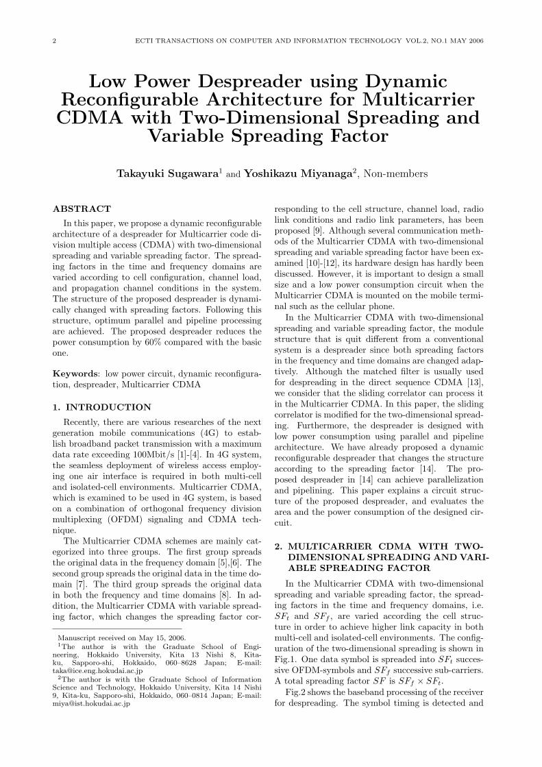
In the Multicarrier CDMA with two-dimensionalspreading and variable spreading factor, the spread-ing factors in the time and frequency domains, i.e.SFt and SFf , are varied according the cell struc-ture in order to achieve higher link capacity in bothmulti-cell and isolated-cell environments. The config-uration of the two-dimensional spreading is shown inFig.1. One data symbol is spreaded into SFt succes-sive OFDM-symbols and SFf successive sub-carriers.A total spreading factor SF is SFf × SFt.
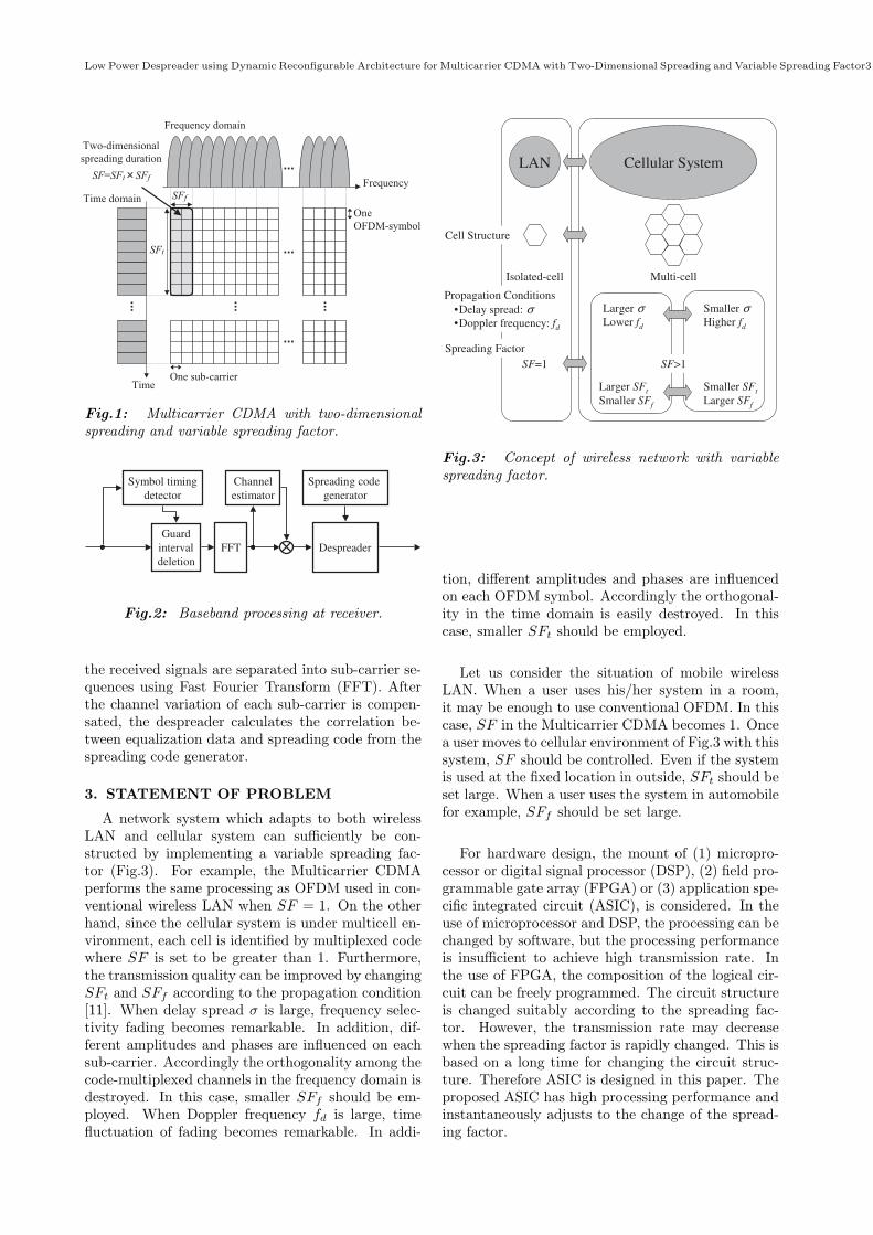
Fig.2 shows the baseband processing of the receiverfor despreading. The symbol timing is detected and
Low Power Despreader using Dynamic Reconfigurable Architecture for Multicarrier CDMA with Two-Dimensional Spreading and Variable Spreading Factor3
SFf
SFt
One
OFDM-symbol
One sub-carrier
Frequency
Time
Frequency domain
Time domain
Two-dimensional
spreading duration
SF=SFt SFf
Fig.1: Multicarrier CDMA with two-dimensionalspreading and variable spreading factor.
Guardintervaldeletion
Symbol timingdetector
Channelestimator
Spreading codegenerator
FFT Despreader
Fig.2: Baseband processing at receiver.
the received signals are separated into sub-carrier se-quences using Fast Fourier Transform (FFT). Afterthe channel variation of each sub-carrier is compen-sated, the despreader calculates the correlation be-tween equalization data and spreading code from thespreading code generator.
3. STATEMENT OF PROBLEM
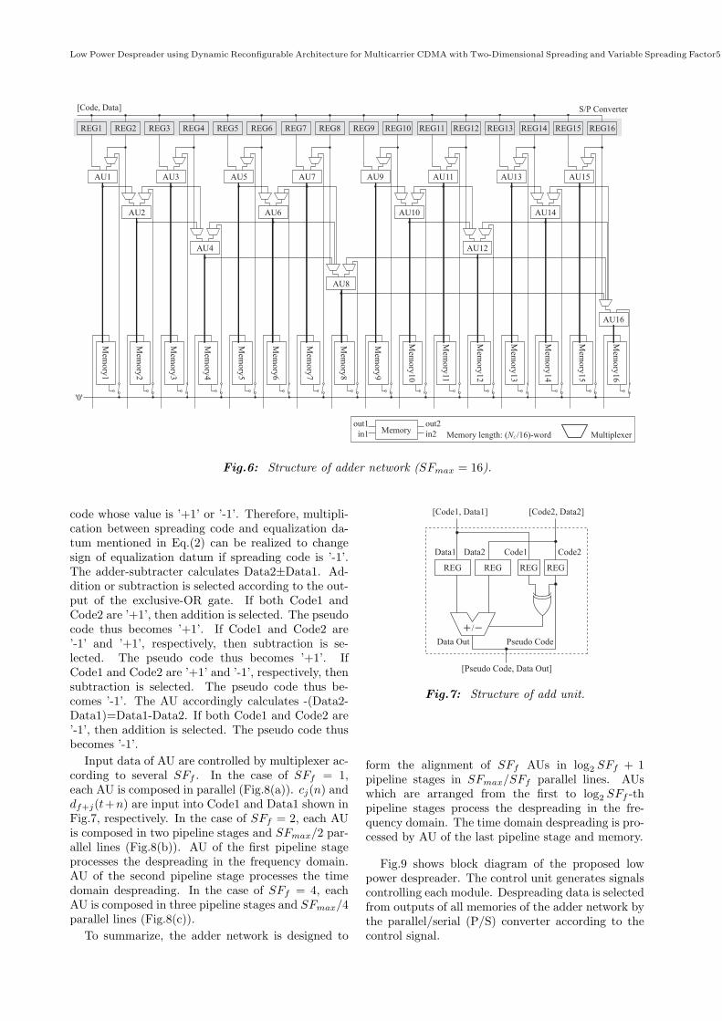
A network system which adapts to both wirelessLAN and cellular system can sufficiently be con-structed by implementing a variable spreading fac-tor (Fig.3). For example, the Multicarrier CDMAperforms the same processing as OFDM used in con-ventional wireless LAN when SF = 1. On the otherhand, since the cellular system is under multicell en-vironment, each cell is identified by multiplexed codewhere SF is set to be greater than 1. Furthermore,the transmission quality can be improved by changingSFt and SFf according to the propagation condition[11]. When delay spread σ is large, frequency selec-tivity fading becomes remarkable. In addition, dif-ferent amplitudes and phases are influenced on eachsub-carrier. Accordingly the orthogonality among thecode-multiplexed channels in the frequency domain isdestroyed. In this case, smaller SFf should be em-ployed. When Doppler frequency fd is large, timefluctuation of fading becomes remarkable. In addi-
Fig.3: Concept of wireless network with variablespreading factor.
tion, different amplitudes and phases are influencedon each OFDM symbol. Accordingly the orthogonal-ity in the time domain is easily destroyed. In thiscase, smaller SFt should be employed.
Let us consider the situation of mobile wirelessLAN. When a user uses his/her system in a room,it may be enough to use conventional OFDM. In thiscase, SF in the Multicarrier CDMA becomes 1. Oncea user moves to cellular environment of Fig.3 with thissystem, SF should be controlled. Even if the systemis used at the fixed location in outside, SFt should beset large. When a user uses the system in automobilefor example, SFf should be set large.
For hardware design, the mount of (1) micropro-cessor or digital signal processor (DSP), (2) field pro-grammable gate array (FPGA) or (3) application spe-cific integrated circuit (ASIC), is considered. In theuse of microprocessor and DSP, the processing can bechanged by software, but the processing performanceis insufficient to achieve high transmission rate. Inthe use of FPGA, the composition of the logical cir-cuit can be freely programmed. The circuit structureis changed suitably according to the spreading fac-tor. However, the transmission rate may decreasewhen the spreading factor is rapidly changed. This isbased on a long time for changing the circuit struc-ture. Therefore ASIC is designed in this paper. Theproposed ASIC has high processing performance andinstantaneously adjusts to the change of the spread-ing factor.
4 ECTI TRANSACTIONS ON COMPUTER AND INFORMATION TECHNOLOGY VOL.2, NO.1 MAY 2006
4. DESPREADER FOR TWO-DIMENSIONALSPREADING AND VARIABLE SPREAD-ING FACTOR
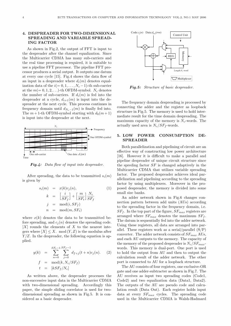
As shown in Fig.2, the output of FFT is input tothe despreader after the channel equalization. Sincethe Multicarrier CDMA has many sub-carriers andthe real time processing is required, it is suitable touse a pipeline FFT processor. The pipeline FFT pro-cessor produces a serial output. It outputs one datumat every one cycle [15]. Fig.4 shows the data flow ofan input in a despreader where di(m) denotes equal-ization data of the i(= 0, 1, . . . , Nc−1)-th sub-carrierat the m(= 0, 1, 2, . . .)-th OFDM-symbol. Nc denotesthe number of sub-carriers. If di(m) is fed into thedespreader at a cycle, di+1(m) is input into the de-spreader at the next cycle. This process continues infrequency domain until dNc−1(m) is finally fed into.The m+1-th OFDM-symbol starting with d0(m+1)is input into the despreader at the next.
Frequency
Time
Nc
One sub-carrier
One OFDM-symbol
One data: di(m )
Fig.4: Data flow of input into despreader.
After spreading, the data to be transmitted si(m)is given by
si(m) = x(k)cj(n), (1)
k =[ i
SFf
]+
[ m
SFt
] Nc
SFf
j = mod(i, SFf )n = mod(m,SFt)
where x(k) denotes the data to be transmitted be-fore spreading, and cj(n) denotes the spreading code.[X] rounds the elements of X to the nearest inte-gers where [X] ≤ X. mod (Y, Z) is the modulus afterY/Z. In the despreader, the following equation is ap-plied.
y(k) =SFt−1∑n=0
SFf−1∑j=0
df+j(t + n)cj(n). (2)
f = mod(k,Nc/SFf )t = [kSFf/Nc]
As written above, the despreader processes thenon-successive input data in the Multicarrier CDMAwith two-dimensional spreading. Accordingly thispaper, the simple sliding correlator is used for two-dimensional spreading as shown in Fig.5. It is con-sidered as a basic despreader.
Code:cj(n) Data:df+j(t+n)
REG
Mem
ory
Multiplexer
Length:Nc-word
Control Unit
Fig.5: Structure of basic despreader.
The frequency domain despreading is processed byconnecting the adder and the register as loopbackstructure in Fig.5. The memory is used to hold inter-mediate result for the time domain despreading. Themaximum capacity of the memory is Nc-words. Theactually used area is Nc/SFf -words.
5. LOW POWER CONSUMPTION DE-SPREADER
Both parallelization and pipelining of circuit are aneffective way of constructing low power architecture[16]. However it is difficult to make a parallel andpipeline despreader of unique circuit structure sincethe spreding factor SF is changed adaptively in theMulticarrier CDMA that utilizes variable spreadingfactor. The proposed despreader achieves ideal par-allelization and pipelining according to the spreadingfactor by using multiplexers. Moreover in the pro-posed despreader, the memory is divided into somesmall size banks.
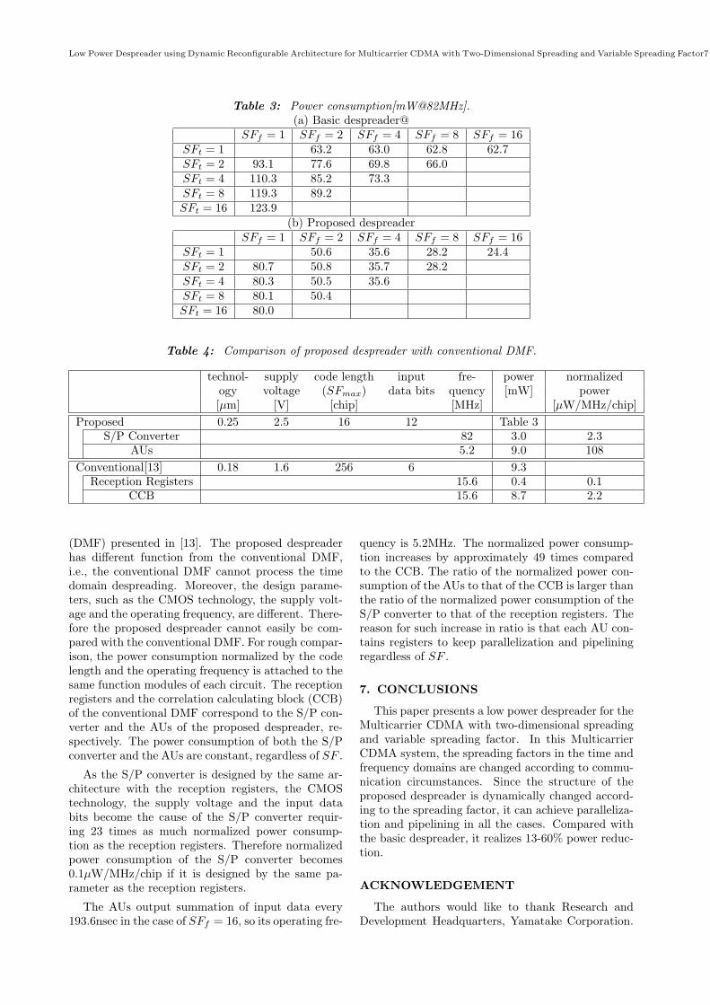
An adder network shown in Fig.6 changes con-nection pattern between add units (AUs) accordingto the spreading factor in the frequency domain, i.e.SFf . In the top part of the figure, SFmax registers arearranged where SFmax denotes the maximum SFf .The datum is sequentially fed into the adder network.Using these registers, all data are arranged into par-allel. These registers work as a serial/parallel (S/P)converter. The adder network consists of SFmax AUs,and each AU outputs to the memory. The capacity ofthe memory of the proposed despreader is Nc/SFmax-words. This memory is dual-port. One port is usedto hold the output from AU and then to output thecalculation result of the adder network. The otherport is connected to AU for a loopback structure.
The AU consists of four registers, one exclusive-ORgate and one adder-subtracter as shown in Fig.7. TheAU receives as input two spreading codes (Code1,Code2) and two equalization data (Data1, Data2).The outputs of the AU are pseudo code and calcu-lation result (Data Out). Each register holds inputdata at every SFmax cycles. The spreading codeused in the Multicarrier CDMA is Walsh-Hadmard
Low Power Despreader using Dynamic Reconfigurable Architecture for Multicarrier CDMA with Two-Dimensional Spreading and Variable Spreading Factor5
code whose value is ’+1’ or ’-1’. Therefore, multipli-cation between spreading code and equalization da-tum mentioned in Eq.(2) can be realized to changesign of equalization datum if spreading code is ’-1’.The adder-subtracter calculates Data2±Data1. Ad-dition or subtraction is selected according to the out-put of the exclusive-OR gate. If both Code1 andCode2 are ’+1’, then addition is selected. The pseudocode thus becomes ’+1’. If Code1 and Code2 are’-1’ and ’+1’, respectively, then subtraction is se-lected. The pseudo code thus becomes ’+1’. IfCode1 and Code2 are ’+1’ and ’-1’, respectively, thensubtraction is selected. The pseudo code thus be-comes ’-1’. The AU accordingly calculates -(Data2-Data1)=Data1-Data2. If both Code1 and Code2 are’-1’, then addition is selected. The pseudo code thusbecomes ’-1’.
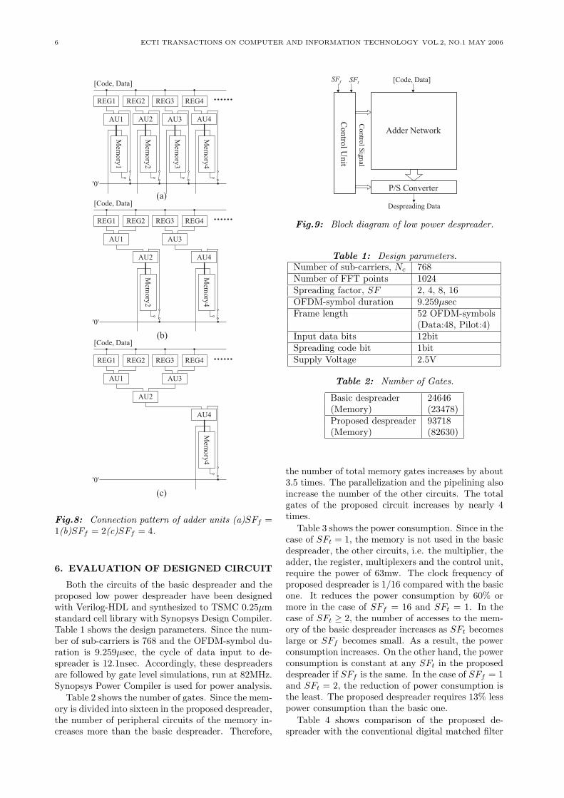
Input data of AU are controlled by multiplexer ac-cording to several SFf . In the case of SFf = 1,each AU is composed in parallel (Fig.8(a)). cj(n) anddf+j(t+n) are input into Code1 and Data1 shown inFig.7, respectively. In the case of SFf = 2, each AUis composed in two pipeline stages and SFmax/2 par-allel lines (Fig.8(b)). AU of the first pipeline stageprocesses the despreading in the frequency domain.AU of the second pipeline stage processes the timedomain despreading. In the case of SFf = 4, eachAU is composed in three pipeline stages and SFmax/4parallel lines (Fig.8(c)).
To summarize, the adder network is designed to
REG REG
/
REG REG
Data1 Data2 Code2Code1
Data Out Pseudo Code
[Code1, Data1] [Code2, Data2]
[Pseudo Code, Data Out]
Fig.7: Structure of add unit.
form the alignment of SFf AUs in log2 SFf + 1pipeline stages in SFmax/SFf parallel lines. AUswhich are arranged from the first to log2 SFf -thpipeline stages process the despreading in the fre-quency domain. The time domain despreading is pro-cessed by AU of the last pipeline stage and memory.
Fig.9 shows block diagram of the proposed lowpower despreader. The control unit generates signalscontrolling each module. Despreading data is selectedfrom outputs of all memories of the adder network bythe parallel/serial (P/S) converter according to thecontrol signal.
6 ECTI TRANSACTIONS ON COMPUTER AND INFORMATION TECHNOLOGY VOL.2, NO.1 MAY 2006
Mem
ory
1
AU1 AU2 AU3 AU4
Mem
ory
2
Mem
ory
3
Mem
ory
4
REG1 REG2 REG3 REG4
[Code, Data]
'0'
AU1
AU2
AU3
AU4
Mem
ory
2
Mem
ory
4
REG1 REG2 REG3 REG4
[Code, Data]
'0'
AU1
AU2
AU3
AU4
Mem
ory
4REG1 REG2 REG3 REG4
[Code, Data]
'0'
(a)
(b)
(c)
Fig.8: Connection pattern of adder units (a)SFf =1(b)SFf = 2(c)SFf = 4.
6. EVALUATION OF DESIGNED CIRCUIT
Both the circuits of the basic despreader and theproposed low power despreader have been designedwith Verilog-HDL and synthesized to TSMC 0.25µmstandard cell library with Synopsys Design Compiler.Table 1 shows the design parameters. Since the num-ber of sub-carriers is 768 and the OFDM-symbol du-ration is 9.259µsec, the cycle of data input to de-spreader is 12.1nsec. Accordingly, these despreadersare followed by gate level simulations, run at 82MHz.Synopsys Power Compiler is used for power analysis.
Table 2 shows the number of gates. Since the mem-ory is divided into sixteen in the proposed despreader,the number of peripheral circuits of the memory in-creases more than the basic despreader. Therefore,
Adder Network
Contro
l Unit
P/S Converter
Contro
l Sig
nal
SFf SFt [Code, Data]
Despreading Data
Fig.9: Block diagram of low power despreader.
Table 1: Design parameters.Number of sub-carriers, Nc 768Number of FFT points 1024Spreading factor, SF 2, 4, 8, 16OFDM-symbol duration 9.259µsecFrame length 52 OFDM-symbols
(Data:48, Pilot:4)Input data bits 12bitSpreading code bit 1bitSupply Voltage 2.5V
the number of total memory gates increases by about3.5 times. The parallelization and the pipelining alsoincrease the number of the other circuits. The totalgates of the proposed circuit increases by nearly 4times.
Table 3 shows the power consumption. Since in thecase of SFt = 1, the memory is not used in the basicdespreader, the other circuits, i.e. the multiplier, theadder, the register, multiplexers and the control unit,require the power of 63mw. The clock frequency ofproposed despreader is 1/16 compared with the basicone. It reduces the power consumption by 60% ormore in the case of SFf = 16 and SFt = 1. In thecase of SFt ≥ 2, the number of accesses to the mem-ory of the basic despreader increases as SFt becomeslarge or SFf becomes small. As a result, the powerconsumption increases. On the other hand, the powerconsumption is constant at any SFt in the proposeddespreader if SFf is the same. In the case of SFf = 1and SFt = 2, the reduction of power consumption isthe least. The proposed despreader requires 13% lesspower consumption than the basic one.
Table 4 shows comparison of the proposed de-spreader with the conventional digital matched filter
Low Power Despreader using Dynamic Reconfigurable Architecture for Multicarrier CDMA with Two-Dimensional Spreading and Variable Spreading Factor7
Table 3: Power consumption[mW@82MHz].(a) Basic despreader@
AUs 5.2 9.0 108Conventional[13] 0.18 1.6 256 6 9.3
Reception Registers 15.6 0.4 0.1CCB 15.6 8.7 2.2
(DMF) presented in [13]. The proposed despreaderhas different function from the conventional DMF,i.e., the conventional DMF cannot process the timedomain despreading. Moreover, the design parame-ters, such as the CMOS technology, the supply volt-age and the operating frequency, are different. There-fore the proposed despreader cannot easily be com-pared with the conventional DMF. For rough compar-ison, the power consumption normalized by the codelength and the operating frequency is attached to thesame function modules of each circuit. The receptionregisters and the correlation calculating block (CCB)of the conventional DMF correspond to the S/P con-verter and the AUs of the proposed despreader, re-spectively. The power consumption of both the S/Pconverter and the AUs are constant, regardless of SF .
As the S/P converter is designed by the same ar-chitecture with the reception registers, the CMOStechnology, the supply voltage and the input databits become the cause of the S/P converter requir-ing 23 times as much normalized power consump-tion as the reception registers. Therefore normalizedpower consumption of the S/P converter becomes0.1µW/MHz/chip if it is designed by the same pa-rameter as the reception registers.
The AUs output summation of input data every193.6nsec in the case of SFf = 16, so its operating fre-
quency is 5.2MHz. The normalized power consump-tion increases by approximately 49 times comparedto the CCB. The ratio of the normalized power con-sumption of the AUs to that of the CCB is larger thanthe ratio of the normalized power consumption of theS/P converter to that of the reception registers. Thereason for such increase in ratio is that each AU con-tains registers to keep parallelization and pipeliningregardless of SF .
7. CONCLUSIONS
This paper presents a low power despreader for theMulticarrier CDMA with two-dimensional spreadingand variable spreading factor. In this MulticarrierCDMA system, the spreading factors in the time andfrequency domains are changed according to commu-nication circumstances. Since the structure of theproposed despreader is dynamically changed accord-ing to the spreading factor, it can achieve paralleliza-tion and pipelining in all the cases. Compared withthe basic despreader, it realizes 13-60% power reduc-tion.
ACKNOWLEDGEMENT
The authors would like to thank Research andDevelopment Headquarters, Yamatake Corporation.
8 ECTI TRANSACTIONS ON COMPUTER AND INFORMATION TECHNOLOGY VOL.2, NO.1 MAY 2006
This work is supported by LSI Design and EducationCenter(VDEC), the University of Tokyo, and MO-SIS in collaboration with Synopsys, Inc. This workis supported in parts by Semiconductor TechnologyAcademic Research Center(STARC), Project J-17.
References
[1] F.Adachi, “Wireless Past and Future–EvolvingMobile Communications Systems–,” IEICETRANS, vol.E84-A, no.1, pp.55-60, Jan. 2001.
[2] Suk YH, Yeung KH, “Challenges in the migrationto 4G mobile systems,” IEEE Comm Magazine,vol.41, no.12, pp.54-59, Dec. 2003.
[3] Munoz M, Rubio CG, “A new model for ser-vice and application convergence in B3G/4G net-works,” IEEE Wireless Communications, vol.11,no.5, pp.6-12, Oct. 2004.
[4] K.Imai, W.Takita, S.Kano, A.Kodate , “An Ex-tension of 4G Mobile Networks towards the Ubiq-uitous Real Space,” IEICE TRANS, vol.E88-B,no.7, pp.2700-2708, Jul. 2005.
[5] K. Fazel, “Performance of CDMA/OFDM for mo-bile communication systems,” Proc. IEEE ICUPC’93, pp.975-979, Oct. 1993.
[6] A.Chouly, A.Brajel, S.Jourdan, “Orthogonal mul-ticarrier techniques applied to direct sequencespread spectrum CDMA systems,” Proc. IEEEGLOBECOM ’93, pp.1723-1728, Nov. 1993.
[7] V.M.DaSilva, E.S.Sousa, “Multicarrier orthogo-nal CDMA signals for quasi-synchronous commu-nication systems,” IEEE Journal on Selected Ar-eas in Comm, vol.12, no.5, pp.842-852, Jun. 1994.
[8] N.Maeda, H.Atarashi, S.Abeta, M.Sawahashi,“VSF-OFCDM Using Two-Dimensional Spread-ing and Its Performance,” IEICE Technical Re-port, RCS2002-61, pp.59-64, May. 2002 [InJapanese].
Takayuki Sugawara was born in Sap-poro, Japan on 1978. He received theB.S. and M.S. degrees from HokkaidoUniversity Sapporo, Japan, in 2000 and2002, respectively. He is currently adoctoral student in Hokkaido University.His research interests are in the fieldsof Mobile Communications and LSI Sys-tem Design. Mr. Sugawara is a memberof the Institute of Electrical and Elec-tronics Engineers (U.S.A.) and the Insti-
tute of Electronics, Information and Communication Engineers(Japan).
Yoshikazu Miyanaga was born inSapporo, Japan, on December 20, 1956.He received the B.S., M.S., and Dr. Eng.degrees from Hokkaido University, Sap-poro, Japan, in 1979, 1981, and 1986, re-spectively. He was a Research Associateat the Institute of Applied Electricity,Hokkaido University from 1983 to 1987,a lecturer of Electronic Engineering atFaculty of Engineering, Hokkaido Uni-versity from 1987 to 1988 and an Asso-
ciate Professor of Electronic Engineering at Faculty of Engi-neering, Hokkaido University from 1988 to 1997. He is cur-rently a Professor of Laboratory for Information Communi-cation Network, Division of Media and Network Technologiesat Graduate School of Information Science and Technology,Hokkaido University. His research interests are in the areasof digital signal processing, communication systems and par-allel/pipelined VLSI system. Dr. Miyanaga is a member ofthe Institute of Electrical and Electronics Engineers (U.S.A.),the Institute of Electronics, Information and CommunicationEngineers (Japan) and the Acoustical Society of Japan.