Low-Power High-Speed Current Mode Logic Using Tunnel-FETs Wei-Yu Tsai, Huichu Liu*, Xueqing Li, and Vijaykrishnan Narayanan Dept. of Computer Science and Engineering and *Dept. of Electrical Engineering, Pennsylvania State University, USA Email: [email protected], [email protected], [email protected], and [email protected]Abstract—Current mode logic (CML) circuits have been widely used in high-speed data transceivers. The lower-voltage-swing makes the switching speed of CML much higher than the static logic can achieve, so it is worthy to adopt the CML circuits at the cost of higher power consumption in the high- speed applications. In order to obtain a better power efficiency (F requency/power) in CML, it is critical to reduce the power consumption while maintaining the high operating frequency. This paper proposes an alternative approach by building the CML circuits with tunneling-field-effect-transistor (Tunnel FETs or TFETs) to achieve a high-throughput, low-voltage interface circuit design. By taking advantage of its steep subthreshold slope (less than 60 mV /dec), TFET exhibits the same on/off current ratio at the input voltage swing interval much lower than that of the MOSFETs, which enables the supply voltage scaling in CML circuits. For a design target data-rate (20 Gbps for multiplexer and 50 Gbps for buffer), our simulations show that the proposed TFET CML circuits are able to reduce the supply voltage from 0.6 V in conventional Si FinFET CML circuits to as low as 0.3 V while using the same constant tail current. As a result, a power consumption reduction of approximately 50% is achieved by the proposed TFET CML circuits, making the TFET CML approach a promising candidate for future low-power, high-performance applications. Index Terms—CML, high-frequency, low-power, low-voltage, TFET. I. I NTRODUCTION W ITH the development of the emerging mobile sys- tems, the communication speed, and correspondingly, the bandwidth of communication interface circuits between electronics devices, has been increasing rapidly. Meanwhile, lowing the power consumption for higher power efficiency has also become a key issue for those devices to extend the battery life and support the system operation with comparatively weaker power sources such as the RF power [1]–[4]. As a result, developing devices and circuits to design such low- power high-speed communication interfaces are intriguing for future applications. On the other hand, the low-power high-speed circuit inter- face design is a challenging task. Static logic has been consid- ered as a general approach for functional logic gates dealing with the bit-wise parallel data. However, the limited bandwidth of static logic circuits is not adequate for novel high-speed serial link interfaces. The high-speed transmitters with Current mode logic (CML) using BiCMOS and highelectron-mobility transistor (HEMT) technologies have been reported (SiGe [5], [6] and InP HEMT [7], [8] at speed of 50 Gbps and above). CML circuits with a smaller output swing have been adopted for a faster switching speed at the expense of relatively higher constant power consumption at low data rates. For those CML circuits, the power consumption is deter- mined by the constant-current and the supply voltage, which is independent of the operation frequency. Therefore, the CML is more competent in the high-speed applications than the static logic. As the power-reduction of the CML circuits cannot be achieved by decreasing the frequency, some works have focused on reducing the gate counts [9], [10] as an architecture-level low-power approach for CML. However, the single-gate power consumptions of these works are still high because those CML gates have to operate with a high supply voltage. The challenge of the supply voltage reduction in CML logic comes from reduced voltage difference between logic- 1 and logic-0, given the fact that the voltage level switch in CML logic is not full-swing (from VDD to GND). Hence, an aggressive scaling of the supply voltage will cause an increasing failure rate in the circuit operation, which becomes the main obstacle for power reduction of the CML logic. In this work, we propose a low-voltage approach to reduce the power consumption of CML by using the steep slope tunneling field effect transistors (Tunnel FETs or TFETs). Benefited from its sub - 60 mV /dec subthreshold swing, TFET has shown its prominent energy efficiency advantages for ultra-low power applications, especially at reduced supply voltage of 0.3 V and below. Many works have explored TFET-based applications, such as static logic [11], D-FF [12], and SRAM [13]. TFET based analog/RF applications have recently been explored by taking advantage of its unique device characteristics such as the high transconductance to current ratio (g m /I DS ), uni-directional operation, low voltage operation, etc. [14]–[16], where the TFET-based CML hasn’t been explored so far. By taking the advantages of its desired low voltage operation characteristics, we highlight the perfor- mance benefits of the TFET CML circuits under extremely low biasing voltages to extend the application spaces of the CML logic. The design aspects and operation analysis of TFET CML circuits are presented compared with the baseline Si FinFET CML circuits. The low-voltage CML design is beneficial to explore the high-speed communication functions of some advanced low-power technologies, such as low supply voltage bio-electronic devices [17], or environmental power harvesting devices [2]–[4]. In the rest of this paper, Section II introduces the charac- 978-1-4799-6016-3/14/$31.00 2014 IEEE
Transcript
Low-Power High-Speed Current Mode Logic UsingTunnel-FETs
Wei-Yu Tsai, Huichu Liu*, Xueqing Li, and Vijaykrishnan NarayananDept. of Computer Science and Engineering and *Dept. of Electrical Engineering, Pennsylvania State University, USA
Abstract—Current mode logic (CML) circuits have been widelyused in high-speed data transceivers. The lower-voltage-swingmakes the switching speed of CML much higher than thestatic logic can achieve, so it is worthy to adopt the CMLcircuits at the cost of higher power consumption in the high-speed applications. In order to obtain a better power efficiency(Frequency/power) in CML, it is critical to reduce the powerconsumption while maintaining the high operating frequency.This paper proposes an alternative approach by building theCML circuits with tunneling-field-effect-transistor (Tunnel FETsor TFETs) to achieve a high-throughput, low-voltage interfacecircuit design. By taking advantage of its steep subthreshold slope(less than 60 mV/dec), TFET exhibits the same on/off currentratio at the input voltage swing interval much lower than that ofthe MOSFETs, which enables the supply voltage scaling in CMLcircuits. For a design target data-rate (20 Gbps for multiplexerand 50 Gbps for buffer), our simulations show that the proposedTFET CML circuits are able to reduce the supply voltage from0.6 V in conventional Si FinFET CML circuits to as low as 0.3 Vwhile using the same constant tail current. As a result, a powerconsumption reduction of approximately 50% is achieved by theproposed TFET CML circuits, making the TFET CML approacha promising candidate for future low-power, high-performanceapplications.
Index Terms—CML, high-frequency, low-power, low-voltage,TFET.
I. INTRODUCTION
W ITH the development of the emerging mobile sys-tems, the communication speed, and correspondingly,
the bandwidth of communication interface circuits betweenelectronics devices, has been increasing rapidly. Meanwhile,lowing the power consumption for higher power efficiency hasalso become a key issue for those devices to extend the batterylife and support the system operation with comparativelyweaker power sources such as the RF power [1]–[4]. As aresult, developing devices and circuits to design such low-power high-speed communication interfaces are intriguing forfuture applications.
On the other hand, the low-power high-speed circuit inter-face design is a challenging task. Static logic has been consid-ered as a general approach for functional logic gates dealingwith the bit-wise parallel data. However, the limited bandwidthof static logic circuits is not adequate for novel high-speedserial link interfaces. The high-speed transmitters with Currentmode logic (CML) using BiCMOS and highelectron-mobilitytransistor (HEMT) technologies have been reported (SiGe [5],[6] and InP HEMT [7], [8] at speed of 50 Gbps and above).
CML circuits with a smaller output swing have been adoptedfor a faster switching speed at the expense of relatively higherconstant power consumption at low data rates.
For those CML circuits, the power consumption is deter-mined by the constant-current and the supply voltage, whichis independent of the operation frequency. Therefore, the CMLis more competent in the high-speed applications than thestatic logic. As the power-reduction of the CML circuitscannot be achieved by decreasing the frequency, some workshave focused on reducing the gate counts [9], [10] as anarchitecture-level low-power approach for CML. However, thesingle-gate power consumptions of these works are still highbecause those CML gates have to operate with a high supplyvoltage. The challenge of the supply voltage reduction in CMLlogic comes from reduced voltage difference between logic-1 and logic-0, given the fact that the voltage level switch inCML logic is not full-swing (from VDD to GND). Hence,an aggressive scaling of the supply voltage will cause anincreasing failure rate in the circuit operation, which becomesthe main obstacle for power reduction of the CML logic.
In this work, we propose a low-voltage approach to reducethe power consumption of CML by using the steep slopetunneling field effect transistors (Tunnel FETs or TFETs).Benefited from its sub − 60 mV/dec subthreshold swing,TFET has shown its prominent energy efficiency advantagesfor ultra-low power applications, especially at reduced supplyvoltage of 0.3 V and below. Many works have exploredTFET-based applications, such as static logic [11], D-FF [12],and SRAM [13]. TFET based analog/RF applications haverecently been explored by taking advantage of its uniquedevice characteristics such as the high transconductance tocurrent ratio (gm / IDS), uni-directional operation, low voltageoperation, etc. [14]–[16], where the TFET-based CML hasn’tbeen explored so far. By taking the advantages of its desiredlow voltage operation characteristics, we highlight the perfor-mance benefits of the TFET CML circuits under extremelylow biasing voltages to extend the application spaces of theCML logic. The design aspects and operation analysis ofTFET CML circuits are presented compared with the baselineSi FinFET CML circuits. The low-voltage CML design isbeneficial to explore the high-speed communication functionsof some advanced low-power technologies, such as low supplyvoltage bio-electronic devices [17], or environmental powerharvesting devices [2]–[4].
In the rest of this paper, Section II introduces the charac-978-1-4799-6016-3/14/$31.00 2014 IEEE
teristics of CML and TFET, respectively. Section III describeshow the TFET characteristics benefit the CML operation as thesupply voltage is reduced. Section IV presents the simulationresults of the TFET CML compared with the baseline SiFinFET designs, followed by the conclusion in Section V.
II. CURRENT MODE LOGIC AND TUNNEL FETA. Current Mode Logic Characteristics
The major difference between the CML circuits and thestatic logic circuits is that the CML has a voltage swingsmaller than the static logic, and thereby it has a shorterswitching time. The schematics of CML buffer and multiplexer(MUX) are shown in Fig. 1, respectively. A CML logic circuitis constructed by a constant current tail, several pairs oftransistors, and a pair of resistors. In a CML buffer, thereis only one pair of transistors, controlled by the differentialinputs. The resistors and NMOS’s are used to charge anddischarge the output node pair, OUTPUT . The logic ofOUTPUT is the inverse of that of INPUT , which controlsthe on/off state of the transistor pair. The voltage level is equalto the supply voltage (VSUPPLY ) when OUTPUT is logic-1,but it’s not the ground-level when logic-0. The total constantcurrent (IC) passes through one of the resistors, making thevoltage on the output node on that resistor drops to voltage oflogic-0 (V0):
V1 − V0 = R× IC . (1)
It is noted that the CML circuits consume approximately con-stant amount of power (VSUPPLY ×IC), and the consumptionis almost independent to the switching frequency of inputlogic.VSUPPLY of a CML buffer is distributed onto the three
components the current pass through, which are one of theresistors, one of the transistor pair, and the current tail.Specifically, the current tail is usually implemented by a singletransistor operating in the saturation region, so the currentpath would be considered as one resistor and two transistors.Similarly, the current in a CML MUX is selected by the lowertransistor pair (Pair−3), and then be selected again by one ofthe upper pairs (Pair− 1 or Pair− 2). Hence the VSUPPLY
of a CML MUX is distributed onto four components, whichare one resistor and three transistors.
The bias conditions of the transistors’ drain-to-source (VDS)and gate-to-source (VGS) voltages are the key aspects in CMLcircuit design. The VGS and the VDS are strictly relatedto the VSUPPLY because of the voltage distribution as dis-cussed above. In low-power design domain, there are severallimitations for the operation of transistors while VSUPPLY
is reduced. First of all, the CMOS transistors can operateproperly when VGS , which is related to the output voltageswing of the previous stage, is above the threshold voltage(VTH ). If the VSUPPLY of a CML circuit becomes too lowfor the voltage difference (V1 − V0) to be distinguishable, thesucceeding stage circuits might have an indistinct input logic,resulting in a small on/off current ratio. Secondly, reducingthe VSUPPLY might also lower the VDS of the current tail.
INPUT
OUTPUT
IC
R
VSUPPLY
IC*R
VDS
VTail
OUTPUT(On)
VDS
VTail
INPUT(On)
IC*R
VDS
VTail
INPUT(Off)
VDS
VTail
OUTPUT(Off)
VGS
VGS
V0
V1
1
(a)
INPUT 0 INPUT 1
SELECT
OUTPUT
Pair-1 Pair-2
Pair-3
IC
R
VSUPPLY
IC*R
VDS
OUTPUT
(OnOn)
VTail
VDS
VDS
VTail
VDS
OUTPUT
(OffOn)
VDS
VTail
VDS
OUTPUT
(On/OffOff)
V0
V1
2
(b)
Fig. 1. Schematics and voltage distributions of current mode logic (CML)(a) buffer and (b) multiplexer (MUX) circuits.
Because the current tail should be operated in the saturationregion in order to maintain a constant current insensitive tothe glitch of VDS , the aggressive reduction of VSUPPLY isdetrimental to the CML operation. Moreover, the lower theVSUPPLY is, the lower VGS and VDS the CMOS transistorsare operating with, and the more possibly the logic would failor slow down. Given this reason, the subthreshold or near-threshold CMOS designs are not suitable in low-power CMLcircuits.
Therefore, it is challenging to reduce the power consump-tion in CMOS CML circuits using the VSUPPLY scalingtechnique.
B. Tunnel FET Modeling and Device Characteristics
TFET has emerged as a promising alternative device tech-nology for various low power applications, benefiting forits sub-60 mV/decade subthreshold slope (SS) [18]. III-V material-based heterojunction TFET (HTFET) has furtherimproved tunneling current with the hetero-band alignment,exhibiting a comparable on-state current with the subthresholdMOSFET [19] with significant energy efficiency advantage.
As discussed in the Section II-A, to overcome the limitationof decreasing VSUPPLY of the CML circuits, a transistoroperates at a low supply voltage with high performance iscritical. Hence, we employ the GaSb-InAs HTFET in CML
1(State) is the state of the transistor, which might be turned on or off.2(Upper
Lower) are the states of the upper and lower transistors.
0.0 0.1 0.2 0.3 0.4 0.5 0.610
-3
10-2
10-1
100
101
102
103
60 mV/dec
VDS
=0.2, 0.4 V
HTFET
Si FinFET
I DS [A
/m
]
VGS
[V]
VDS
=0.1, 0.2 V30 mV/dec
(a)
GS
GS
(b)
Fig. 2. The current characteristics of different operating region for Si FinFETand HTFET: IDS vs. (a) VGS and (b) VDS .
0.0 0.2 0.4 0.6 0.80.0
0.1
0.2
0.3
0.4
0.5 HTFET V
DS=0.1V
HTFET VDS
=0.2V
Si FinFET VDS
=0.2V
Si FinFET VDS
=0.4V
CG
D [
fC/
m]
VGS
[V]
(a)
0.0 0.2 0.4 0.6 0.80.0
0.2
0.4
0.6
0.8
1.0 HTFET V
DS=0.1V
HTFET VDS
=0.2V
Si FinFET VDS
=0.2V
Si FinFET VDS
=0.4V
CG [
fC/
m]
VGS
[V]
(b)
Fig. 3. The capacitance characteristics of different operating regions forSi FinFET and HTFET: (a) CGD and (b) CG.
circuits, which is known as one of the most promising devicearchitectures to realize TFETs, to enable the further scaling theVSUPPLY . In this paper, we employ the 20 nm III-V HTFETVerilog-A model [20] developed from the TCAD Sentaurusdevice simulation [21] and calibrated by full-band accurateatomistic simulations [22], which has already been applied inprevious works [15], [23], [24]
A 20 nm Si FinFET Verilog-A model [20] is used as ourbaseline design for performance comparison.
Fig. 2(a) shows the IDS vs. VGS and IDS vs. VDS
characteristics of the modeled HTFET compared to 20 nmSi FinFET. The interband tunneling induced carrier injectionmechanism leads to a sub-60 mV/decade SS in TFET. Anaverage sub-threshold slope of 30 mV/decade can be achievedin HTFET at supply voltage VDS = 0.1 V and 0.2 V , whereits IDS outperforms that of the Si FinFET at VDS = 0.2 Vand 0.4 V below 0.5 V VGS . Besides the low voltageoperation, one of the most beneficial characteristic of HTFETfor CML circuits is the improved saturation characteristicscompared to Si FinFET, as shown in Fig. 2(b). Such charac-teristic has been recently observed in measured TFET outputcharacteristics in reported literature [25]. In circuit simulation,we carefully design the VDS bias of the current tail transistorto ensure the operation of TFET in saturation region to avoidthe variation of VDS during switching.
III. PROPOSED CML CIRCUITS IN HTFET
Given the fact that HTFET can operate with lower VGS
and VDS , in this section, we focus on the CML circuit design
using HTFETs to achieve low-power, high-speed operation.To analyze the performances of CML circuits in CMOS(Si FinFET is chosen as a comparable technology) and inHTFET, the buffer and the MUX circuits in this section areconstructed with the same structures as shown in Fig. 1.
A. Voltage Analysis for CML Buffer
When the VSUPPLY is lowered, the logic voltage swing(V1−V0) would also be reduced because of the lowered voltagedistributions on each component of CML circuits. Fig. 1(a)shows the ideal cases of voltage distributions of CML buffer instable status. The difference of input VGS , i.e. V1−V0, must belarge enough so that the on- and off-current are distinguishableto each other. In Fig. 2(a), the slope and corresponding currentof TFET at VGS = 0.15 V are similar to those of Si FinFETat VGS = 0.3 V , so 0.15 V is considered as the VTH of TFETand is a proper bias voltage as the cross point (midpoint oflogic-1 and logic-0). In other words, the current sensitivityto VGS is preserved when the HTFET is adopted in a biasVGS interval with an input swing 0.1 ∼ 0.2 V , comparedto the Si FinFET with 0.2 ∼ 0.4 V . Therefore, the VGS inon-state can be lowered to a half and the on-current is keptthe same. As a result, the proposed HTFET CML buffer canoperate correctly even when the VSUPPLY and voltage swingare reduced to one half of those in FinFET.
Another design constraint of CML circuits is that the bottomtransistor, which is used as the constant current tail, shouldprovide a stable current that is insensitive to the variation ofVDS . In the conventional CML circuit design, the current tailFinFET transistor is biased at the saturation region so that thecurrent is less sensitive to VDS . As shown in Fig. 2(b), theSi FinFET shows a higher gDS = ∆ IDS / ∆ VDS in thesaturation region due to the short channel effect. HTFETs, onthe other hand, exhibits a much lower gDS when the VDS
increases to the saturation region compared to Si FinFETs asdiscussed in Section II-B. Accordingly, the current tail in theproposed HTFET model can provide a more stable current thatis insensitive to the variation of VDS . In addition, the stabletail current and the differential signalling make the output ofthe CML circuits insensitive to peripheral noise.
B. Speed Analysis for CML Buffer
In CML circuits, the maximum operation frequency isdetermined by the charging and discharging time of the loadcapacitance. Figure 3 shows the capacitance characteristicsof Si FinFETs and HTFETs. The total parasitic capacitanceon the output node (CLOAD) is the sum of gate-to-draincapacitance (CGD) and gate capacitance (CG) times the fanoutnumber N. The HTFET has a smaller or equivalent CGD
and CG in the bias region (0.1V ∼ 0.2V ) compared tothe Si FinFETs in the respective region (0.2V ∼ 0.4V ).Moreover, because we use the similar IC for both Si FinFETand proposed HTFET based designs, the proposed HTFETCML circuit has a smaller charging time constant which is
proportional to the voltage swing,
Tcharge = R× CLOAD
= R× (CGD +N × CG). (2)
The discharging operation is through a different path, hencethe resistance of the transistors should be considered. Since thebias condition VDS varies with time, we use the equivalent RT
for the transistor resistance in the discharging time estimation,
Tdischarge = RT //R× CLOAD
= (VDS/IDS)//R× (CGD +N × CG). (3)
Ideally, the source voltage (VS) of the switching transistor pairis assumed to be steady because only one of them is turnedon due to the differential input. The drain-to-source currentIDS of the switching transistor pair varies with time. Forsimplicity, the current is assumed as the average IDS , which iscomparable for both Si FinFET and HTFET based designs. Asmentioned in Section III-A, the TFET in the proposed CMLconducts the similar current at a much lower biasing voltagethan the FinFET in the conventional CML. Accordingly, theproposed HTFET CML buffer can save power by reducingVSUPPLY , and it does not slow down the switching speedcompared to the Si FinFET CML buffer.
C. The CML Multiplexer
Compared to the CML buffer, the voltage distributions inthe CML MUX on every element are smaller, which imposesfurther challenges at reduced VSUPPLY . Figure 1(b) showsthat the additional voltage distribution on transistor Pair − 3in the CML MUX. Compared to the CML buffer, at the samevoltage swing, the VGS of Pair−1 or Pair−2 transistors inFig. 1(b) would be smaller due to the increased voltage levelof source-nodes of these transistors. Therefore, at the sameVSUPPLY , the voltage bias constraint of the CML MUX ismore restrictive than that of the CML buffer, especially whenVSUPPLY is reduced.
As shown in Fig. 2(a), the subthreshold slope of the HTFETis steeper than that of the Si FinFET when VGS < 0.1 V . If thebias VGS intervals are shifted left (because of the decreasedvoltage distributions in CML MUX) for both proposed HTFETand Si FinFET designs, the current IDS for discharging ofTFET might decrease slightly more than the current of FinFET.Consequently, the equivalent RT of a proposed HTFET CMLMUX might be increased more than that of a Si FinFETCML MUX. Fortunately, the ratio of VDS to IDS determinesthe time constant based on Eq. 3, where the proposed CMLMUX has the smaller VDS . If the voltage-current ratio for theproposed MUX is kept the same to that for the conventionalMUX, then the operation speed would be similar for bothdesigns.
For the Si FinFET CML MUX, the VGS must be largerthan VTH (about 0.3 V in this paper). According to Fig. 1(b),there are two more voltage distributions for the Pair − 3transistors and the current tail in addition to the VGS , so theCML circuits are hard to operate with VSUPLLY < 0.6 V . On
the contrary, the HTFET has an equivalent VTH (assuming theequivalent VTH of the HTFET is at IDS = 10 uA/um) about0.15 V , so the proposed CML circuits in HTFET is possibleto operate with a half VSUPPLY (0.3 V ). If the VSUPPLY
of the proposed HTFET CML MUX is further lowered, theIC would drop much faster than that of the conventional SiFinFET design, therefore the time constants (the charging anddischarging time) of proposed HTFET CML MUX would beincreased significantly. As a result, the lowest VSUPPLY forthe proposed HTFET CML circuits is 0.3 V .
In summary, the desired device operation of HTFET atlow bias voltages (VGS and VDS) is benificial to lower theVSUPPLY of high-speed CML circuits. The similar currentof HTFET at a much smaller VGS is important when theoutput swing is decreased. With a properly biased voltage, thetime constants of proposed HTFET CML circuits during thedischarging is less than or equal to those of the conventionalSi FinFET CML circuits, so the decreased VSUPPLY wouldnot slow down the operating speed. As a result, the proposedCML circuits in HTFET are capable to operate at the samespeed with a VSUPPLY about 0.3 V .
IV. SIMULATION RESULTS
In this section, we present the simulation results of theproposed HTFET CML buffer and CML MUX compared tothe Si FinFET designs, respectively. HTFET CML circuitscan operate with a much lower VSUPPLY at a similar highfrequency compared to the conventional CMOS-based (Si Fin-FET in this paper) CML circuits.
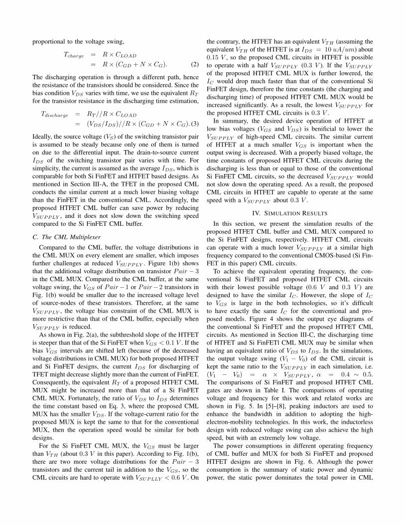
To achieve the equivalent operating frequency, the con-ventional Si FinFET and proposed HTFET CML circuitswith their lowest possible voltage (0.6 V and 0.3 V ) aredesigned to have the similar IC . However, the slope of ICto VGS is large in the both technologies, so it’s difficultto have exactly the same IC for the conventional and pro-posed models. Figure 4 shows the output eye diagrams ofthe conventional Si FinFET and the proposed HTFET CMLcircuits. As mentioned in Section III-C, the discharging timeof HTFET and Si FinFETl CML MUX may be similar whenhaving an equivalent ratio of VDS to IDS . In the simulations,the output voltage swing (V1 − V0) of the CML circuit iskept the same ratio to the VSUPPLY in each simulation, i.e.(V1 − V0) = α × VSUPPLY , α = 0.4 ∼ 0.5.The comparisons of Si FinFET and proposed HTFET CMLgates are shown in Table I. The comparisons of operatingvoltage and frequency for this work and related works areshown in Fig. 5. In [5]–[8], peaking inductors are used toenhance the bandwidth in addition to adopting the high-electron-mobility technologies. In this work, the inductorlessdesign with reduced voltage swing can also achieve the highspeed, but with an extremely low voltage.
The power consumptions in different operating frequencyof CML buffer and MUX for both Si FinFET and proposedHTFET designs are shown in Fig. 6. Although the powerconsumption is the summary of static power and dynamicpower, the static power dominates the total power in CML
V (mV)
600
550
500
450
400
350
3000 10 20 30 40
Time (ps)
(a) Conventional FinFET CML buffer @ 50 Gbps
0 10 20 30 40Time (ps)
V (mV)
250
225
200
175
150
125
100
275
(b) Proposed TFET CML buffer @ 50 Gbps
V (mV)
600
550
500
450
400
350
3000 25 50 75 100
Time (ps)
(c) Conventional FinFET CML MUX @ 20 Gbps
V (mV)
300
275
250
225
200
175
1500 25 50 75 100
Time (ps)
(d) Proposed TFET CML MUX @ 20 Gbps
Fig. 4. The output eye diagrams of buffer and MUX for conventional FinFETmodel vs. proposed TFET model.
circuits. The dynamic power for charging and dischargingtend to cancel the majority of each other and become smallbecause the CML circuit structure is symmetric and theINPUT and OUTPUT logic is differential. The proposedHTFET CML circuits operate under VSUPPLY = 0.3 V ,whereas the conventional Si FinFET CML circuits operate
TABLE ICOMPARISON OF CONVENTIONAL AND PROPOSED CML BUFFER AND
MUX GATES
Conventional CMLin FinFET
Proposed CMLin TFET
buffer MUX buffer MUXFrequency 50 Gbps 20 Gbps 50 Gbps 20 GbpsVSUPPLY 0.6 V 0.6 V 0.3 V 0.3 V
Power per gate 306 nW 213 nW 159 nW 103 nW
[1, 2] SiGe Multiplexer
[3, 4] InP Multiplexer
[5] RFID [10] Tree-Serializer
[9] MUX-FF Serializer
[11] TFET static logic [12]
TFET DFF
FinFET CML
TFET CML
0.1
1
10
0.5 5 50
Voltage (V)
Frequency (Gbps)
0.3
3
Fig. 5. The comparison of this work and related works in operating voltageand frequency.
under VSUPPLY = 0.6 V . Therefore, the power consumptionof proposed HTFET CML buffer is as low as about 1/2 tothat of the conventional Si FinFET design when they areworking at their highest frequency, which is 50 Gbps inthis simulation. Similarly, the power consumption ratio of theproposed HTFET to the conventional Si FinFET MUX is alsoabout 1/2 while working at 20 Gbps as shown in Fig. 6(b).In summary, the proposed HTFET CML buffer and MUXsave 48% and 52% power consumption in the simulations,respectively.
The experimental verification is currently not available dueto the infancy of the TFET process. Ongoing efforts arebeing carried out to improve the fabrication process for futureexperimental demonstrations of the TFET integrated chips.
V. CONCLUSION
In this paper, the high-speed CML circuits using heterojunc-tion TFET are proposed to reduce power consumption. Theproposed HTFET CML buffer and MUX circuits employ theconventional CMOS CML circuit designs with optimizationsof the bias conditions for performance improvement. Becausethe HTFET have a much lower effective threshold voltage(about 0.15 V ) and also a steep subthreshold slope, theproposed CML circuits are able to operate under a much lowersupply voltage compared to the baseline Si FinFET design(with threshold voltage about 0.3 V ). According to the voltageand speed analyses in Section III, the proposed HTFET CMLcircuits have a charging/discharging time constant less than orequal to that of the conventional Si FinFET designs with theproper design of the bias voltages, and therefore can operate
0
50
100
150
200
250
300
350
1.67 5.00 16.67 50.00
ProposedCML buffer(TFET)
ConventionalCML buffer(FinFET)
Power (nW)
Frequency (Gbps)
48% power saved@ 50 Gbps
(a)
0
50
100
150
200
250
0.67 2.00 6.67 20.00
ProposedCML MUX(TFET)
ConventionalCML MUX(FinFET)
Frequency (Gbps)
Power (nW) 52% power saved@ 20 Gbps
(b)
Fig. 6. The Power consumption under different frequency for conventionalFinFET and proposed TFET CML (a) buffer and (b) MUX circuits.
with much lower power consumption without degrading thespeed. The simulation results in Section IV have shown thatthe proposed HTFET CML circuits can operate with a supplyvoltage as low as 0.3 V at the same frequencies compared tothe conventional Si FinFET CML circuits (50 Gbps for thebuffer and 20 Gbps for the MUX). Meanwhile, the powerconsumption reduction is about 50% (because the supplyvoltage is reduced by half) when the HTFET is adopted inthe CML buffer and the MUX. The sequential CML circuits(latches or flip-flops), which have more design constraints inclock timing, are part of the prospective future works.
ACKNOWLEDGEMENTS
This work was supported in part by the LEAST, one ofthe six SRC STARnet Centers, sponsored by MARCO andDARPA. The NSF award 1317560 supported equipment isused in this effort.
REFERENCE
[1] D. De Donno, L. Catarinucci, and L. Tarricone, “A battery-assistedsensor-enhanced RFID tag enabling heterogeneous wireless sensor net-works,” Sensors Journal, IEEE, vol. 14, no. 4, pp. 1048–1055, April2014.
[2] S. Gollakota, M. Reynolds, J. Smith, and D. Wetherall, “The emergenceof RF-powered computing,” Computer, vol. 47, no. 1, pp. 32–39, Jan2014.
[3] H. Visser and R. Vullers, “RF energy harvesting and transport forwireless sensor network applications: Principles and requirements,”Proceedings of the IEEE, vol. 101, no. 6, pp. 1410–1423, June 2013.
[4] C. Alippi and C. Galperti, “An adaptive system for optimal solar energyharvesting in wireless sensor network nodes,” Circuits and Systems I:Regular Papers, IEEE Transactions on, vol. 55, no. 6, pp. 1742–1750,July 2008.
[5] M. Meghelli, A. Rylyakov, and L. Shan, “50-Gb/s SiGe BiCMOS 4:1multiplexer and 1:4 demultiplexer for serial communication systems,”Solid-State Circuits, IEEE Journal of, vol. 37, no. 12, pp. 1790–1794,Dec 2002.
[6] Y. Luo, G. Chen, and K. Zhou, “60Gb/s low jitter 4:1 mux and 1:4demux,” in Circuits and Systems, 2008. MWSCAS 2008. 51st MidwestSymposium on, Aug 2008, pp. 590–593.
[7] T. Suzuki, T. Takahashi, K. Makiyarna, K. Sawada, Y. Nakasha,T. Hirose, and M. Takikawa, “Under 0.5W 50Gb/s full-rate 4:1 MUXand 1:4 DEMUX in 0.13 µm InP HEMT technology,” in Solid-StateCircuits Conference, 2004. Digest of Technical Papers. ISSCC. 2004IEEE International, Feb 2004, pp. 234–525 Vol.1.
[8] T. Suzuki, Y. Kawano, Y. Nakasha, S. Yamaura, T. Takahashi,K. Makiyama, and T. Hirose, “A 50-Gbit/s 450-mW full-rate 4:1multiplexer with multiphase clock architecture in 0.13 µm InP HEMTtechnology,” Solid-State Circuits, IEEE Journal of, vol. 42, no. 3, pp.637–646, March 2007.
[9] H. Lu, C. Su, and C.-N. Liu, “A tree-topology multiplexer for mul-tiphase clock system,” Circuits and Systems I: Regular Papers, IEEETransactions on, vol. 56, no. 1, pp. 124–131, Jan 2009.
[10] W.-Y. Tsai, C.-T. Chiu, J.-M. Wu, S. Hsu, and Y.-S. Hsu, “A novel lowgate-count pipeline topology with multiplexer-flip-flops for serial link,”Circuits and Systems I: Regular Papers, IEEE Transactions on, vol. 59,no. 11, pp. 2600–2610, Nov 2012.
[11] U. Avci, R. Rios, K. Kuhn, and I. Young, “Comparison of performance,switching energy and process variations for the TFET and MOSFET inlogic,” in VLSI Technology (VLSIT), 2011 Symposium on, June 2011,pp. 124–125.
[12] M. Cotter, H. Liu, S. Datta, and V. Narayanan, “Evaluation of TunnelFET-based flip-flop designs for low power, high performance applica-tions,” in Quality Electronic Design (ISQED), 2013 14th InternationalSymposium on, March 2013, pp. 430–437.
[13] R. Pandey, V. Saripalli, J. Kulkarni, V. Narayanan, and S. Datta, “Impactof single trap random telegraph noise on Heterojunction TFET SRAMstability,” Electron Device Letters, IEEE, vol. 35, no. 3, pp. 393–395,March 2014.
[14] A. Trivedi, S. Carlo, and S. Mukhopadhyay, “Exploring tunnel-FETfor ultra low power analog applications: A case study on operationaltransconductance amplifier,” in Design Automation Conference (DAC),2013 50th ACM / EDAC / IEEE, 2013, pp. 1–6.
[15] H. Liu, R. Vaddi, S. Datta, and V. Narayanan, “Tunnel FET-basedultra-low power, high-sensitivity UHF RFID rectifier,” in Low PowerElectronics and Design (ISLPED), 2013 IEEE International Symposiumon, 2013, pp. 157–162.
[16] X. Li, H. Liu, K. Ma, U. Heo, S. Datta, and V. Narayanan, “RF-poweredsystems using steep-slope devices,” accepted by 12th IEEE InternationalNEW Circuits and Systems Conference (NEWCAS14), June 2014.
[17] Y. Sundarasaradula and A. Thanachayanont, “A 0.7-V, 2.86-µW low-noise logarithmic amplifier for neural recording system,” in TENCON2013 - 2013 IEEE Region 10 Conference (31194), Oct 2013, pp. 1–4.
[18] A. C. Seabaugh and Q. Zhang, “Low-voltage tunnel transistors forbeyond CMOS Logic,” Proceedings of the IEEE, vol. 98, no. 12, pp.2095–2110, 2010.
[19] D. Nikonov and I. Young, “Uniform methodology for benchmarkingbeyond-CMOS logic devices,” in Electron Devices Meeting (IEDM),2012 IEEE International, 2012, pp. 25.4.1–25.4.4.
[20] V. Saripalli, G. Sun, A. Mishra, Y. Xie, S. Datta, and V. Narayanan,“Exploiting heterogeneity for energy efficiency in chip multiprocessors,”Emerging and Selected Topics in Circuits and Systems, IEEE Journalon, vol. 1, no. 2, pp. 109–119, 2011.
[21] Synopsys, TCAD Sentaurus Device Manual, 2010.[22] U. Avci, S. Hasan, D. Nikonov, R. Rios, K. Kuhn, and I. Young,
“Understanding the feasibility of scaled III-V TFET for logic by bridgingatomistic simulations and experimental results,” in VLSI Technology(VLSIT), 2012 Symposium on, June 2012, pp. 183–184.
[23] H. Liu, M. Shoaran, X. Li, S. Datta, and V. Narayanan, “TunnelFET-based ultra-low power, low-noise amplifier design for bio-signalacquisition,” in Low Power Electronics and Design (ISLPED), 2014IEEE International Symposium on, 2014.
[24] X. Li, H. Liu, U. D. Heo, K. Ma, S. Datta, and V. Narayanan, “Rf-powered systems using steep-slope devices,” in IEEE International NewCircuits and Systems Conference (NEWCAS 2014), 2014.
[25] R. Rooyackers, A. Vandooren, A. Verhulst, A. Walke, K. Devriendt,S. Locorotondo, M. Demand, G. Bryce, R. Loo, A. Hikavyy, T. Van-deweyer, C. Huyghebaert, N. Collaert, and A. Thean, “A new com-plementary hetero-junction vertical Tunnel-FET integration scheme,” inElectron Devices Meeting (IEDM), 2013 IEEE International, Dec 2013,pp. 4.2.1–4.2.4.