83
Low Power Multistage Amplifiers For Large Capacitive Loads A M S C By Xiaohua Fan Chinmaya Mishra Edgar Sánchez-Sinencio See March 2005 issue in the IEEE JSSC

Low Power Multistage
Amplifiers
For Large Capacitive Loads
A M S C
By
Xiaohua Fan
Chinmaya Mishra
Edgar Sánchez-Sinencio
See March 2005 issue in the IEEE JSSC
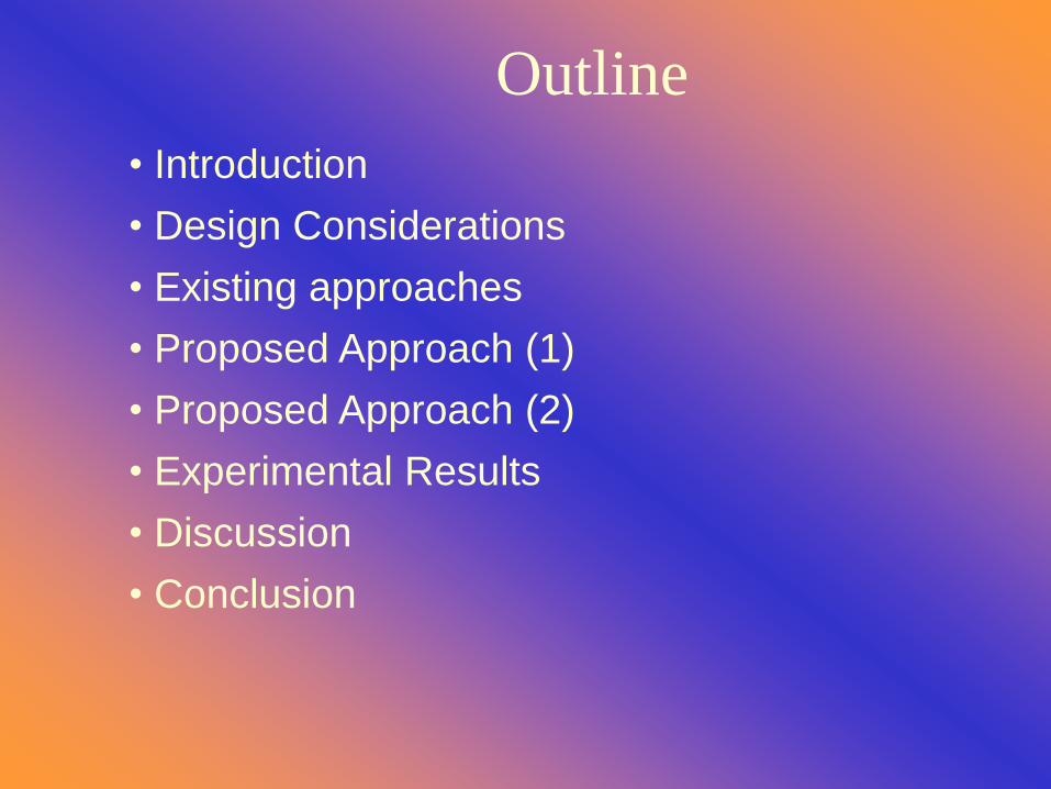
Outline
• Introduction
• Design Considerations
• Existing approaches
• Proposed Approach (1)
• Proposed Approach (2)
• Experimental Results
• Discussion
• Conclusion
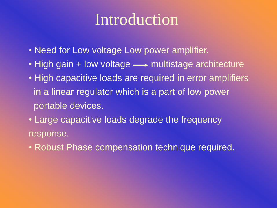
Introduction
• Need for Low voltage Low power amplifier.
• High gain + low voltage multistage architecture
• High capacitive loads are required in error amplifiers
in a linear regulator which is a part of low power
portable devices.
• Large capacitive loads degrade the frequency
response.
• Robust Phase compensation technique required.

Design Considerations• Large Capacitive Load
• Low Power
• Less Area
• High Gain
• Moderate GBW and PM
Existing solutions in the
literature?
+ -
gmL
-
Cm1
Cm2
gm1
gm2 C
L
Vin V
o
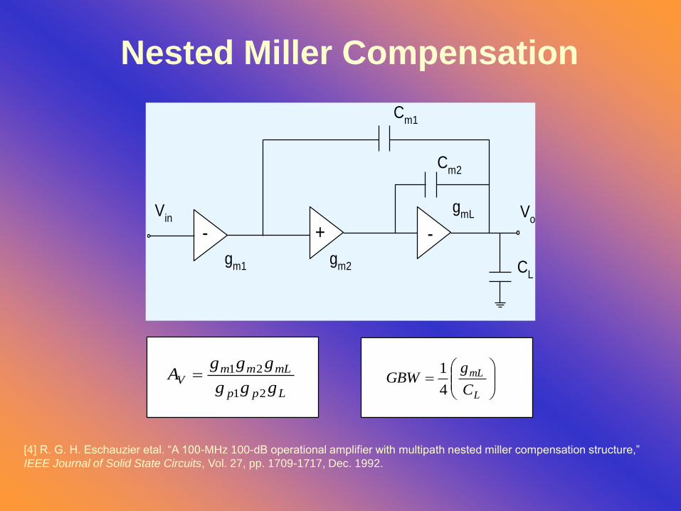
Nested Miller Compensation
Lpp
mLmmV
ggg
gggA
21
21
L
mL
C
gGBW
4
1
[4] R. G. H. Eschauzier etal. “A 100-MHz 100-dB operational amplifier with multipath nested miller compensation structure,”
IEEE Journal of Solid State Circuits, Vol. 27, pp. 1709-1717, Dec. 1992.

NMC (contd..)Stability analysis:
LmL
mm
LmL
mm
mmmL
Cg
gC
Cg
gC
ggg
22
11
21
2
4
,
324
1
2
1ppGBW
L
mL
m
m
m
m
C
g
C
g
C
g
4
1
2
1
2
2
1
1
Stability condition:
Cm1 and Cm2 very
large for large load!!
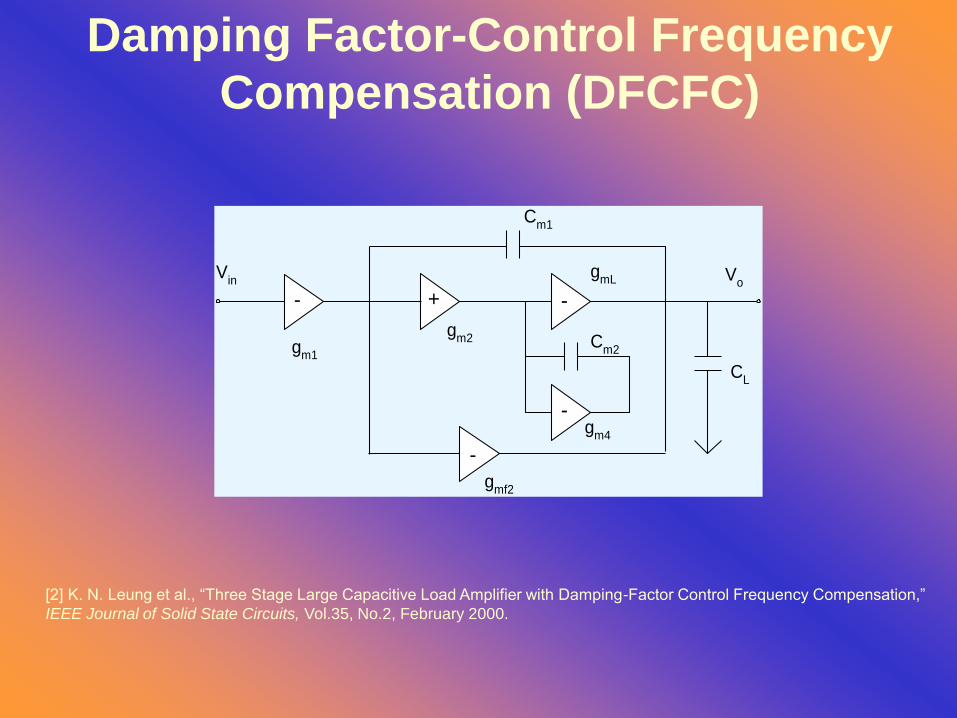
Damping Factor-Control Frequency
Compensation (DFCFC)
+ -
-
-
gm2
gmL
CL
gm4
gmf2
Vo
Vin
-
gm1
Cm1
Cm2
[2] K. N. Leung et al., “Three Stage Large Capacitive Load Amplifier with Damping-Factor Control Frequency Compensation,”
IEEE Journal of Solid State Circuits, Vol.35, No.2, February 2000.
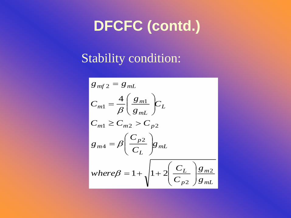
DFCFC (contd.)
mL
m
p
L
mLL
p
m
pmm
LmL
mm
mLmf
g
g
C
Cwhere
gC
Cg
CCC
Cg
gC
gg
2
2
2
4
221
11
2
211
4
Stability condition:
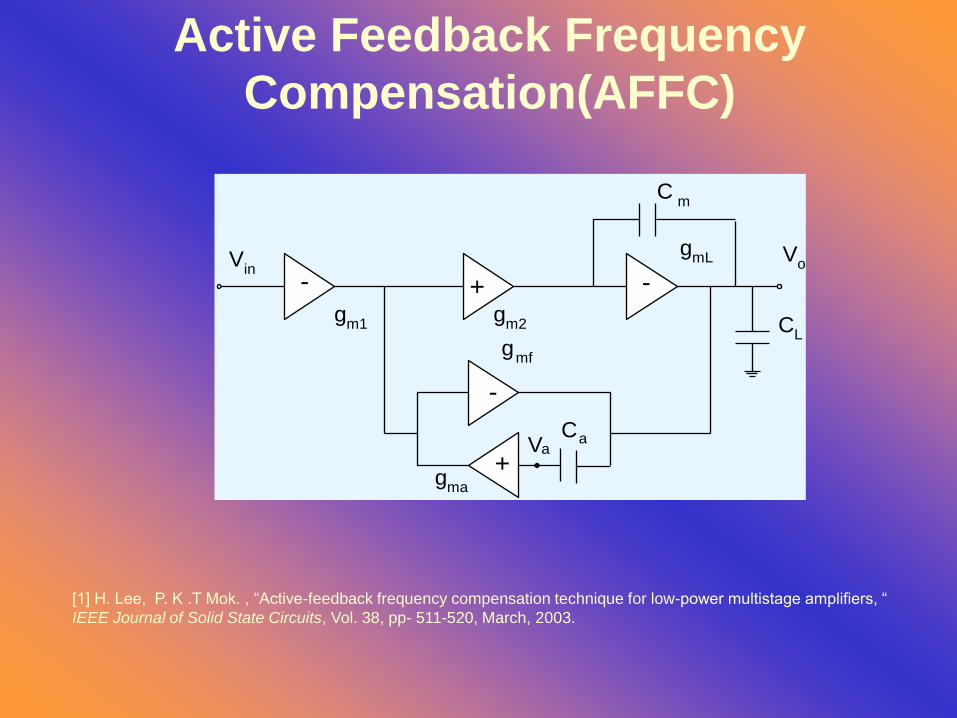
Active Feedback Frequency
Compensation(AFFC)
+ -
gmL
-
Cm
gm1
gm2 C
L
Vin
Vo
gmf
-
+Va
gma
Ca
[1] H. Lee, P. K .T Mok. , “Active-feedback frequency compensation technique for low-power multistage amplifiers, “
IEEE Journal of Solid State Circuits, Vol. 38, pp- 511-520, March, 2003.
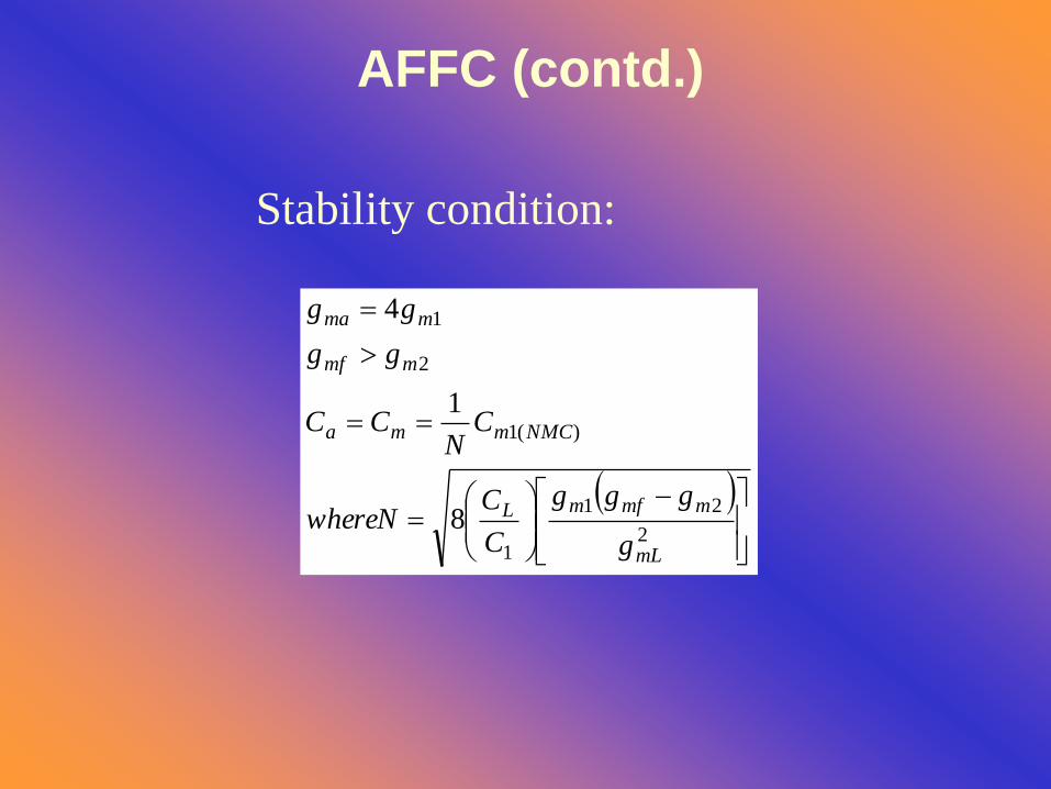
AFFC (contd.)
2
21
1
)(1
2
1
8
1
4
mL
mmfmL
NMCmma
mmf
mma
g
ggg
C
CwhereN
CN
CC
gg
gg
Stability condition:

Proposed Solution 1
Single Miller Capacitor (SMC)
CL
+ -
gm2
Vo
-
gm1
RL
Cp1
Cp2R
p1R
p2
Cm
Vin
-
gmL
gmf
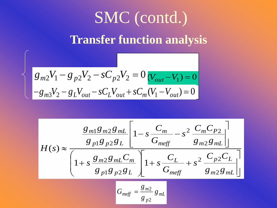
SMC (contd.)
Transfer function analysis
0)( 111111 VVsCVsCVgVg outmppinm0222212 VsCVgVg ppm
0)( 123 outmoutLoutLm VVsCVsCVgVg
mLm
Lp
meff
L
Lpp
mmLm
mLm
Pm
meff
m
Lpp
mLmm
gg
CCs
G
Cs
ggg
Cggs
gg
CCs
G
Cs
ggg
ggg
sH
2
22
21
2
2
22
21
21
11
1
)(
mLp
mmeff g
g
gG
2
2

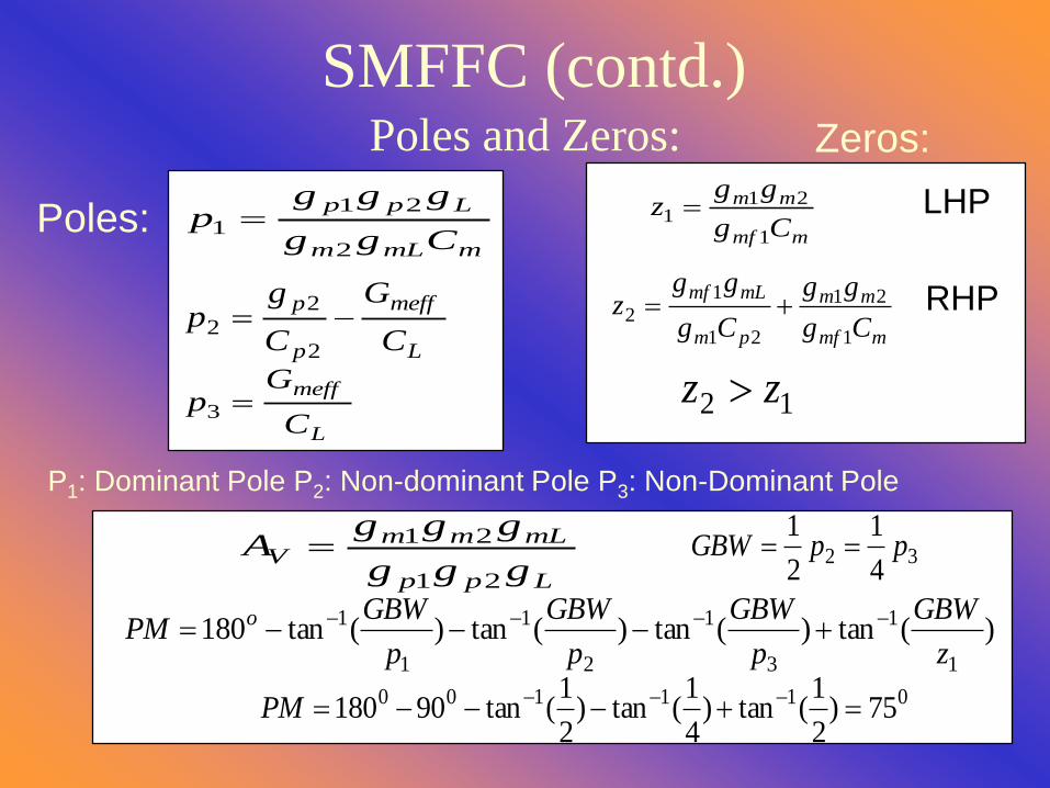
SMC (contd.)Poles and Zeros:
Poles:mmLm
Lpp
Cgg
gggp
2
21
1
L
meff
p
p
C
G
C
gp
2
2
2
L
meff
C
Gp 3
Zeros:m
meff
C
Gz 1
m
meff
p
p
C
G
C
gz
2
2
2
RHP
LHP
3,2,112 pzz
P1: Dominant Pole P2: Non-dominant Pole P3: Non-Dominant Pole
Lpp
mLmmV
ggg
gggA
21
21
)(tan)(tan)(tan1803
1
2
1
1
1
p
GBW
p
GBW
p
GBWPM o
324
1
2
1ppGBW 01100 4.49)
4
1(tan)
2
1(tan90180 PM
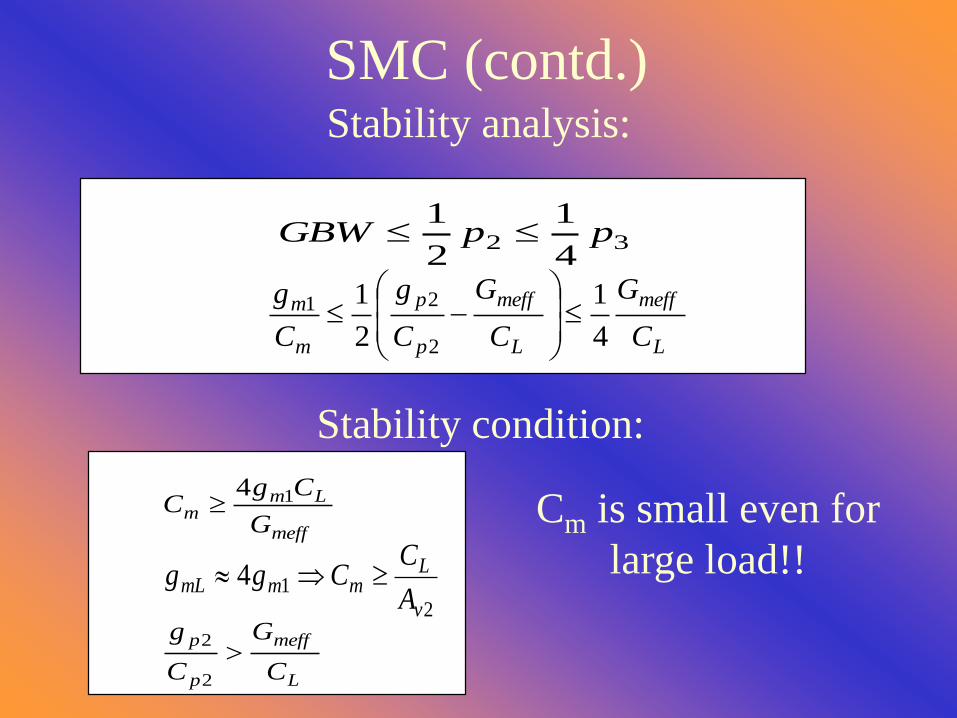
SMC (contd.)Stability analysis:
324
1
2
1ppGBW
L
meff
L
meff
p
p
m
m
C
G
C
G
C
g
C
g
4
1
2
1
2
21
Stability condition:
meff
Lmm
G
CgC 14
214
v
LmmmL
A
CCgg
L
meff
p
p
C
G
C
g
2
2
Cm is small even for
large load!!
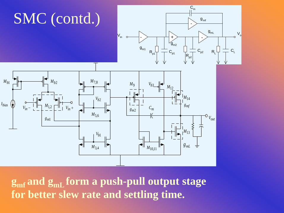
SMC (contd.)
inV inV2,1M
4,3M
6,5M
8,7M9M
11,10M
2bV
1bV
12M
13M
14M
3bV
outV
mC
1bM 2bM
biasI
1mg
2mg
mLg
mfg
gmf and gmL form a push-pull output stage
for better slew rate and settling time.
CL
+ -
gm2
Vo
-
gm1
RL
Cp1
Cp2R
p1R
p2
Cm
Vin
-
gmL
gmf

Proposed Solution 2
Single Miller Capacitor Feedforward
Compensation (SMFFC)
CL
+ -
gm2
gmL V
o-
gm1
RL
-
gmf2
Cp1
Cp2R
p1R
p2
Cm
-
gmf1
Vin
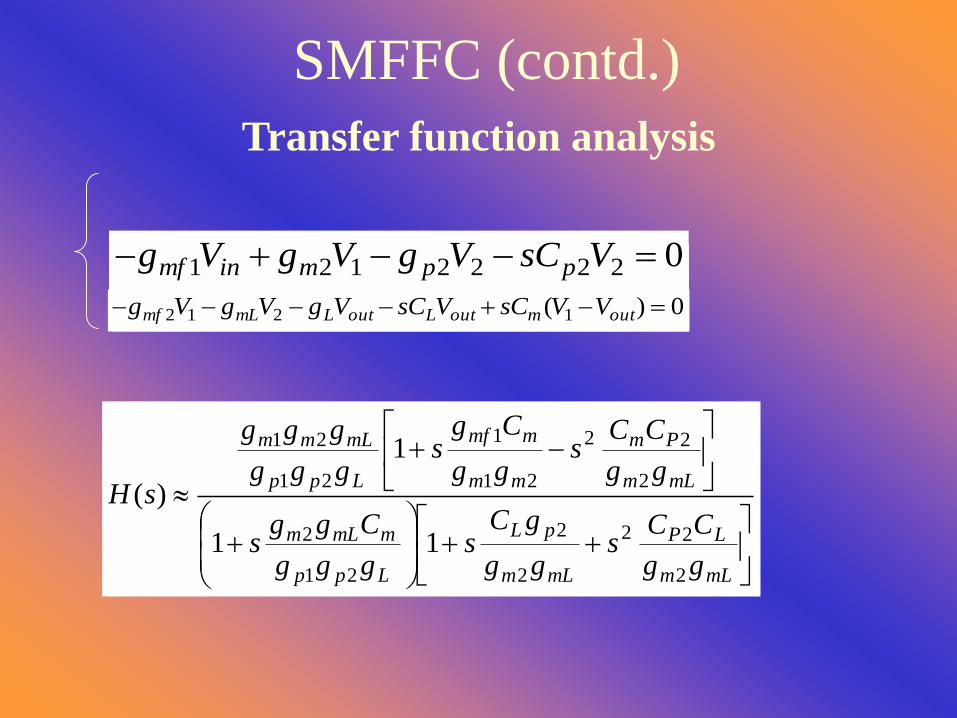
SMFFC (contd.)
Transfer function analysis
0)( 111111 VVsCVsCVgVg outmppinm02222121 VsCVgVgVg ppminmf
0)( 12312 outmoutLoutLmmf VVsCVsCVgVgVg
mLm
LP
mLm
pL
Lpp
mmLm
mLm
Pm
mm
mmf
Lpp
mLmm
gg
CCs
gg
gCs
ggg
Cggs
gg
CCs
gg
Cgs
ggg
ggg
sH
2
22
2
2
21
2
2
22
21
1
21
21
11
1
)(
0)( 1212 outmoutLoutLmLmf VVsCVsCVgVgVg
SMFFC (contd.)Poles and Zeros:
Poles:mmLm
Lpp
Cgg
gggp
2
21
1
L
meff
p
p
C
G
C
gp
2
2
2
L
meff
C
Gp 3
Zeros:
LHP
RHP
12 zz
P1: Dominant Pole P2: Non-dominant Pole P3: Non-Dominant Pole
Lpp
mLmmV
ggg
gggA
21
21
)(tan)(tan)(tan)(tan1801
1
3
1
2
1
1
1
z
GBW
p
GBW
p
GBW
p
GBWPM o
324
1
2
1ppGBW
011100 75)2
1(tan)
4
1(tan)
2
1(tan90180 PM
mmf
mm
Cg
ggz
1
211
mmf
mm
pm
mLmf
Cg
gg
Cg
ggz
1
21
21
1
2
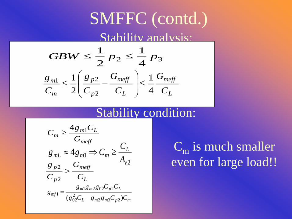
SMFFC (contd.)Stability analysis:
Stability condition:
Cm is much smaller
even for large load!!
meff
Lmm
G
CgC 14
214
v
LmmmL
A
CCgg
L
meff
p
p
C
G
C
g
2
2
mpmmL
Lpmm
mfCCggCg
CCgggg
)( 232202
20221
1
324
1
2
1ppGBW
L
meff
L
meff
p
p
m
m
C
G
C
G
C
g
C
g
4
1
2
1
2
21

SMFFC (contd.)
inV inV2,1M
4,3M
6,5M
8,7M9M
11,10M
2bV
1bV
12M
13M
14M
3bV
outV
mC
1bM 2bM
biasI
1mg
2mg
3mg
2mfg
inV inV2,1fM
1mfg
bV
bV 3bM
SchematicC
L
+ -
gm2
gmL V
o-
gm1
RL
-
gmf2
Cp1
Cp2R
p1R
p2
Cm
-
gmf1
Vin
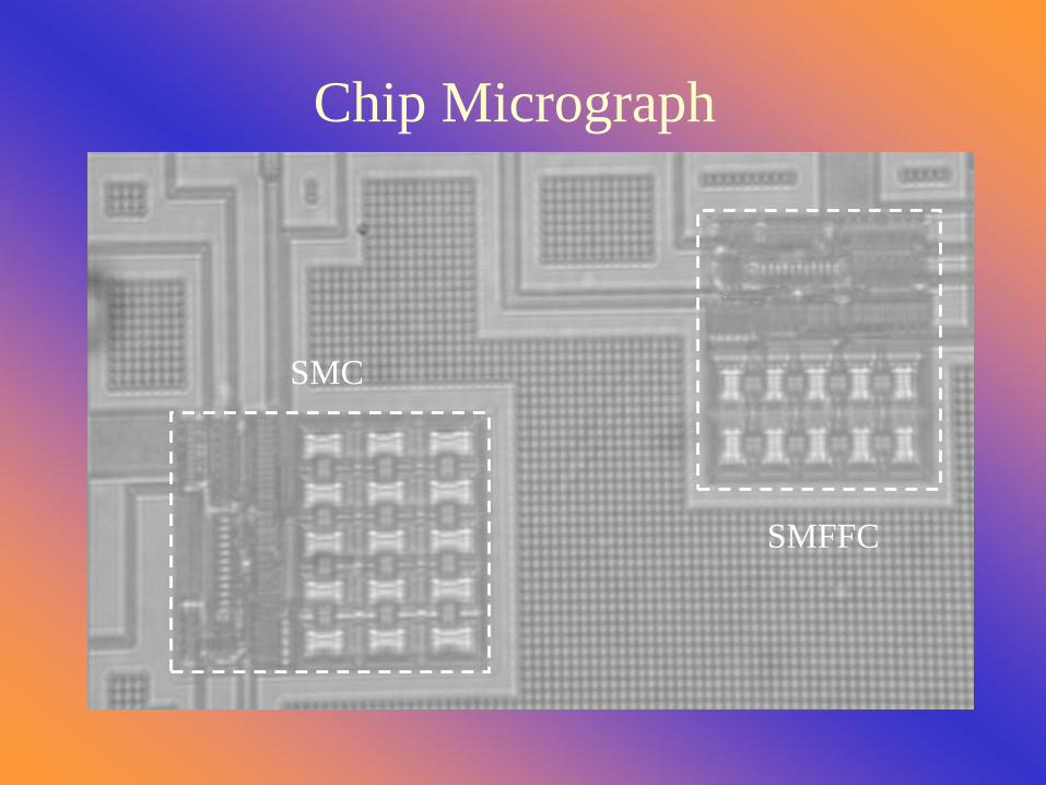
Chip Micrograph
SMC
SMFFC
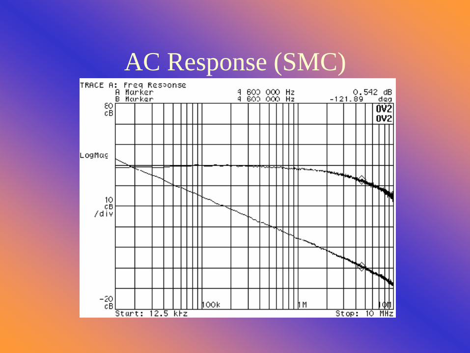
AC Response (SMC)
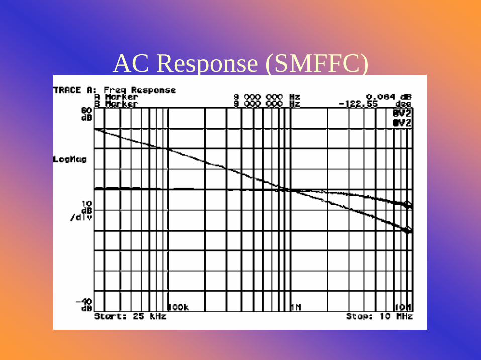
AC Response (SMFFC)
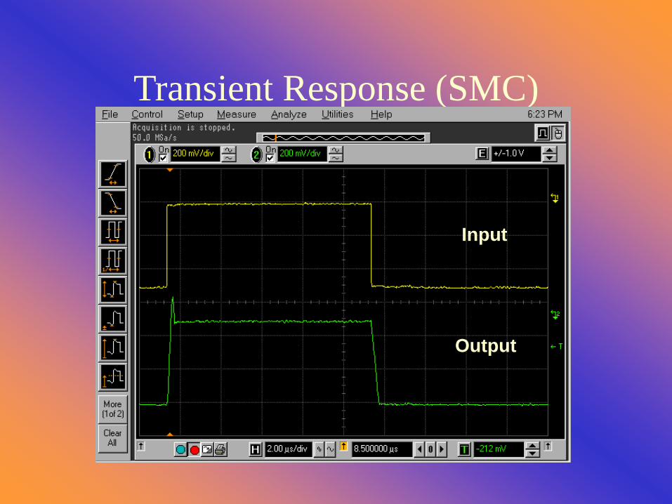
Transient Response (SMC)
Input
Output
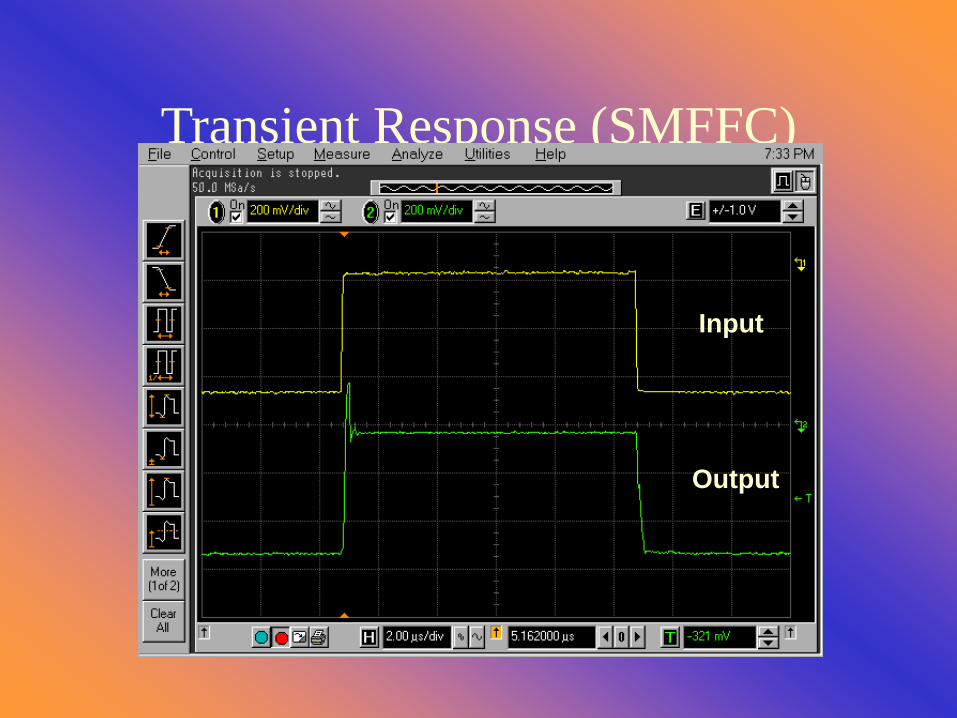
Transient Response (SMFFC)
Input
Output

Comparison Table NMC
DFCFC
AFFC
SMC
This Work
SMFFC
This Work
Load pF/KΩ 1 2 0 / 2 5 1 0 0 / 2 5 1 2 0 / 2 5 1 2 0 / 2 5 1 2 0 / 2 5
P o w e r S u p p l y 1V
DC gain (dB) >100 >100 >100 >100 >100
GBW (MHz) 0.4 2.6 4.5 4.6 9
Phase margin 61 o 43
o 65
o 57
o 57
o
Power (mW@Vdd) 0.38 @2 0.42 @2 0.4 @2 0.38@2 0.41@2
Capacitor Value
(pF)
Cm1=88
Cm2=11
Cm1=18
Cm2=3
Cm=3
Ca=7
Cm=7
Cm=4
Slew Rate
SR+/ SR- (V/S)
0.15/0.13 1.36/1.27 2.20/0.78 3.28/1.31 4.8/2
Settling Time
TS+/TS
- (s) (to 1%)
4.9/4.7 0.96/1.37 0.42/0.85 0.53/0.4 0.58/0.43
FOMS(MHz.pF/mW) 127 619 1350 1453 2634
FOML(V/s.pF/mW) 45 314 447 726 996
Area (mm2) 0.14 0.11 0.06 0.02 0.015
Normalized Area 9.33 7.33 4 1.33 1
Technology 0.8m
CMOS
0.5m
CMOS
Note: Average value of the slew rate is used in the calculation of FOML parameter
Power
CGBWFOM L
S
* and
Power
CSRFOM L
L
* , where CTotal = Total value of compensation
capacitors
Conclusions
Two low power multistage amplifier topologies are
introduced for large capacitive loads.
Performance parameters such as GBW and Area
are improved without sacrificing same power
consumption.
Pole splitting and feedforward approaches are
combined for better performance.
The proposed approaches have better small-
signal and large-signal performances than other
reported compensation topologies .

A Robust Feedforward
Compensation Scheme for Multi-
Stage OTA’s with no Miller
capacitors
Thanks to Bharath Kumar Thandri and
Dr José-Silva Martínez for the material provided
ELEN 607 (ESS)
Outline
• Need for high performance amplifiers
• Conventional approaches and problems
• Proposed NCFF compensation scheme
• Pole-zero mismatch effects
• OTA design
• Simulation and Experimental results
• Conclusion
11
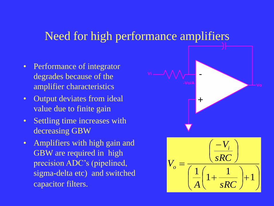
11
sRCA
sRC
V
V
i
o
Need for high performance amplifiers
• Performance of integrator
degrades because of the
amplifier characteristics
• Output deviates from ideal
value due to finite gain
• Settling time increases with
decreasing GBW
• Amplifiers with high gain and
GBW are required in high
precision ADC’s (pipelined,
sigma-delta etc) and switched
capacitor filters.
-
+
Vi
Vo-Vo/A
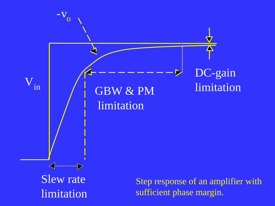
Slew rate
limitation
GBW & PM
limitation
DC-gain
limitationV
in
-vo
Step response of an amplifier with
sufficient phase margin.
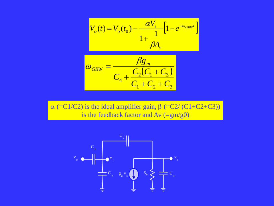
(=C1/C2) is the ideal amplifier gain, (=C2/ (C1+C2+C3))
is the feedback factor and Av (=gm/g0)
t
v
ioo
GBWe
A
VtVtV
11
1
)()( 0
321
3124
CCC
CCCC
gmGBW
vo
gm
vx
g0 C
4
C2
vin
vx
C1
C3
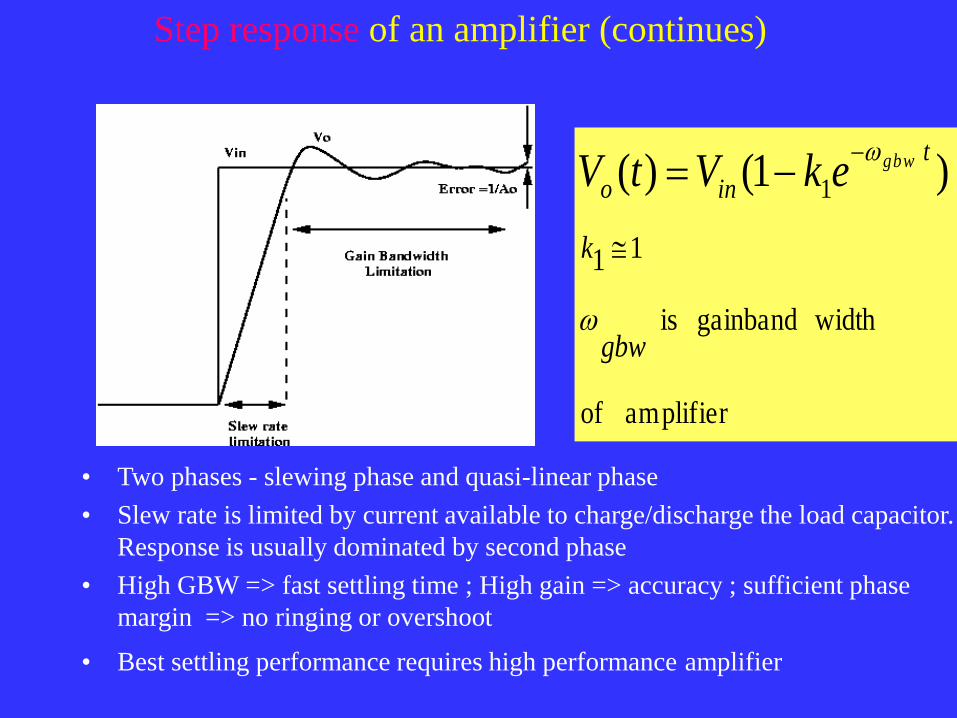
Step response of an amplifier (continues)
• Two phases - slewing phase and quasi-linear phase
• Slew rate is limited by current available to charge/discharge the load capacitor.
Response is usually dominated by second phase
• High GBW => fast settling time ; High gain => accuracy ; sufficient phase
margin => no ringing or overshoot
• Best settling performance requires high performance amplifier
amplifier of
widthgainband is
1 1
)1()(
1
gbw
k
t
inogbwekVtV

• High gain amplifiers => multistage architectures,
low bias currents, large channel lengths
• High bandwidth amplifiers => single stage, high
bias currents, minimum channel lengths
• Difficult to obtain high gain and bandwidth
simultaneously
• Previous architectures settle for an optimal tradeoff
between speed and accuracy requirements
Contradicting requirements for Gain vs Bandwidth ?
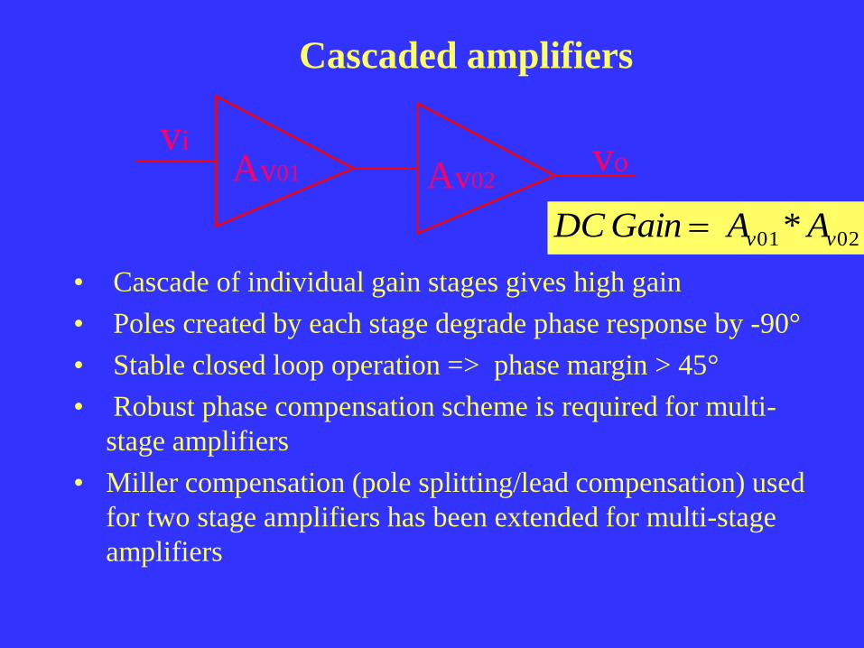
Cascaded amplifiers
• Cascade of individual gain stages gives high gain
• Poles created by each stage degrade phase response by -90°
• Stable closed loop operation => phase margin > 45°
• Robust phase compensation scheme is required for multi-
stage amplifiers
• Miller compensation (pole splitting/lead compensation) used
for two stage amplifiers has been extended for multi-stage
amplifiers
0201 * vv AAGainDC
Av01 Av02
vivo
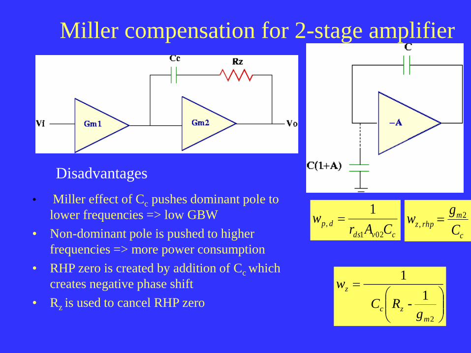
Miller compensation for 2-stage amplifier
• Miller effect of Cc pushes dominant pole to
lower frequencies => low GBW
• Non-dominant pole is pushed to higher
frequencies => more power consumption
• RHP zero is created by addition of Cc which
creates negative phase shift
• Rz is used to cancel RHP zero
cvds
dpCAr
w021
,
1
c
mrhpz
C
gw 2
,
2
1 -
1
m
zc
z
gRC
w
Disadvantages
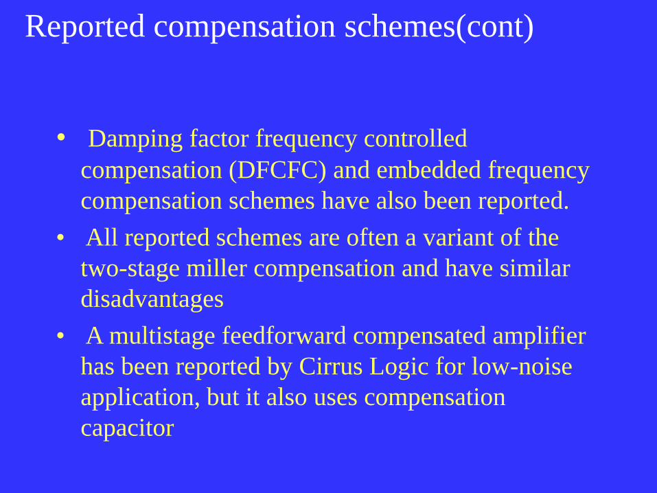
Reported compensation schemes(cont)
• Damping factor frequency controlled
compensation (DFCFC) and embedded frequency
compensation schemes have also been reported.
• All reported schemes are often a variant of the
two-stage miller compensation and have similar
disadvantages
• A multistage feedforward compensated amplifier
has been reported by Cirrus Logic for low-noise
application, but it also uses compensation
capacitor
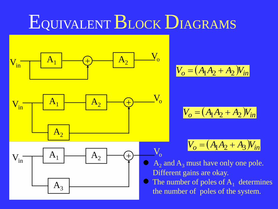
EQUIVALENT BLOCK DIAGRAMS
A1 + A2Vin
Vo
A1 +A2Vin
Vo
A2
A1 +A2Vin
Vo
A3
ino VAAAV 221
ino VAAAV 221
ino VAAAV 321
A2 and A3 must have only one pole.
Different gains are okay.
The number of poles of A1 determines
the number of poles of the system.
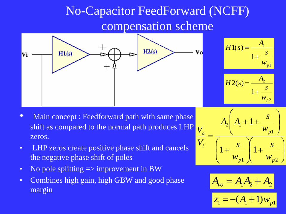
No-Capacitor FeedForward (NCFF)
compensation scheme
• Main concept : Feedforward path with same phase
shift as compared to the normal path produces LHP
zeros.
• LHP zeros create positive phase shift and cancels
the negative phase shift of poles
• No pole splitting => improvement in BW
• Combines high gain, high GBW and good phase
margin
1
1
1
)(1
pw
s
AsH
2
2
1
)(2
pw
s
AsH
21
1
12
11
1
pp
p
i
o
w
s
w
s
w
sAA
V
V
221 AAAAvo
111 )1( pwAz

Miller vs NCFF compensation:Why the difference?

Effect of non-dominant pole
• Number of LHP zeros created is equal to
the order of the first stage
• Main constraint - No non-dominant pole
of second stage before the overall GBW
• For N poles in the system, (N-1) LHP
zeros are created => overall amplifier’s
response is effectively a single pole phase
response
)1)(1(
)(1
,1,1
1
ndpdp w
s
w
s
AsH
2
2
1
)(2
pw
s
AsH
2,1,1
,1,1
12
111
)1)(1(
pndpdp
ndpdp
i
o
w
s
w
s
w
s
w
s
w
sAA
V
V
0 )1)(1(,1,1
12
ndpdp w
s
w
sAA
.
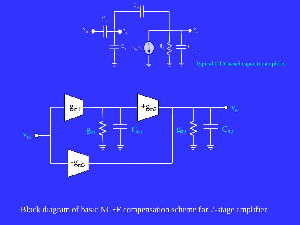
vo
gm
vx
g0 C
4
C2
vin
vx
C1
C3
-gm1 +gm2
-gm3
g01 C01 g02 C02vin
vo
Block diagram of basic NCFF compensation scheme for 2-stage amplifier.
Typical OTA based capacitor amplifier
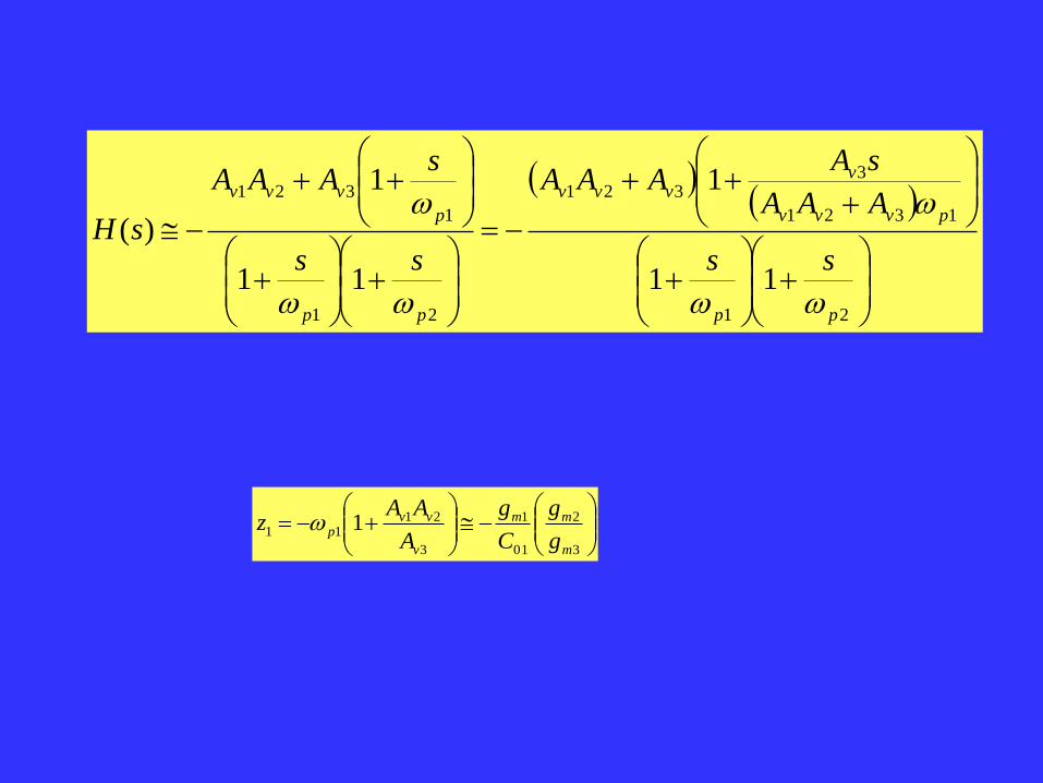
21
1321
3321
21
1
321
11
1
11
1
)(
pp
pvvv
vvvv
pp
p
vvv
ss
AAA
sAAAA
ss
sAAA
sH
3
2
01
1
3
2111 1
m
mm
v
vvp
g
g
C
g
A
AAz
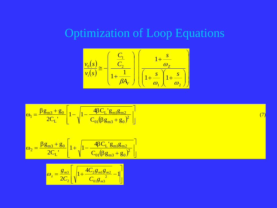
Optimization of Loop Equations
21
2
1
0
11
1
11
ss
s
A
C
C
sv
sv Z
V
i
203m01
2m1mL
L
03m1
ggC
gg'C411
'C2
gg (7)
203m01
2m1mL
L
03m2
ggC
gg'C411
'C2
gg
1
41
22
301
212
2
3
m
mmmz
gC
ggC
C
g
tZtZ
V
i
ee
A
VC
C
tvtv 21
11
1
1
1
11
1
)()(2
2
2
1
1
2
1
000
01
1m
3m
2mz
C
g
g
g (10)
03m01
2m1m1
ggC
gg
(11)
'C
gg
L
03m2
4bCL'gm1gm2/(C01(bgm3+g0)2) < 0.5,
Extending the scheme to multi-stage amplifiers:
Conceptual Representation
• Constraint - Last stage should not have non-
dominant pole before overall GBW
• Number of LHP zeros is one less than the total
number of poles in the system
gm1 gm2
gm2'
vin
vogm3 gm4 gmn
gm3'
gm4'
gmn'
NCFF compensation scheme for
N-Stage Amplifier Implementation

Main features of NCFF compensation
scheme
• Combines high gain and GBW, resulting in a good
settling time and accurate final value
• Good phase margin - when zero exactly cancels the
pole, phase margin is 90°
• No compensation capacitors => lot of reduction in
area, esp for multi-stage amplifiers with 2 or more
compensation capacitors
• Disadvantage - pole-zero mismatch due to process
variations. Pole-zero doublet affects settling time
and phase margin
Effect of pole-zero doublet
• Pole zero doublet causes minor change in
frequency response, but may degrade the settling
time based on their spacing and the zero frequency
• For more accuracy (0.01%), lower frequency
doublet causes more degradation in settling time
because of higher time constant
• For lesser accuracy(0.1%) higher frequency
doublet will cause more degradation because of its
larger amplitude, though it decays faster

Effect of pole-zero mismatch
• Settling time depends on pole-zero
mismatch and zero frequency
• When pole-zero cancellation is at
high frequencies , effect is very
minimal
A) Settling time )1()( 2
21
t
tw
ino ekekVtV g
pole w; zero w
GBW w
1 ;
pz
g
22
zg
pz
ww
wwk
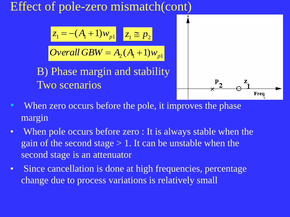
• When zero occurs before the pole, it improves the phase
margin
• When pole occurs before zero : It is always stable when the
gain of the second stage > 1. It can be unstable when the
second stage is an attenuator
• Since cancellation is done at high frequencies, percentage
change due to process variations is relatively small
B) Phase margin and stability
Two scenarios
111 )1( pwAz
112 )1( pwAAGBWOverall
21 pz
Effect of pole-zero mismatch(cont)
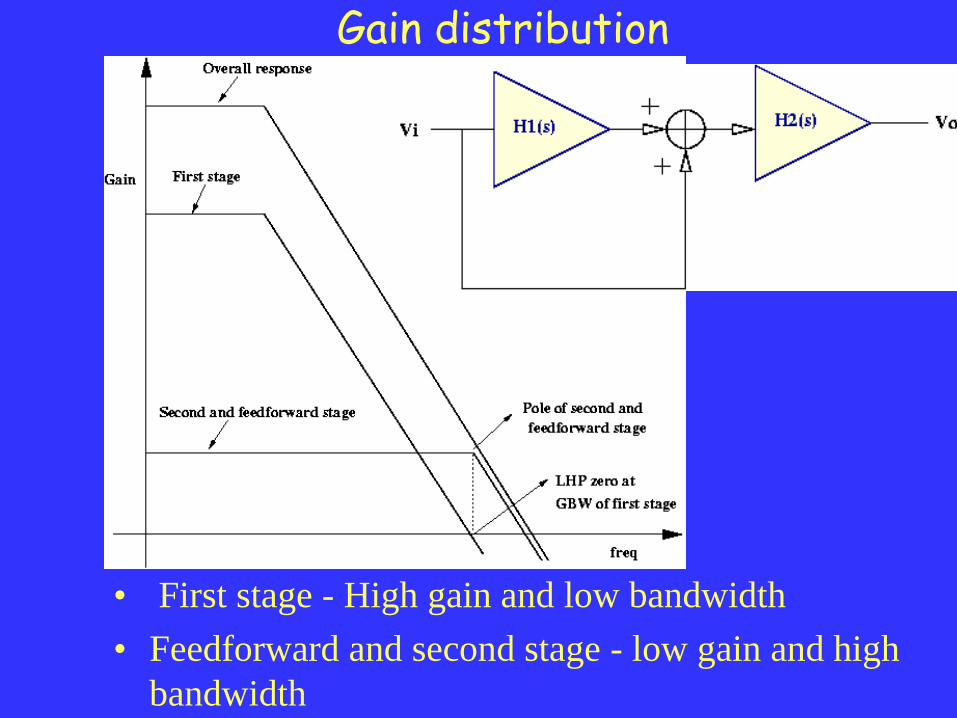
Gain distribution
• First stage - High gain and low bandwidth
• Feedforward and second stage - low gain and high
bandwidth
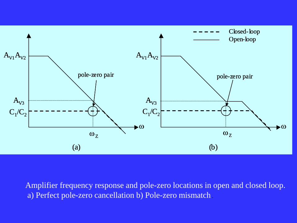
(a) (b)
pole-zero pairpole-zero pair
Closed- loop
Open-loop
AV3
AV1AV2
ZZ
AV3
AV1AV2
C1/C2C1/C2
(a) (b)
pole-zero pairpole-zero pair
Closed- loop
Open-loop
AV3
AV1AV2
ZZ
AV3
AV1AV2
C1/C2C1/C2
Amplifier frequency response and pole-zero locations in open and closed loop.
a) Perfect pole-zero cancellation b) Pole-zero mismatch .

Parasitic capacitance in feedforward path
• Parasitic Cgd capacitance in the feedforward path
exists from input to output node
• When used in closed loop, it is in parallel to
feedback capacitor and attenuates the signal
• Possible solution - use cascode amplifier in the
feedforward stage

Single-ended amplifier (first try)

M1
VSS
VSS
VSS
VDD
VBP
VBN
M1
M4 M4
M5 M5
M6 M6 M7 M7
M2 M2
M3 M3
vi
v0
IB1 IB2
IB3
• •
•
•
• •
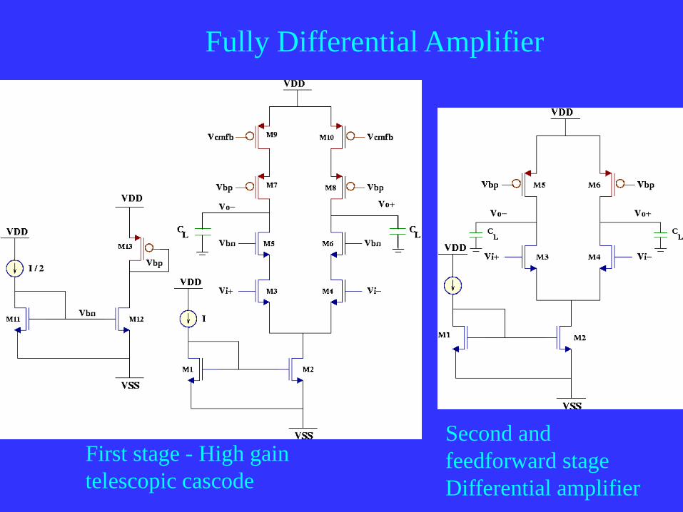
Fully Differential Amplifier
First stage - High gain
telescopic cascode
Second and
feedforward stage
Differential amplifier

Common-mode feedback for first stage
Fully differential amplifier (cont.)

Fully differential amplifier (cont)
19219108m846m6
1||
1
gdvgsdsdsdsds
pCACrrgrrg
19219
41
gdvgs
mz
CAC
g
Ldsdsdsds
pCrrrr 16142022
2||||||
1
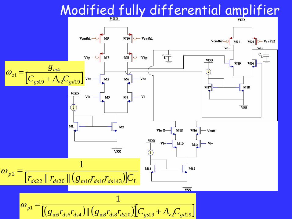
Modified fully differential amplifier
19v219108m846m6
1||
1
gdgsdsdsdsds
pCACrrgrrg
19v219
41
gdgs
mz
CAC
g
Ldsdsmdsds
pCrrgrr 14316162022
2||||
1
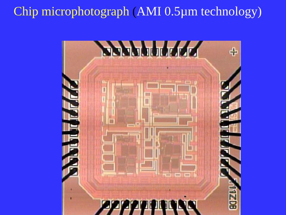
Chip microphotograph (AMI 0.5µm technology)
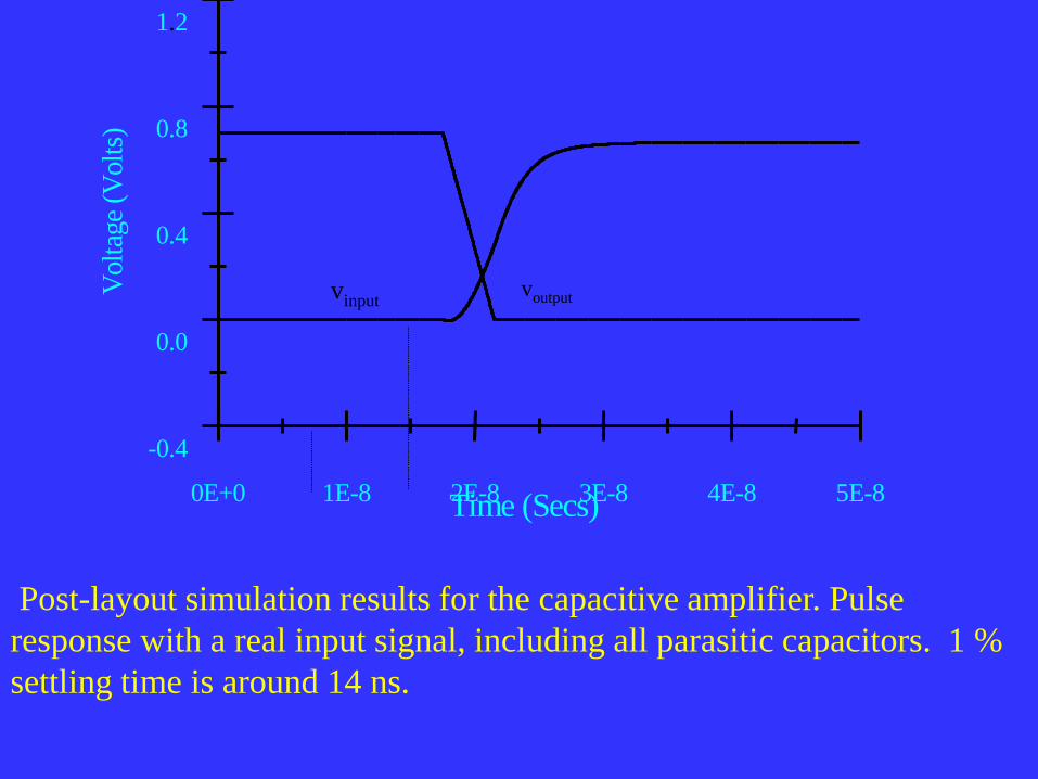
voutputvinput
Post-layout simulation results for the capacitive amplifier. Pulse
response with a real input signal, including all parasitic capacitors. 1 %
settling time is around 14 ns.
0E+0 1E-8 2E-8 3E-8 4E-8 5E-8Time (Secs)
-0.4
0.0
0.4
0.8
1.2
Volt
age
(Volt
s)

Post-layout simulations for OTA’s designed in AMI 0.5µm technology
Parameter Single-ended
OTA
Fully
differential
OTA
DC gain (dB) 94 97
Gainbandwidth (MHz) 300 350
Phase Margin (deg) 74 90
1% settling time (ns) *
6.3 5.1
Current consumption (mA) 5.36 7.16
Power supply 1.25 1.25
Load capacitor = 12 pF
* PCB and probe parasitics not included; ideal step input

0.0E+0 5.0E-9 1.0E-8 1.5E-8 2.0E-8
Time (Secs)
-0.1
0.0
0.1
0.2
0.3
0.4V
olt
age
(Volt
s)
0.25 pF
0.5 pF
1 pF
3 pF7 pF
10 pF
Pulse response post-layout simulation – parametric
sweep of feedback and load capacitors.
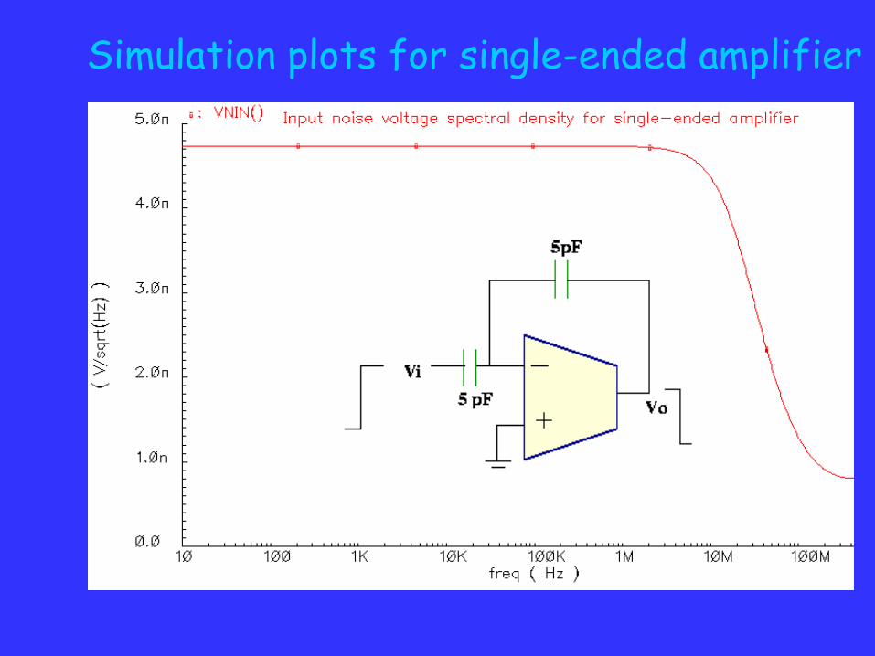
Simulation plots for single-ended amplifier

Simulation plots for differential amplifier
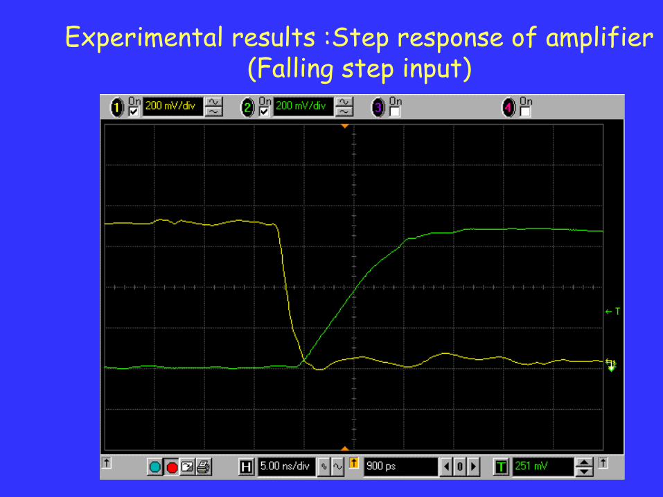
Experimental results :Step response of amplifier (Falling step input)
. Measured pulse response for large input signal.
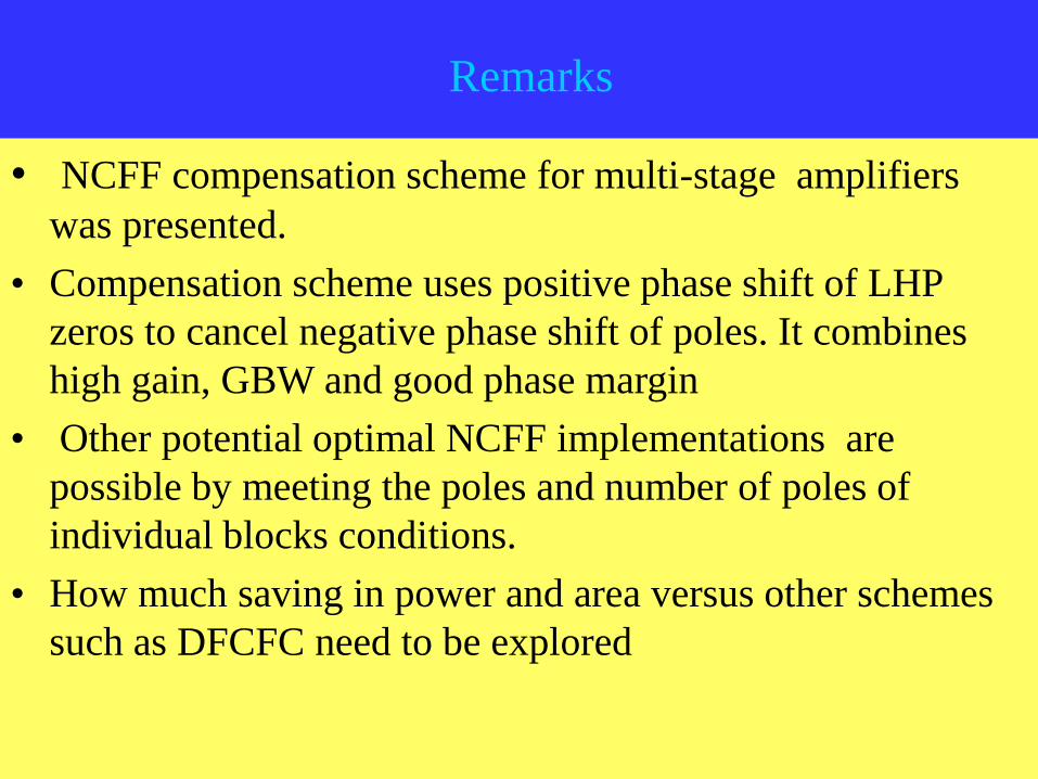
Remarks
• NCFF compensation scheme for multi-stage amplifiers
was presented.
• Compensation scheme uses positive phase shift of LHP
zeros to cancel negative phase shift of poles. It combines
high gain, GBW and good phase margin
• Other potential optimal NCFF implementations are
possible by meeting the poles and number of poles of
individual blocks conditions.
• How much saving in power and area versus other schemes
such as DFCFC need to be explored
A 92 MHz 80 dB peak SNR SC
Bandpass ΣΔ ADC based on NCFF
OTA’s in 0.35µm CMOS technology
Bharath Kumar Thandri and Jose Silva Martinez
AMSC, Texas A&M University
College Station, Texas
Presented at CICC 2003
Reference: A 92MHz, 80dB peak SNR SC bandpass Sigma Delta modulator based on a high GBW OTA with no Miller
capacitors in 0.35 um CMOS technology
Thandri, B.K.; Martinez, J.S.; Rocha-Perez, J.M.; Wang, J.; Custom Integrated Circuits Conference, 2003. Proceedings
of the IEEE 2003 , 21-24 Sept. 2003 Pages:123 - 126
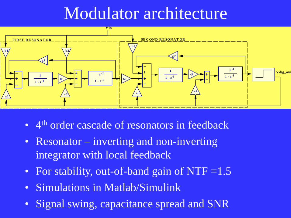
Modulator architecture
• 4th order cascade of resonators in feedback
• Resonator – inverting and non-inverting
integrator with local feedback
• For stability, out-of-band gain of NTF =1.5
• Simulations in Matlab/Simulink
• Signal swing, capacitance spread and SNR
c1
g 1
a 1
-1
SE C ON D R E SON A T OR
Vin
Vdig_out
b3
b2b1
c2
g 2
c3z
1 - z
1
-1
-11 - z-1
z
1 - z
-1
-1
1
1 - z
a 2 a 3a 4
FI R ST R E SON A T OR
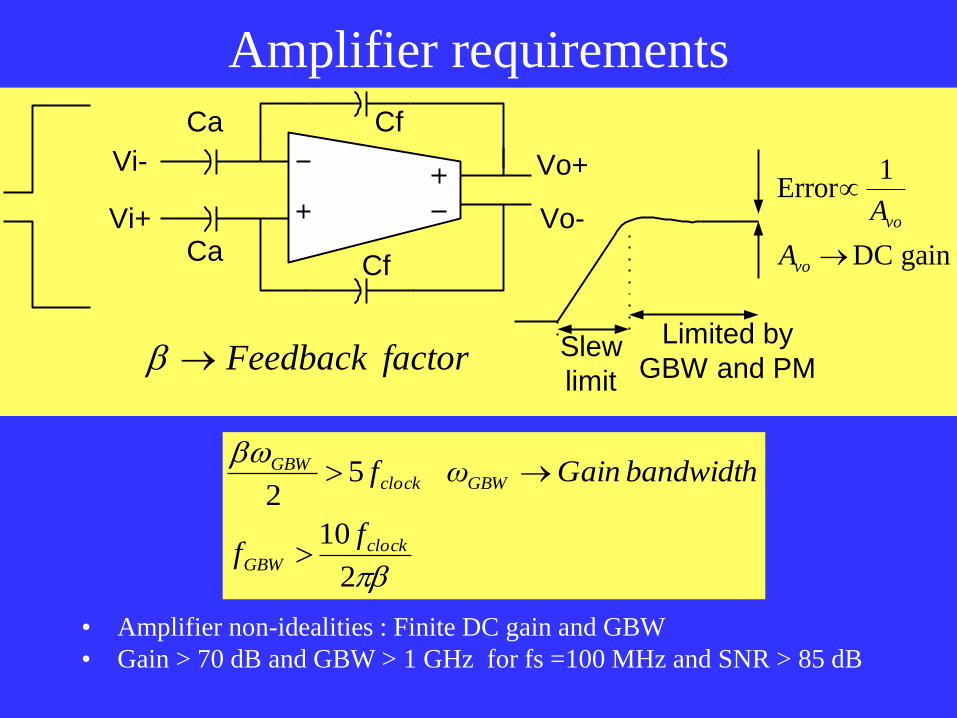
Amplifier requirements
• Amplifier non-idealities : Finite DC gain and GBW
• Gain > 70 dB and GBW > 1 GHz for fs =100 MHz and SNR > 85 dB
2
10
5 2
clockGBW
GBWclockGBW
ff
bandwidthGain ωf
Ca Cf
CfCa
Vo-
Vo+
Vi+
Vi-
gain DC
1Error
vo
vo
A
A
Limited by
GBW and PMSlew
limitfactorFeedback
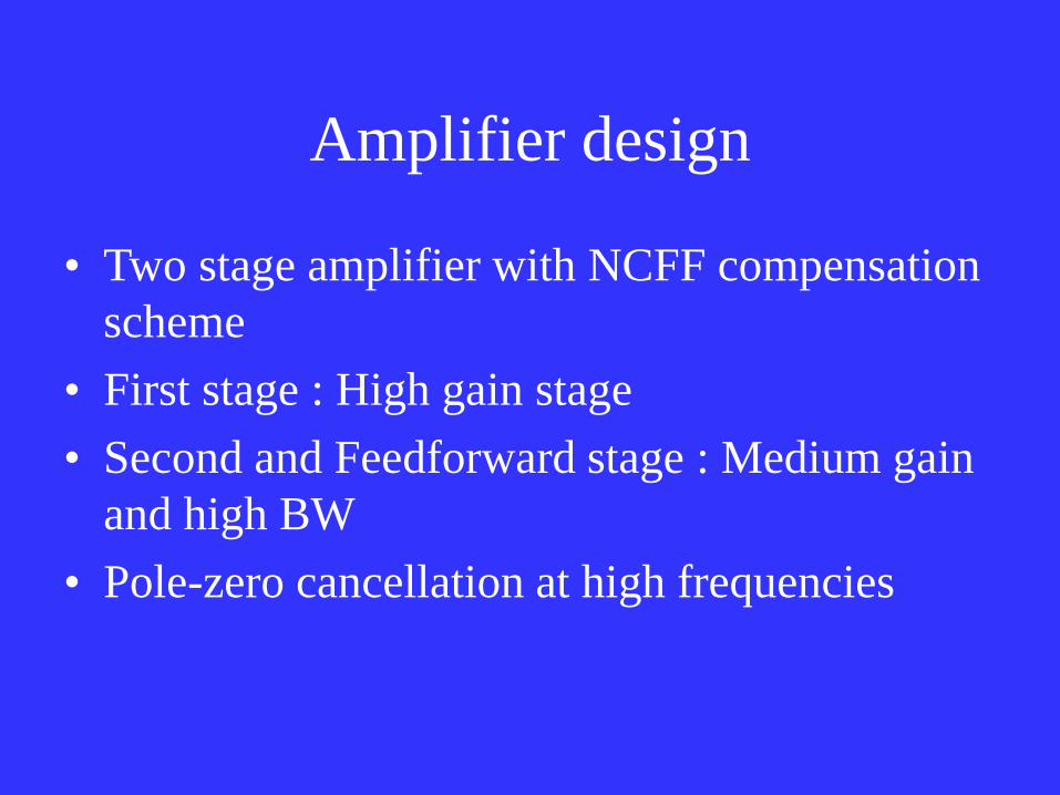
Amplifier design
• Two stage amplifier with NCFF compensation
scheme
• First stage : High gain stage
• Second and Feedforward stage : Medium gain
and high BW
• Pole-zero cancellation at high frequencies

Amplifier (final version)
• Use cascode in FF stage
• Conventional CMFB for both
stages
• CMFB capacitors increase
loading at output
• Bias network to fix Vg of
M2,M3 and M6
• Currents
First stage = 100 μA
Second stage = 1.25 mA
FF stage = 3.25 mA
VDD VDD
VSS
VSS
VSS
Vi+ Vi-
Vi+ Vi-
Vo- Vo+
Vbn1 Vbn1
Vbp Vbp
Vcmfb1 Vcmfb1Vcmfb2
Vcmfb2
M2M2
M3M3
M4M4
M5M5
M7M7
M8M8
M1M1
M6M6Vbn2 Vbn2
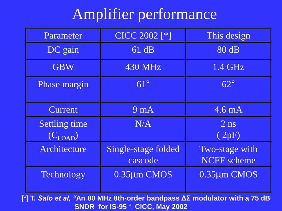
Amplifier performance
Parameter CICC 2002 [*] This design
DC gain 61 dB 80 dB
GBW 430 MHz 1.4 GHz
Phase margin 61° 62°
Current 9 mA 4.6 mA
Settling time
(CLOAD)
N/A 2 ns
( 2pF)
Architecture Single-stage folded
cascode
Two-stage with
NCFF scheme
Technology 0.35µm CMOS 0.35µm CMOS
[*] T. Salo et al, “An 80 MHz 8th-order bandpass ΔΣ modulator with a 75 dB
SNDR for IS-95 “, CICC, May 2002
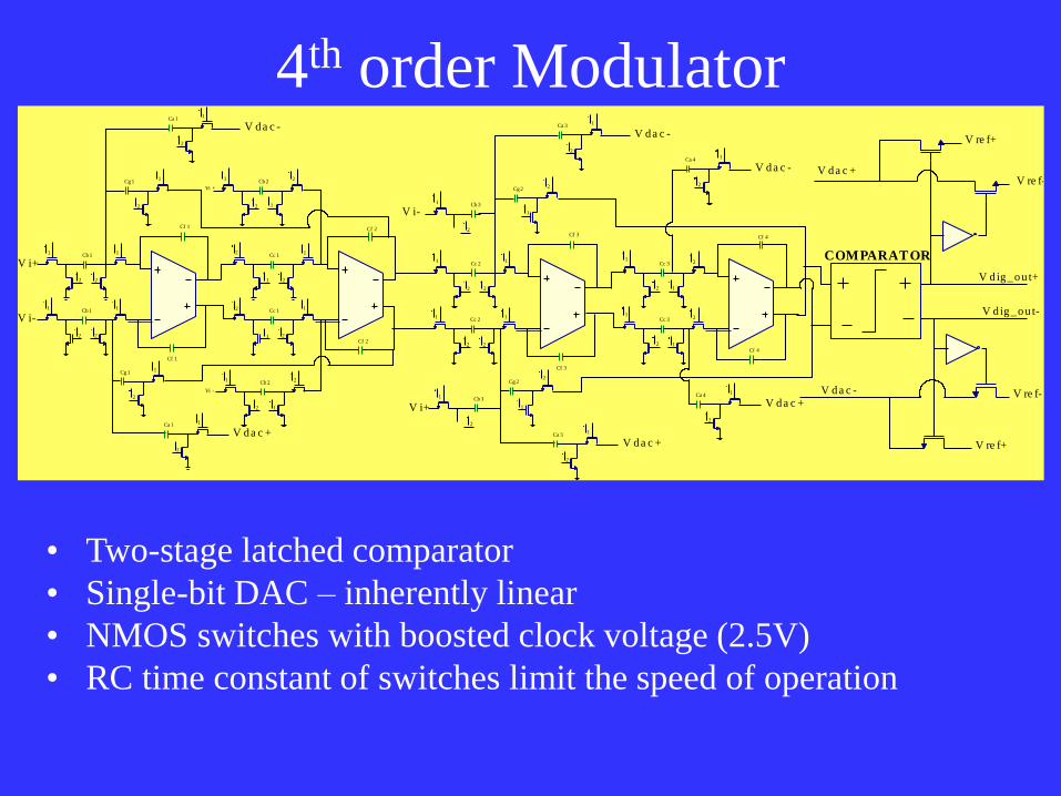
4th order Modulator
• Two-stage latched comparator
• Single-bit DAC – inherently linear
• NMOS switches with boosted clock voltage (2.5V)
• RC time constant of switches limit the speed of operation
2
1
2
1
1
1
2
1
2
1
2
2
2
2
2
1
2
1
2
1
2
1
2 2
1 1
2 2
1
1
1
1
2
1
2 2
1 1
2
1
2
1
2
1
1
2
2
1
1
2
2
1
1
2
2
1
2
1
2
1
2
1
2
1
Cf 1
Cc 1
Cb 2
Cb 2
Cf 2
V da c +
V da c -
Vi -
Vi +
Cf 2
Cg 1
Ca 1
Cg 1
Ca 1
Cb 1
Cb 1
Cf 1
Cc 1
Cf 3
Cc 3
Cf 4
V da c -
Cf 4
Ca 3
Cc 2
Cf 3
Cc 2
Cb 3
V da c -
Cb 3
Cc 3
Ca 4
Ca 4
Cg 2
Cg 2
V da c +Ca 3
COMPARATOR
V da c +
V da c +
V da c -
V re f-
V re f+
V dig_ou t+
V dig_ou t-
V re f-
V re f+
V i-
V i+
V i-
V i+
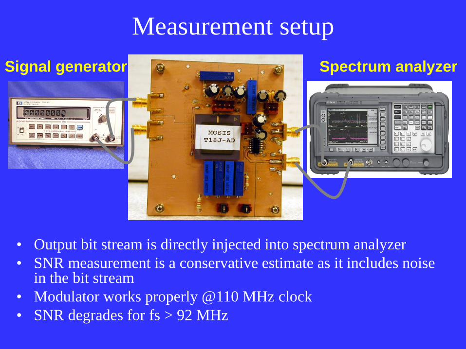
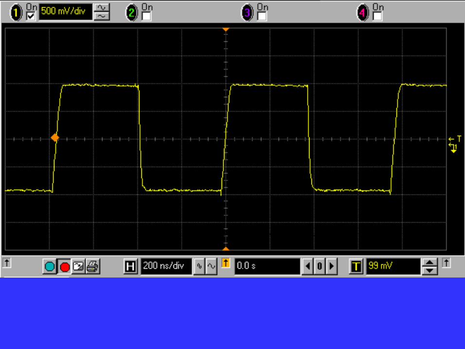
Measurement setup
• Output bit stream is directly injected into spectrum analyzer
• SNR measurement is a conservative estimate as it includes noise in the bit stream
• Modulator works properly @110 MHz clock
• SNR degrades for fs > 92 MHz
Signal generator Spectrum analyzer
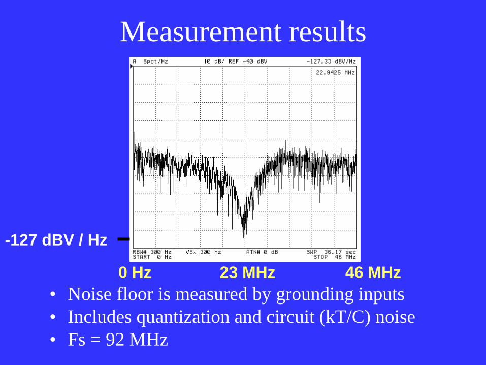
Measurement results
• Noise floor is measured by grounding inputs
• Includes quantization and circuit (kT/C) noise
• Fs = 92 MHz
-127 dBV / Hz
0 Hz 46 MHz23 MHz
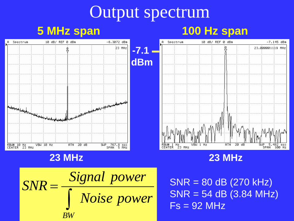
Output spectrum
powerNoise
powerSignalSNR
BW
5 MHz span 100 Hz span
SNR = 80 dB (270 kHz)
SNR = 54 dB (3.84 MHz)
Fs = 92 MHz
23 MHz 23 MHz
-7.1
dBm

Two tone IMD test
• Two tone input @ -11 dBr, 23.1 and 22.9 MHz
• Measured IMD3 = -58 dB
-70 dBm
-12 dBm
22.9 MHz 23.1 MHz
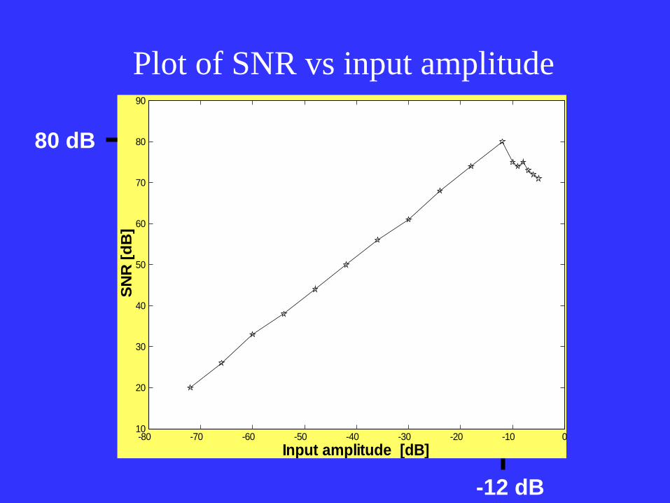
Plot of SNR vs input amplitude
-80 -70 -60 -50 -40 -30 -20 -10 010
20
30
40
50
60
70
80
90
Input amplitude [dB]
SN
R [
dB
]80 dB
-12 dB

Performance summary of the modulator
Technology TSMC 0.35μm
CMOS
Peak SNR for 270 KHz BW 80 dB
Peak SNR for 3.84 MHz BW 54 dB
IMD3 @ -11dBr input -58 dB
Supply voltage ±1.25V
Power consumption 47.5 mW
Sampling frequency 92 MHz
Core area 1.248 mm2
References
S. Pernici, “A CMOS Low-Distortion Fully Differential Power Amplifier with Double Nested
Miller Compensation,” IEEE J. Solid-State Circuits, Vol. 28, No. 7, pp. 758-763, July 1993.
F. You, S.H.K. Embabi and E. Sánchez-Sinencio, “Multistage Amplifier Topologies with
Nested Gm-C Compensation,” IEEE J. of Solid-State Circuits, Vol. 32, No. 12, pp. 2000-2011,
December 1997.
X. Xie, M.C. Schneider, E. Sánchez-Sinencio and S.H.K. Embabi, “ Sound Design of low power nested
transconconductance-capacitance compensation amplifiers” Electronics Letters, Vol. 35, No. 12, pp956-
958, June 1999
K.N. Leung, P.K. T. Mok, W.-H. Ki, and J. K. O. Sin, “ Three-Stage Large Capacitive Load
Amplifier with Damping Factor-Control Frequency Compensation, “IEEE J. of Solid-State
Circuits, Vol. 35, No. 2, pp. 221-230, February 2000
B.K. Thandri, , and J. Silva-Martinez, “ A Feedforward Compensation Scheme for Multi-Stage Amplifiers
with No-Miller Capacitors”, IEEE J. Solid State Circuits, Vol. 38, pp. 237-243, Feb. 2003.
X. Fan, C. Mishra and E. Sánchez-Sinencio, “Single Miller Capacitor Frequency
Compensation Technique for Low Power Multistage Amplifiers,” IEEE Journal of Solid-State
Circuits, Vol. 40, No. 3, March 2005.
Analog & Mixed-Signal Center (AMSC)


