1 DATASHEET Low Power RTC with Battery Backed SRAM, Integrated ±5ppm Temperature Compensation and Auto Daylight Saving ISL12020M The ISL12020M device is a low power Real Time Clock (RTC) with an embedded temperature sensor and crystal. Device functions include oscillator compensation, clock/calendar, power fail and low battery monitors, brownout indicator, one-time, periodic or polled alarms, intelligent battery backup switching, Battery Reseal™ function and 128 bytes of battery-backed user SRAM. The device is offered in a 20 Ld DFN module that contains the RTC and an embedded 32.768kHz quartz crystal. The calibrated oscillator provides less than ±5ppm drift across the 0°C to +85°C temperature range. The RTC tracks time with separate registers for hours, minutes and seconds. The calendar registers track date, month, year and day of the week and are accurate through 2099, with automatic leap year correction. Daylight Savings time adjustment is done automatically, using parameters entered by the user. Power fail and battery monitors offer user-selectable trip levels. The time stamp function records the time and date of switchover from V DD to V BAT power and also from V BAT to V DD power. Related Literature • AN1549 , “Addressing Power Issues in Real Time Clock Applications” • AN1389 , “Using Intersil’s High Accuracy Real Time Clock Module” Features • Embedded 32.768kHz quartz crystal in the package • 20 Ld DFN package (for SOIC version, refer to the ISL12022M) • Calendar • On-chip oscillator temperature compensation • 10-bit digital temperature sensor output • 15 selectable frequency outputs • Interrupt for alarm or 15 selectable frequency outputs • Automatic backup to battery or supercapacitor •V DD and battery status monitors • Battery Reseal™ function to extend battery shelf life • Power status brownout monitor • Time stamp for battery switchover • 128 Bytes battery-backed user SRAM •I 2 C-Bus™ • RoHS compliant Applications • Utility meters • POS equipment • Printers and copiers • Digital cameras ISL12020M 3.3V C1 0.1µF BAT54 SDA SCL GND VDD BATTERY 3.0V C2 0.1µF SCHOTTKY DIODE 1 2 3 4 5 6 7 8 9 10 X2 X2 X2 X2 X2 NC VBAT GND NC NC 11 12 13 14 15 16 17 18 19 20 SDA SCL VDD NC X1 X1 X1 X1 X1 10k R2 10k R3 10k IRQ/FOUT IRQ/FOUT MCU INTERFACE R1 FIGURE 1. TYPICAL APPLICATION CIRCUIT CAUTION: These devices are sensitive to electrostatic discharge; follow proper IC Handling Procedures. 1-888-INTERSIL or 1-888-468-3774 | Copyright Intersil Americas LLC 2008-2011, 2015. All Rights Reserved Intersil (and design) is a trademark owned by Intersil Corporation or one of its subsidiaries. I 2 C Bus™ is a trademark owned by NXP Semiconductors Netherlands, B.V. All other trademarks mentioned are the property of their respective owners. January 9, 2015 FN6667.6
Transcript
DATASHEET
Low Power RTC with Battery Backed SRAM, Integrated ±5ppm Temperature Compensation and Auto Daylight SavingISL12020MThe ISL12020M device is a low power Real Time Clock (RTC) with an embedded temperature sensor and crystal. Device functions include oscillator compensation, clock/calendar, power fail and low battery monitors, brownout indicator, one-time, periodic or polled alarms, intelligent battery backup switching, Battery Reseal™ function and 128 bytes of battery-backed user SRAM. The device is offered in a 20 Ld DFN module that contains the RTC and an embedded 32.768kHz quartz crystal. The calibrated oscillator provides less than ±5ppm drift across the 0°C to +85°C temperature range.
The RTC tracks time with separate registers for hours, minutes and seconds. The calendar registers track date, month, year and day of the week and are accurate through 2099, with automatic leap year correction.
Daylight Savings time adjustment is done automatically, using parameters entered by the user. Power fail and battery monitors offer user-selectable trip levels. The time stamp function records the time and date of switchover from VDD to VBAT power and also from VBAT to VDD power.
Related Literature• AN1549, “Addressing Power Issues in Real Time Clock
Applications”
• AN1389, “Using Intersil’s High Accuracy Real Time Clock Module”
Features• Embedded 32.768kHz quartz crystal in the package
• 20 Ld DFN package (for SOIC version, refer to the ISL12022M)
• Calendar
• On-chip oscillator temperature compensation
• 10-bit digital temperature sensor output
• 15 selectable frequency outputs
• Interrupt for alarm or 15 selectable frequency outputs
• Automatic backup to battery or supercapacitor
• VDD and battery status monitors
• Battery Reseal™ function to extend battery shelf life
• Power status brownout monitor
• Time stamp for battery switchover
• 128 Bytes battery-backed user SRAM
• I2C-Bus™
• RoHS compliant
Applications• Utility meters
• POS equipment
• Printers and copiers
• Digital cameras
ISL12020M
3.3V
C1
0.1µFBAT54
SDA
SCL
GND
VDDBATTERY
3.0VC2
0.1µF
SCHOTTKY DIODE
1
2
3
4
5
6
7
8
9
10
X2
X2
X2
X2
X2
NC
VBAT
GND
NC
NC 11
12
13
14
15
16
17
18
19
20
SDA
SCL
VDD
NC
X1
X1
X1
X1
X1
10k
R2
10k
R3
10kIRQ/FOUT
IRQ/FOUT
MCU INTERFACE
R1
FIGURE 1. TYPICAL APPLICATION CIRCUIT
1 CAUTION: These devices are sensitive to electrostatic discharge; follow proper IC Handling Procedures.1-888-INTERSIL or 1-888-468-3774 |Copyright Intersil Americas LLC 2008-2011, 2015. All Rights Reserved
Intersil (and design) is a trademark owned by Intersil Corporation or one of its subsidiaries. I2C Bus™ is a trademark owned byNXP Semiconductors Netherlands, B.V. All other trademarks mentioned are the property of their respective owners.
ISL12020MIRZ ISL 12020MIRZ 2.7 to 5.5 -40 to +85 20 Ld DFN L20.5.5x4.0
ISL12020MIRZ-EVALZ Evaluation Board
NOTES:
1. Add “-T*” suffix for tape and reel. Please refer to TB347 for details on reel specifications.
2. These Intersil Pb-free plastic packaged products employ special Pb-free material sets, molding compounds/die attach materials and 100% matte tin plate plus anneal (e3 termination finish, which is RoHS compliant and compatible with both SnPb and Pb-free soldering operations). Intersil Pb-free products are MSL classified at Pb-free peak reflow temperatures that meet or exceed the Pb-free requirements of IPC/JEDEC J STD-020.
3. For Moisture Sensitivity Level (MSL), please see device information page for ISL12020M. For more information on MSL please see techbrief TB363.
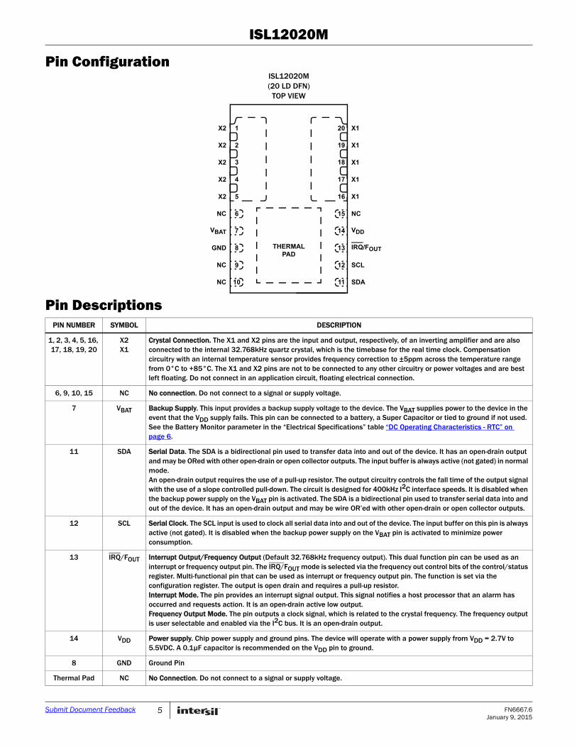
Crystal Connection. The X1 and X2 pins are the input and output, respectively, of an inverting amplifier and are also connected to the internal 32.768kHz quartz crystal, which is the timebase for the real time clock. Compensation circuitry with an internal temperature sensor provides frequency correction to ±5ppm across the temperature range from 0°C to +85°C. The X1 and X2 pins are not to be connected to any other circuitry or power voltages and are best left floating. Do not connect in an application circuit, floating electrical connection.
6, 9, 10, 15 NC No connection. Do not connect to a signal or supply voltage.
7 VBAT Backup Supply. This input provides a backup supply voltage to the device. The VBAT supplies power to the device in the event that the VDD supply fails. This pin can be connected to a battery, a Super Capacitor or tied to ground if not used. See the Battery Monitor parameter in the “Electrical Specifications” table “DC Operating Characteristics - RTC” on page 6.
11 SDA Serial Data. The SDA is a bidirectional pin used to transfer data into and out of the device. It has an open-drain output and may be ORed with other open-drain or open collector outputs. The input buffer is always active (not gated) in normal mode.An open-drain output requires the use of a pull-up resistor. The output circuitry controls the fall time of the output signal with the use of a slope controlled pull-down. The circuit is designed for 400kHz I2C interface speeds. It is disabled when the backup power supply on the VBAT pin is activated. The SDA is a bidirectional pin used to transfer serial data into and out of the device. It has an open-drain output and may be wire OR’ed with other open-drain or open collector outputs.
12 SCL Serial Clock. The SCL input is used to clock all serial data into and out of the device. The input buffer on this pin is always active (not gated). It is disabled when the backup power supply on the VBAT pin is activated to minimize power consumption.
13 IRQ/FOUT Interrupt Output/Frequency Output (Default 32.768kHz frequency output). This dual function pin can be used as an interrupt or frequency output pin. The IRQ/FOUT mode is selected via the frequency out control bits of the control/status register. Multi-functional pin that can be used as interrupt or frequency output pin. The function is set via the configuration register. The output is open drain and requires a pull-up resistor.Interrupt Mode. The pin provides an interrupt signal output. This signal notifies a host processor that an alarm has occurred and requests action. It is an open-drain active low output.Frequency Output Mode. The pin outputs a clock signal, which is related to the crystal frequency. The frequency output is user selectable and enabled via the I2C bus. It is an open-drain output.
14 VDD Power supply. Chip power supply and ground pins. The device will operate with a power supply from VDD = 2.7V to 5.5VDC. A 0.1µF capacitor is recommended on the VDD pin to ground.
8 GND Ground Pin
Thermal Pad NC No Connection. Do not connect to a signal or supply voltage.
CAUTION: Do not operate at or near the maximum ratings listed for extended periods of time. Exposure to such conditions may adversely impact productreliability and result in failures not covered by warranty.
NOTES:
4. JA is measured in free air with the component mounted on a high effective thermal conductivity test board with “direct attach” features. See Tech Brief TB379.
5. For JC, the “case temp” location is the center of the exposed metal pad on the package underside.
6. The X1 and X2 pins are connected internally to a crystal and should be a floating electrical connection.
7. The ISL12020M Oscillator Initial Accuracy can change after solder reflow attachment. The amount of change will depend on the reflow temperature and length of exposure. A general rule is to use only one reflow cycle and keep the temperature and time as short as possible. Changes on the order of ±1ppm to ±3ppm can be expected with typical reflow profiles.
DC Operating Characteristics - RTC Test Conditions: VDD = +2.7 to +5.5V, TA = -40°C to +85°C, unless otherwise stated. Boldface limits apply across the operating temperature range, -40°C to +85°C.
SYMBOL PARAMETER CONDITIONSMIN
(Note 8)TYP
(Note 9)MAX
(Note 8) UNITS NOTES
VDD Main Power Supply (Note 10) 2.7 5.5 V
VBAT Battery Supply Voltage (Note 10) 1.8 5.5 V 11
IDD1 Supply Current. (I2C not active, temperature conversion not active, FOUT not active)
VDD = 5V 4.1 15 µA 12, 13
VDD = 3V 3.5 14 µA 12, 13
IDD2 Supply Current. (I2C Active, Temperature Conversion not Active, FOUT not Active)
VDD = 5V 200 500 µA 12, 13
IDD3 Supply Current. (I2C not Active, Temperature Conversion Active, FOUT not Active)
VDD = 5V 120 400 µA 12, 13
IBAT Battery Supply Current VDD = 0V, VBAT = 3V, TA = +25°C 1.0 1.6 µA 12
FoutT Oscillator Stability vs Temperature VDD = 3.3V, 0°C to +85°C -5 +5 ppm 7, 15
VDD = 3.3V, -30°C to +85°C -10 +10 ppm 7, 15
VDD = 3.3V, -40°C to +85°C -15 +15 ppm 7, 15
FoutV Oscillator Stability vs Voltage 2.7V VDD 5.5V -3 +3 ppm 15
Temperature Sensor Accuracy VDD = VBAT = 3.3V ±2 °C 15
IRQ/FOUT (OPEN-DRAIN OUTPUT)
VOL Output Low Voltage VDD = 5V, IOL = 3mA 0.4 V
VDD = 2.7V, IOL = 1mA 0.4 V
DC Operating Characteristics - RTC Test Conditions: VDD = +2.7 to +5.5V, TA = -40°C to +85°C, unless otherwise stated. Boldface limits apply across the operating temperature range, -40°C to +85°C. (Continued)
SYMBOL PARAMETER CONDITIONSMIN
(Note 8)TYP
(Note 9)MAX
(Note 8) UNITS NOTES
Power-Down Timing Test Conditions: VDD = +2.7 to +5.5V, Temperature = -40°C to +85°C, unless otherwise stated. Boldface limits apply across the operating temperature range, -40°C to +85°C.
I2C Interface Specifications Test Conditions: VDD = +2.7 to +5.5V, Temperature = -40°C to +85°C, unless otherwise specified. Boldface limits apply across the operating temperature range, -40°C to +85°C.
SYMBOL PARAMETER TEST CONDITIONSMIN
(Note 8)TYP
(Note 9)MAX
(Note 8) UNITS NOTES
VIL SDA and SCL Input Buffer LOW Voltage
-0.3 0.3 x VDD V
VIH SDA and SCL Input Buffer HIGH Voltage
0.7 x VDD VDD + 0.3 V
Hysteresis SDA and SCL Input Buffer Hysteresis
0.05 x VDD V 15, 16
VOL SDA Output Buffer LOW Voltage, Sinking 3mA
VDD = 5V, IOL = 3mA 0 0.02 0.4 V
CPIN SDA and SCL Pin Capacitance TA = +25°C, f = 1MHz, VDD = 5V, VIN = 0V, VOUT = 0V
10 pF 15, 16
fSCL SCL Frequency 400 kHz
tIN Pulse Width Suppression Time at SDA and SCL Inputs
Any pulse narrower than the max spec is suppressed.
50 ns
tAA SCL Falling Edge to SDA Output Data Valid
SCL falling edge crossing 30% of VDD, until SDA exits the 30% to 70% of VDD window.
900 ns
tBUF Time the Bus Must be Free Before the Start of a New Transmission
SDA crossing 70% of VDD during a STOP condition, to SDA crossing 70% of VDD during the following START condition.
1300 ns
tLOW Clock LOW Time Measured at the 30% of VDD crossing.
tHIGH Clock HIGH Time Measured at the 70% of VDD crossing.
600 ns
tSU:STA START Condition Setup Time SCL rising edge to SDA falling edge. Both crossing 70% of VDD.
600 ns
tHD:STA START Condition Hold Time From SDA falling edge crossing 30% of VDD to SCL falling edge crossing 70% of VDD.
600 ns
tSU:DAT Input Data Setup Time From SDA exiting the 30% to 70% of VDD window, to SCL rising edge crossing 30% of VDD.
100 ns
tHD:DAT Input Data Hold Time From SCL falling edge crossing 30% of VDD to SDA entering the 30% to 70% of VDD window.
20 900 ns
tSU:STO STOP Condition Setup Time From SCL rising edge crossing 70% of VDD, to SDA rising edge crossing 30% of VDD.
600 ns
tHD:STO STOP Condition Hold Time From SDA rising edge to SCL falling edge. Both crossing 70% of VDD.
600 ns
tDH Output Data Hold Time From SCL falling edge crossing 30% of VDD, until SDA enters the 30% to 70% of VDD window.
0 ns
tR SDA and SCL Rise Time From 30% to 70% of VDD. 20 + 0.1 x Cb
300 ns 16
tF SDA and SCL Fall Time From 70% to 30% of VDD. 20 + 0.1 x Cb
300 ns 16
Cb Capacitive Loading of SDA or SCL Total on-chip and off-chip 10 400 pF 16
RPU SDA and SCL Bus Pull-up Resistor Off-chip
Maximum is determined by tR and tF. For Cb = 400pF, max is about 2kΩ~2.5kΩ.For Cb = 40pF, max is about 15kΩ~20kΩ
1 kΩ 16
NOTES:
8. Parameters with MIN and/or MAX limits are 100% tested at +25°C, unless otherwise specified. Temperature limits established by characterization and are not production tested.
9. Specified at +25°C.
10. Minimum VDD and/or VBAT of 1V to sustain the SRAM. The value is based on characterization and it is not tested.
11. Temperature Conversion is inactive below VBAT = 2.7V. Device operation is not guaranteed at VBAT<1.8V.
12. IRQ/FOUT Inactive.
13. VDD > VBAT +VBATHYS14. In order to ensure proper timekeeping, the VDD SR- specification must be followed.
15. Limits should be considered typical and are not production tested.
16. These are I2C specific parameters and are not tested, however, they are used to set conditions for testing devices to validate specification.
17. To avoid EEPROM recall issues, it is advised to use this minimum power up slew rate. Not tested, shown as typical only.
I2C Interface Specifications Test Conditions: VDD = +2.7 to +5.5V, Temperature = -40°C to +85°C, unless otherwise specified. Boldface limits apply across the operating temperature range, -40°C to +85°C. (Continued)
General DescriptionThe ISL12020M device is a low power Real Time Clock (RTC) with embedded temperature sensor and crystal. It contains crystal frequency compensation circuitry over the temperature range of 0°C to 85°C good to ±5ppm accuracy. It also contains a clock/calendar with Daylight Savings Time (DST) adjustment, power fail and low battery monitors, brownout indicator, 1 periodic or polled alarm, intelligent battery-backup switching and 128 Bytes of battery-backed user SRAM.
The oscillator uses an internal 32.768kHz crystal. The real time clock tracks time with separate registers for hours, minutes and seconds. The device has calendar registers for date, month, year and day of the week. The calendar is accurate through 2099, with automatic leap year correction. In addition, both the ISL12020M could be programmed for automatic Daylight Savings Time (DST) adjustment by entering local DST information.
The ISL12020M’s alarm can be set to any clock/calendar value for a match. For example, every minute, every Tuesday or at 5:23 AM on March 21. The alarm status is available by checking the Status Register, or the device can be configured to provide a hardware interrupt via the IRQ/FOUT pin. There is a repeat mode for the alarm allowing a periodic interrupt every minute, every hour, every day, etc.
The device also offers a backup power input pin. This VBAT pin allows the device to be backed up by battery or Super Capacitor with automatic switchover from VDD to VBAT. The ISL12020M device is specified for VDD = 2.7V to 5.5V and the clock/calendar portion of the device remains fully operational in battery-backup mode down to 1.8V (Standby Mode). The VBAT level is monitored and reported against preselected levels. The first report is registered when the VBAT level falls below 85% of nominal level, the second level is set for 75%. Battery levels are stored in PWR_VBAT registers.
The ISL12020M offers a “Brownout” alarm once the VDD falls below a preselected trip level. This allows system Micro to save vital information to memory before complete power loss. There are six VDD levels that could be selected for initiation of the Brownout alarm.
Functional DescriptionPower Control OperationThe power control circuit accepts a VDD and a VBAT input. Many types of batteries can be used with Intersil RTC products. For example, 3.0V or 3.6V Lithium batteries are appropriate and battery sizes are available that can power the ISL12020M for up to 10 years. Another option is to use a Super Capacitor for applications where VDD is interrupted for up to a month. See the “Application Section” on page 28 for more information.
Normal Mode (VDD) to Battery-Backup Mode (VBAT)To transition from the VDD to VBAT mode, both of the following conditions must be met:
Condition 1:
VDD < VBAT - VBATHYSwhere VBATHYS 50mV
Condition 2:
VDD < VTRIP where VTRIP 2.2V
Battery-Backup Mode (VBAT) to Normal Mode (VDD)The ISL12020M device will switch from the VBAT to VDD mode when one of the following conditions occurs:
Condition 1:
VDD > VBAT + VBATHYSwhere VBATHYS 50mV
Condition 2:
VDD > VTRIP + VTRIPHYSwhere VTRIPHYS 30mV
These power control situations are illustrated in Figures 13 and 14.
FIGURE 11. IDD with TSE = 1 vs TEMPERATURE FIGURE 12. OSCILLATOR CHANGE vs TEMPERATURE AT DIFFERENT AGING SETTINGS (IATR) (BETA SET FOR 1ppm STEPS)
Typical Performance Curves Temperature is +25°C unless otherwise specified. (Continued)
The I2C bus is deactivated in battery-backup mode to reduce power consumption. Aside from this, all RTC functions are operational during battery-backup mode. Except for SCL and SDA, all the inputs and outputs of the ISL12020M are active during battery-backup mode unless disabled via the control register.
The device Time Stamps the switchover from VDD to VBAT and VBAT to VDD and the time is stored in tSV2B and tSB2V registers respectively. If multiple VDD power-down sequences occur before status is read, the earliest VDD to VBAT power-down time is stored and the most recent VBAT to VDD time is stored.
Temperature conversion and compensation can be enabled in battery-backup mode. Bit BTSE in the BETA register controls this operation, as described in “BETA Register (BETA)” on page 20.
Power Failure DetectionThe ISL12020M provides a Real Time Clock Failure Bit (RTCF) to detect total power failure. It allows users to determine if the device has powered up after having lost all power to the device (both VDD and VBAT).
Brownout DetectionThe ISL12020M monitors the VDD level continuously and provides warning if the VDD level drops below prescribed levels. There are six (6) levels that can be selected for the trip level. These values are 85% below popular VDD levels. The LVDD bit in the Status Register will be set to “1” when brownout is detected. Note that the I2C serial bus remains active unless the Battery VTRIP levels are reached.
Battery Level MonitorThe ISL12020M has a built in warning feature once the Back Up battery level drops first to 85% and then to 75% of the battery’s nominal VBAT level. When the battery voltage drops to between
85% and 75%, the LBAT85 bit is set in the status register. When the level drops below 75%, both LBAT85 and LBAT75 bits are set in the status register.
The battery level monitor is not functional in battery backup mode. In order to read the monitor bits after powering up VDD, instigate a battery level measurement, which is set by setting the TSE bit to "1" (BETA register) and then read the bits.
There is a Battery Time Stamp Function available. Once the VDD is low enough to enable switchover to the battery, the RTC time/date are written into the TSV2B register. This information can be read from the TSV2B registers to discover the point in time of the VDD power-down. If there are multiple power-down cycles before reading these registers, the first values stored in these registers will be retained. These registers will hold the original power-down value until they are cleared by setting CLRTS = 1 to clear the registers.
The normal power switching of the ISL12020M is designed to switch into battery-backup mode only if the VDD power is lost. This will ensure that the device can accept a wide range of backup voltages from many types of sources while reliably switching into backup mode.
Note that the ISL12020M is not guaranteed to operate with VBAT < 1.8V. If the battery voltage is expected to drop lower than this minimum, correct operation of the device, especially after a VDD power-down cycle, is not guaranteed.
The minimum VBAT to insure SRAM is stable is 1.0V. Below that, the SRAM may be corrupted when VDD power resumes.
Real Time Clock OperationThe Real Time Clock (RTC) uses an integrated 32.768kHz quartz crystal to maintain an accurate internal representation of second, minute, hour, day of week, date, month and year. The RTC also has leap-year correction. The clock also corrects for months having fewer than 31 days and has a bit that controls 24-hour or AM/PM format. When the ISL12020M powers up after the loss of both VDD and VBAT, the clock will not begin incrementing until at least one byte is written to the clock register.
Single Event and InterruptThe alarm mode is enabled via the MSB bit. Choosing single event or interrupt alarm mode is selected via the IM bit. Note that when the frequency output function is enabled, the alarm function is disabled.
The standard alarm allows for alarms of time, date, day of the week, month and year. When a time alarm occurs in single event mode, the IRQ/FOUT pin will be pulled low and the alarm status bit (ALM) will be set to “1”.
The pulsed Interrupt mode allows for repetitive or recurring alarm functionality. Hence, once the alarm is set, the device will continue to alarm for each occurring match of the alarm and present time. Thus, it will alarm as often as every minute (if only the nth second is set) or as infrequently as once a year (if at least the nth month is set). During pulsed Interrupt mode, the IRQ/FOUT pin will be pulled low for 250ms and the alarm status bit (ALM) will be set to “1”.
The ALM bit can be reset by the user or cleared automatically using the auto reset mode (see ARST bit). The alarm function can be enabled/disabled during battery-backup mode using the FOBATB bit. For more information on the alarm, please see “ALARM Registers (10h to 15h)” on page 22.
Frequency Output ModeThe ISL12020M has the option to provide a clock output signal using the IRQ/FOUT open-drain output pin. The frequency output mode is set by using the FO bits to select 15 possible output frequency values from 1/32Hz to 32kHz. The frequency output can be enabled/disabled during battery-backup mode using the FOBATB bit.
General Purpose User SRAMThe ISL12020M provides 128 bytes of user SRAM. The SRAM will continue to operate in battery-backup mode. However, it should be noted that the I2C bus is disabled in battery-backup mode.
I2C Serial InterfaceThe ISL12020M has an I2C serial bus interface that provides access to the control and status registers and the user SRAM. The I2C serial interface is compatible with other industry I2C serial bus protocols using a bidirectional data signal (SDA) and a clock signal (SCL).
Oscillator CompensationThe ISL12020M provides both initial timing correction and temperature correction due to variation of the crystal oscillator. Analog and digital trimming control is provided for initial adjustment and a temperature compensation function is provided to automatically correct for temperature drift of the crystal. Initial values for the initial AT and DT settings (ITR0), temperature coefficient (ALPHA), crystal capacitance (BETA), as well as the crystal turn-over temperature (XTO), are preset internally and recalled to RAM registers on power-up. These values can be overwritten by the user although this is not suggested as the resulting temperature compensation performance will be compromised. The compensation function can be enabled/disabled at any time and can be used in battery mode as well.
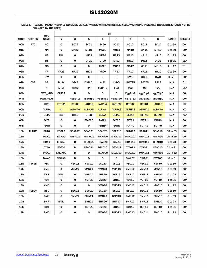
Register DescriptionsThe battery-backed registers are accessible following a slave byte of “1101111x” and reads or writes to addresses [00h:2Fh]. The defined addresses and default values are described in Table 1. The battery backed general purpose SRAM has a different slave address (1010111x), so it is not possible to read/write that section of memory while accessing the registers.
REGISTER ACCESSThe contents of the registers can be modified by performing a byte or a page write operation directly to any register address.
The registers are divided into 8 sections. They are:
1. Real Time Clock (7 bytes): Address 00h to 06h.
2. Control and Status (9 bytes): Address 07h to 0Fh.
3. Alarm (6 bytes): Address 10h to 15h.
4. Time Stamp for Battery Status (5 bytes): Address 16h to 1Ah.
5. Time Stamp for VDD Status (5 bytes): Address 1Bh to 1Fh.
6. Daylight Savings Time (8 bytes): 20h to 27h.
7. TEMP (2 bytes): 28h to 29h
8. Crystal Net PPM Correction, NPPM (2 bytes): 2Ah, 2Bh
10. Crystal ALPHA at high temperature, ALPHA_H (1 byte): 2Dh
11. Scratch Pad (2 bytes): Address 2Eh and 2Fh
Write capability is allowable into the RTC registers (00h to 06h) only when the WRTC bit (bit 6 of address 08h) is set to “1”. A multi-byte read or write operation should be limited to one section per operation for best RTC timekeeping performance.
A register can be read by performing a random read at any address at any time. This returns the contents of that register location. Additional registers are read by performing a sequential read. For the RTC and Alarm registers, the read instruction latches all clock registers into a buffer, so an update of the clock does not change the time being read. At the end of a read, the master supplies a stop condition to end the operation and free the bus. After a read, the address remains at the previous address +1 so the user can execute a current address read and continue reading the next register. When the previous address is 2Fh, the next address will wrap around to 00h.
It is not necessary to set the WRTC bit prior to writing into the control and status, alarm and user SRAM registers.
RTC REGISTERS (SC, MN, HR, DT, MO, YR, DW)These registers depict BCD representations of the time. As such, SC (Seconds) and MN (Minutes) range from 0 to 59, HR (Hour) can either be a 12-hour or 24-hour mode, DT (Date) is 1 to 31, MO (Month) is 1 to 12, YR (Year) is 0 to 99 and DW (Day of the Week) is 0 to 6.
The DW register provides a Day of the Week status and uses three bits DW2 to DW0 to represent the seven days of the week. The counter advances in the cycle 0-1-2-3-4-5-6-0-1-2-… The assignment of a numerical value to a specific day of the week is arbitrary and may be decided by the system software designer. The default value is defined as “0”.
24-HOUR TIMEIf the MIL bit of the HR register is “1”, the RTC uses a 24-hour format. If the MIL bit is “0”, the RTC uses a 12-hour format and HR21 bit functions as an AM/PM indicator with a “1” representing PM. The clock defaults to 12-hour format time with HR21 = “0”.
LEAP YEARSLeap years add the day February 29 and are defined as those years that are divisible by 4. Years divisible by 100 are not leap years, unless they are also divisible by 400. This means that the year 2000 is a leap year and the year 2100 is not. The ISL12020M does not correct for the leap year in the year 2100.
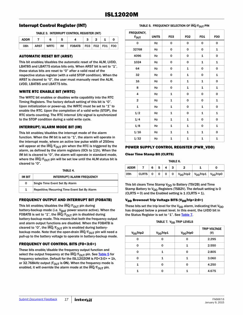
Control and Status Registers (CSR)Addresses [07h to 0Fh]The Control and Status Registers consist of the Status Register, Interrupt and Alarm Register, Analog Trimming and Digital Trimming Registers.
Status Register (SR) The Status Register is located in the memory map at address 07h. This is a volatile register that provides either control or status of RTC failure (RTCF), Battery Level Monitor (LBAT85, LBAT75), alarm trigger, Daylight Saving Time, crystal oscillator enable and temperature conversion in progress bit.
TABLE 1. REGISTER MEMORY MAP (X INDICATES DEFAULT VARIES WITH EACH DEVICE. YELLOW SHADING INDICATES THOSE BITS SHOULD NOT BE CHANGED BY THE USER) (Continued)
BUSY BIT (BUSY)Busy Bit indicates temperature sensing is in progress. In this mode, Alpha, Beta and ITRO registers are disabled and cannot be accessed.
OSCILLATOR FAIL BIT (OSCF)Oscillator Fail Bit indicates that the oscillator has failed. The oscillator frequency is either zero or very far from the desired 32.768kHz due to failure, PC board contamination or mechanical issues.
DAYLIGHT SAVING TIME CHANGE BIT (DSTADJ)DSTADJ is the Daylight Saving Time Adjusted Bit. It indicates the daylight saving time forward adjustment has happened. If a DST Forward event happens, DSTADJ will be set to “1”. The DSTADJ bit will stay high when DSTFD event happens and will be reset to “0” when the DST Reverse event happens. It is read-only and cannot be written. Setting time during a DST forward period will not set this bit to “1”.
The DSTE bit must be enabled when the RTC time is more than one hour before the DST Forward or DST Reverse event time setting, or the DST event correction will not happen.
DSTADJ is reset to “0” upon power-up. It will reset to “0” when the DSTE bit in Register 15h is set to “0” (DST disabled), but no time adjustment will happen.
ALARM BIT (ALM)This bit announces if the alarm matches the real time clock. If there is a match, the respective bit is set to “1”. This bit can be manually reset to “0” by the user or automatically reset by enabling the auto-reset bit (see ARST bit). A write to this bit in the SR can only set it to “0”, not “1”. An alarm bit that is set by an alarm occurring during an SR read operation will remain set after the read operation is complete.
LOW VDD INDICATOR BIT (LVDD)This bit indicates when VDD has dropped below the pre-selected trip level (Brownout Mode). The trip points for the brownout levels are selected by three bits: VDDTrip2, VDDTrip1 and VDDTrip0 in PWR_VDD registers. The LVDD detection is only enabled in VDD mode and the detection happens in real time. The LVDD bit is set whenever the VDD has dropped below the preselected trip level and self clears whenever the VDD is above the preselected trip level.
LOW BATTERY INDICATOR 85% BIT (LBAT85)In Normal Mode (VDD), this bit indicates when the battery level has dropped below the preselected trip levels. The trip points are selected by three bits: VB85Tp2, VB85Tp1 and VB85Tp0 in the PWR_VBAT registers. The LBAT85 detection happens automatically once every minute when seconds register reaches 59. The detection can also be manually triggered by setting the TSE bit in BETA register to “1”. The LBAT85 bit is set when the VBAT has dropped below the preselected trip level and will self
clear when the VBAT is above the pre-selected trip level at the next detection cycle either by manual or automatic trigger.
In Battery Mode (VBAT), this bit indicates the device has entered into battery mode by polling once every 10 minutes. The LBAT85 detection happens automatically once when the minute register reaches x9h or x0h minutes.
Example - When the LBAT85 is Set To “1” In Battery Mode:
The minute the register changes to 19h when the device is in battery mode, the LBAT85 is set to “1” the next time the device switches back to Normal Mode.
Example - When the LBAT85 Remains at “0” In Battery Mode:
If the device enters into battery mode after the minute register reaches 20h and switches back to Normal Mode before the minute register reaches 29h, then the LBAT85 bit will remain at “0” the next time the device switches back to Normal Mode.
LOW BATTERY INDICATOR 75% BIT (LBAT75)In Normal Mode (VDD), this bit indicates when the battery level has dropped below the preselected trip levels. The trip points are selected by three bits: VB75Tp2, VB75Tp1 and VB75Tp0 in the PWR_VBAT registers. The LBAT75 detection happens automatically once every minute when seconds register reaches 59. The detection can also be manually triggered by setting the TSE bit in BETA register to “1”. The LBAT75 bit is set when the VBAT has dropped below the preselected trip level and will self clear when the VBAT is above the preselected trip level at the next detection cycle either by manual or automatic trigger.
In Battery Mode (VBAT), this bit indicates the device has entered into battery mode by polling once every 10 minutes. The LBAT85 detection happens automatically once when the minute register reaches x9h or x0h minutes.
Example - When the LBAT75 is Set to “1” in Battery Mode:
The minute register changes to 30h when the device is in battery mode, the LBAT75 is set to “1” the next time the device switches back to Normal Mode.
Example - When the LBAT75 Remains at “0” in Battery Mode:
If the device enters into battery mode after the minute register reaches 49h and switches back to Normal Mode before minute register reaches 50h, then the LBAT75 bit will remain at “0” the next time the device switches back to Normal Mode.
REAL TIME CLOCK FAIL BIT (RTCF)This bit is set to a “1” after a total power failure. This is a read only bit that is set by hardware (ISL12020M internally) when the device powers up after having lost all power (defined as VDD = 0V and VBAT = 0V). The bit is set regardless of whether VDD or VBAT is applied first. The loss of only one of the supplies does not set the RTCF bit to “1”. The first valid write to the RTC section after a complete power failure resets the RTCF bit to “0” (writing one byte is sufficient).
AUTOMATIC RESET BIT (ARST)This bit enables/disables the automatic reset of the ALM, LVDD, LBAT85 and LBAT75 status bits only. When ARST bit is set to “1”, these status bits are reset to “0” after a valid read of the respective status register (with a valid STOP condition). When the ARST is cleared to “0”, the user must manually reset the ALM, LVDD, LBAT85 and LBAT75 bits.
WRITE RTC ENABLE BIT (WRTC)The WRTC bit enables or disables write capability into the RTC Timing Registers. The factory default setting of this bit is “0”. Upon initialization or power-up, the WRTC must be set to “1” to enable the RTC. Upon the completion of a valid write (STOP), the RTC starts counting. The RTC internal 1Hz signal is synchronized to the STOP condition during a valid write cycle.
INTERRUPT/ALARM MODE BIT (IM)This bit enables/disables the interrupt mode of the alarm function. When the IM bit is set to “1”, the alarm will operate in the interrupt mode, where an active low pulse width of 250ms will appear at the IRQ/FOUT pin when the RTC is triggered by the alarm, as defined by the alarm registers (0Ch to 11h). When the IM bit is cleared to “0”, the alarm will operate in standard mode, where the IRQ/FOUT pin will be set low until the ALM status bit is cleared to “0”.
FREQUENCY OUTPUT AND INTERRUPT BIT (FOBATB)This bit enables/disables the IRQ/FOUT pin during battery-backup mode (i.e. VBAT power source active). When the FOBATB is set to “1”, the IRQ/FOUT pin is disabled during battery-backup mode. This means that both the frequency output and alarm output functions are disabled. When the FOBATB is cleared to “0”, the IRQ/FOUT pin is enabled during battery-backup mode. Note that the open-drain IRQ/FOUT pin will need a pull-up to the battery voltage to operate in battery-backup mode.
FREQUENCY OUT CONTROL BITS (FO<3:0>)These bits enable/disable the frequency output function and select the output frequency at the IRQ/FOUT pin. See Table 5 for frequency selection. Default for the ISL12020M is FO<3:0> = 1h, or 32.768kHz output (FOUT is ON). When the frequency mode is enabled, it will override the alarm mode at the IRQ/FOUT pin.
POWER SUPPLY CONTROL REGISTER (PWR_VDD)
Clear Time Stamp Bit (CLRTS)
This bit clears Time Stamp VDD to Battery (TSV2B) and Time Stamp Battery to VDD Registers (TSB2V). The default setting is 0 (CLRTS = 0) and the Enabled setting is 1 (CLRTS = 1).
VDD Brownout Trip Voltage BITS (VDDTrip<2:0>)
These bits set the trip level for the VDD alarm, indicating that VDD has dropped below a preset level. In this event, the LVDD bit in the Status Register is set to “1”. See Table 7.
BATTERY VOLTAGE TRIP VOLTAGE REGISTER (PWR_VBAT)This register controls the trip points for the two VBAT alarms, with levels set to approximately 85% and 75% of the nominal battery level.
RESEAL BIT (RESEALB)This is the Reseal bit for actively disconnecting VBAT pin from the internal circuitry. Setting this bit allows the device to disconnect the battery and eliminate standby current drain while the device is unused. Once VDD is powered up, this bit is reset and the VBAT pin is then connected to the internal circuitry.
The application for this bit involves placing the chip on a board with a battery and testing the board. Once the board is tested and ready to ship, it is desirable to disconnect the battery to keep it fresh until the board or unit is placed into final use. Setting RESEALB = “1” initiates the battery disconnect and after VDD power is cycled down and up again, the RESEAL bit is cleared to “0”.
BATTERY LEVEL MONITOR TRIP BITS (VB85TP<2:0>)Three bits select the first alarm (85% of Nominal VBAT) level for the battery voltage monitor. There are total of 7 levels that could be selected for the first alarm. Any of the of levels could be selected as the first alarm with no reference as to nominal battery voltage level. See Table 9.
BATTERY LEVEL MONITOR TRIP BITS (VB75TP<2:0>)Three bits select the second alarm (75% of Nominal VBAT) level for the battery voltage monitor. There are total of 7 levels that could be selected for the second alarm. Any of the of levels could be selected as the second alarm with no reference as to nominal Battery voltage level. See Table 10.
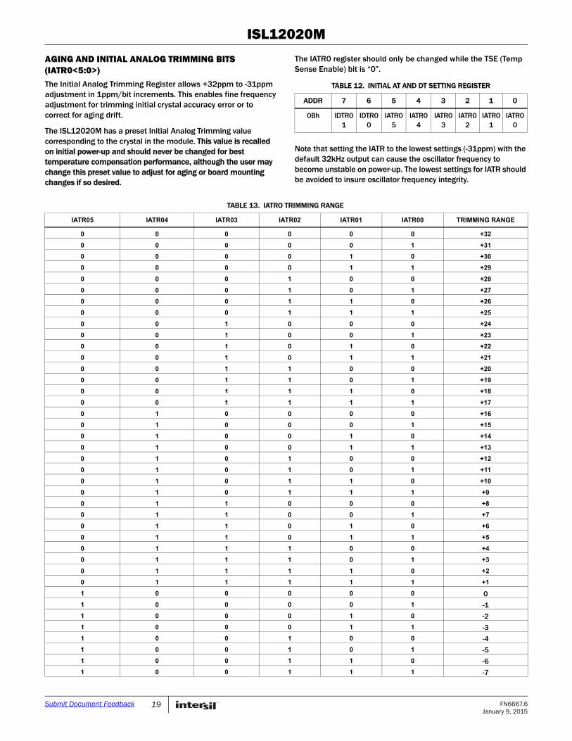
Initial AT and DT setting Register (ITRO)These bits are used to trim the initial error (at room temperature) of the crystal. Both Digital Trimming (DT) and Analog Trimming (AT) methods are available. The digital trimming uses clock pulse skipping and insertion for frequency adjustment. Analog trimming uses load capacitance adjustment to pull the oscillator frequency. A range of +62.5ppm to -61.5ppm is possible with combined digital and analog trimming.
Initial values for the ITR0 register are preset internally and recalled to RAM registers on power-up. These values can be overwritten by the user although this is not suggested as the resulting temperature compensation performance will be compromised. Aging adjustment is normally a few ppm and can be handled by writing to the IATR section.
AGING AND INITIAL TRIM DIGITAL TRIMMING BITS (IDTR0<1:0>)These bits allow ±30.5ppm initial trimming range for the crystal frequency. This is meant to be a coarse adjustment if the range needed is outside that of the IATR control. See Table 11. The IDTR0 register should only be changed while the TSE (Temp Sense Enable) bit is “0”.
The ISL12020M has a preset Initial Digital Trimming value corresponding to the crystal in the module. This value is recalled on initial power-up and should never be changed for best temperature compensation performance, although the user may change this preset value to adjust for aging or board mounting changes if so desired.
AGING AND INITIAL ANALOG TRIMMING BITS (IATR0<5:0>)The Initial Analog Trimming Register allows +32ppm to -31ppm adjustment in 1ppm/bit increments. This enables fine frequency adjustment for trimming initial crystal accuracy error or to correct for aging drift.
The ISL12020M has a preset Initial Analog Trimming value corresponding to the crystal in the module. This value is recalled on initial power-up and should never be changed for best temperature compensation performance, although the user may change this preset value to adjust for aging or board mounting changes if so desired.
The IATR0 register should only be changed while the TSE (Temp Sense Enable) bit is “0”.
Note that setting the IATR to the lowest settings (-31ppm) with the default 32kHz output can cause the oscillator frequency to become unstable on power-up. The lowest settings for IATR should be avoided to insure oscillator frequency integrity.
TABLE 12. INITIAL AT AND DT SETTING REGISTER
ADDR 7 6 5 4 3 2 1 0
0Bh IDTR01
IDTR00
IATR05
IATR04
IATR03
IATR02
IATR01
IATR00
TABLE 13. IATRO TRIMMING RANGE
IATR05 IATR04 IATR03 IATR02 IATR01 IATR00 TRIMMING RANGE
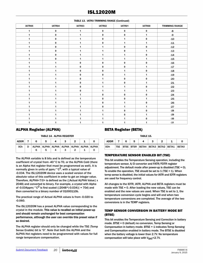
The ALPHA variable is 8 bits and is defined as the temperature coefficient of crystal from -40°C to T0, or the ALPHA Cold (there is an Alpha Hot register that must be programmed as well). It is normally given in units of ppm/°C2, with a typical value of -0.034. The ISL12020M device uses a scaled version of the absolute value of this coefficient in order to get an integer value. Therefore, ALPHA<7:0> is defined as the (|Actual ALPHA Value| x 2048) and converted to binary. For example, a crystal with Alpha of -0.034ppm/°C2 is first scaled (|2048*(-0.034)| = 70d) and then converted to a binary number of 01000110b.
The practical range of Actual ALPHA values is from -0.020 to -0.060.
The ISL12020M has a preset ALPHA value corresponding to the crystal in the module. This value is recalled on initial power-up and should remain unchanged for best compensation performance, although the user can override this preset value if so desired.
The ALPHA register should only be changed while the TSE (Temp Sense Enable) bit is “0”. Note that both the ALPHA and the ALPHA Hot registers need to be programmed with values for full range temperature compensation.
BETA Register (BETA)
TEMPERATURE SENSOR ENABLED BIT (TSE)This bit enables the Temperature Sensing operation, including the temperature sensor, A/D converter and FATR/FDTR register adjustment. The default mode after power-up is disabled (TSE = 0). To enable the operation, TSE should be set to 1 (TSE = 1). When temp sense is disabled, the initial values for IATR and IDTR registers are used for frequency control.
All changes to the IDTR, IATR, ALPHA and BETA registers must be made with TSE = 0. After loading the new values, TSE can be enabled and the new values are used. When TSE is set to 1, the temperature conversion cycle begins and will end when two temperature conversions are completed. The average of the two conversions is in the TEMP registers.
TEMP SENSOR CONVERSION IN BATTERY MODE BIT (BTSE)This bit enables the Temperature Sensing and Correction in battery mode. BTSE = 0 (default) no conversion, Temp Sensing or Compensation in battery mode. BTSE = 1 indicates Temp Sensing and Compensation enabled in battery mode. The BTSE is disabled when the battery voltage is lower than 2.7V. No temperature compensation will take place with VBAT<2.7V.
FREQUENCY OF TEMPERATURE SENSING AND CORRECTION BIT (BTSR)This bit controls the frequency of Temp Sensing and Correction. BTSR = 0 default mode is every 10 minutes, BTSR = 1 is every 1.0 minute. Note that BTSE has to be enabled in both cases. See Table 16.
The temperature measurement conversion time is the same for battery mode as for VDD mode, approximately 22ms. The battery mode current will increase during this conversion time to typically 68µA. The average increase in battery current is much lower than this due to the small duty cycle of the ON-time versus OFF-time for the conversion.
To figure the average increase in battery current, we take the change in current times the duty cycle. For the 1 minute temperature period the average current is as shown in Equation 1:
For the 10 minute temperature period the average current is as shown in Equation 2:
If the application has a stable temperature environment that doesn’t change quickly, the 10 minute option will work well and the backup battery lifetime impact is minimized. If quick temperature variations are expected (multiple cycles of more than 10° within an hour), then the 1 minute option should be considered and the slightly higher battery current figured into overall battery life.
GAIN FACTOR OF AT BIT (BETA<4:0>)Beta is specified to take care of the Cm variations of the crystal. Most crystals specify Cm around 2.2fF. For example, if Cm > 2.2fF, the actual AT steps may reduce from 1ppm/step to approximately 0.80ppm/step. Beta is then used to adjust for this variation and restore the step size to 1ppm/step.
BETA values are limited in the range from 01000 to 11111 as shown in Table 17. To use Table 17, the device is tested at two AT settings in Equation 3:
Where:
AT(max) = FOUT in ppm (at AT = 00H) and
AT(min) = FOUT in ppm (at AT = 3FH).
The BETA VALUES result is indexed in the right hand column and the resulting Beta factor (for the register) is in the same row in the left column.
The ISL12020M has a preset BETA value corresponding to the crystal in the module. This value is recalled on initial power-up and should never be changed for best temperature compensation performance, although the user may override this preset value if so desired.
The value for BETA should only be changed while the TSE (Temp Sense Enable) bit is “0”. The procedure for writing the BETA register involves two steps. First, write the new value of BETA with TSE = 0. Then write the same value of BETA with TSE = 1. This will insure the next temp sense cycle will use the new BETA value.
TABLE 16. FREQUENCY OF TEMPERATURE SENSING AND CORRECTION BIT
Final Analog Trimming Register (FATR)This register shows the final setting of AT after temperature correction. It is read-only; the user cannot overwrite a value to this register. This value is accessible as a means of monitoring the temperature compensation function. See Tables 18 and 19 (for values).
Final Digital Trimming Register (FDTR)This register shows the final setting of DT after temperature correction. It is read-only; the user cannot overwrite a value to this register. The value is accessible as a means of monitoring the temperature compensation function. The corresponding clock adjustment values are shown in Table 20. The FDTR setting has both positive and negative settings to adjust for any offset in the crystal..
ALARM Registers (10h to 15h)The alarm register bytes are set up identical to the RTC register bytes, except that the MSB of each byte functions as an enable bit (enable = “1”). These enable bits specify which alarm registers (seconds, minutes, etc.) are used to make the comparison. Note that there is no alarm byte for year.
The alarm function works as a comparison between the alarm registers and the RTC registers. As the RTC advances, the alarm will be triggered once a match occurs between the alarm registers and the RTC registers. Any one alarm register, multiple registers, or all registers can be enabled for a match.
There are two alarm operation modes: Single Event and periodic Interrupt Mode:
• Single Event Mode is enabled by setting the bit 7 on any of the Alarm registers (ESCA0... EDWA0) to “1”, the IM bit to “0” and disabling the frequency output. This mode permits a one-time match between the Alarm registers and the RTC registers. Once this match occurs, the ALM bit is set to “1” and the IRQ/FOUT output will be pulled low and will remain low until the ALM bit is reset. This can be done manually or by using the auto-reset feature.
• Interrupt Mode is enabled by setting the bit 7 on any of the Alarm registers (ESCA0... EDWA0) to “1”, the IM bit to “1” and disabling the frequency output. The IRQ/FOUT output will now be pulsed each time an alarm occurs. This means that once the interrupt mode alarm is set, it will continue to alarm for each occurring match of the alarm and present time. This mode is convenient for hourly or daily hardware interrupts in microcontroller applications such as security cameras or utility meter reading.
To clear a single event alarm, the ALM bit in the status register must be set to “0” with a write. Note that if the ARST bit is set to 1 (address 08h, bit 7), the ALM bit will automatically be cleared when the status register is read.
Following are examples of both Single Event and periodic Interrupt Mode alarms.
Example 1
• Alarm set with single interrupt (IM = “0”)
• A single alarm will occur on January 1 at 11:30 a.m.
• Set Alarm registers as follows:
TABLE 18. FINAL ANALOG TRIMMING REGISTER
ADDR 7 6 5 4 3 2 1 0
0Eh 0 0 FATR5 FATR4 FATR3 FATR2 FATR1 FATR0
TABLE 19. FINAL DIGITAL TRIMMING REGISTER
ADDR 7 6 5 4 3 2 1 0
0Fh 0 0 0 FDTR4 FDTR3 FDTR2 FDTR1 FDTR0
TABLE 20. CLOCK ADJUSTMENT VALUES FOR FINAL DIGITAL TRIMMING REGISTER
After these registers are set, an alarm will be generated when the RTC advances to exactly 11:30 a.m. on January 1 (after seconds changes from 59 to 00) by setting the ALM bit in the status register to “1” and also bringing the IRQ/FOUT output low.
Example 2
• Pulsed interrupt once per minute (IM = “1”)
• Interrupts at one minute intervals when the seconds register is at 30s.
• Set Alarm registers as follows:
Once the registers are set, the following waveform will be seen at IRQ/FOUT:
Note that the status register ALM bit will be set each time the alarm is triggered, but does not need to be read or cleared.
Time Stamp VDD to Battery Registers (TSV2B)The TSV2B Register bytes are identical to the RTC register bytes, except they do not extend beyond the Month. The Time Stamp
captures the FIRST VDD to Battery Voltage transition time and will not update upon subsequent events, until cleared (only the first event is captured before clearing). Set CLRTS = 1 to clear this register (Add 09h, PWR_VDD register).
Note that the time stamp registers are cleared to all “0”, including the month and day, which is different from the RTC and alarm registers (those registers default to 01h). This is the indicator that no time stamping has occurred since the last clear or initial power-up. Once a time stamp occurs, there will be a non-zero time stamp.
Time Stamp Battery to VDD Registers (TSB2V)The Time Stamp Battery to VDD Register bytes are identical to the RTC register bytes, except they do not extend beyond Month. The Time Stamp captures the LAST transition of VBAT to VDD (only the last event of a series of power-up/down events is retained). Set CLRTS = 1 to clear this register (Add 09h, PWR_VDD register).
DST Control Registers (DSTCR)8 bytes of control registers have been assigned for the Daylight Savings Time (DST) functions. DST beginning (set Forward) time is controlled by the registers DstMoFd, DstDwFd, DstDtFd and DstHrFd. DST ending time (set Backward or Reverse) is controlled by DstMoRv, DstDwRv, DstDtRv and DstHrRv.
Tables 23 and 24 describe the structure and functions of the DSTCR.
DST FORWARD REGISTERS (20H TO 23H)DST forward is controlled by the following DST Registers:
DST Enable
DSTE is the DST Enabling Bit located in Bit 7 of register 20h (DstMoFdxx). Set DSTE = 1 will enable the DSTE function. Upon powering up for the first time (including battery), the DSTE bit defaults to “0”. When DSTE is set to “1” the RTC time must be at least one hour before the scheduled DST time change for the correction to take place. When DSTE is set to “0”, the DSTADJ bit in the Status Register automatically resets to “0”.
DST Month Forward
DstMoFd sets the Month that DST starts. The format is the same as for the RTC register month, from 1 to 12. The default value for the DST begin month is 00h.
DST Day/Week Forward
DstDwFd contains both the Day of the Week and the Week of the Month data for DST Forward control. DST can be controlled either by actual date or by setting both the Week of the month and the Day of the Week. DstDwFdE sets the priority of the Day/Week over the Date. For DstDwFdE = 1, Day/Week is the priority. You must have the correct Day of Week entered in the RTC registers for the Day/Week correction to work properly.
TABLE 21.
ALARMREGISTER
BIT
DESCRIPTION7 6 5 4 3 2 1 0 HEX
SCA0 0 0 0 0 0 0 0 0 00h Seconds disabled
MNA0 1 0 1 1 0 0 0 0 B0h Minutes set to 30, enabled
HRA0 1 0 0 1 0 0 0 1 91h Hours set to 11, enabled
DTA0 1 0 0 0 0 0 0 1 81h Date set to 1, enabled
MOA0 1 0 0 0 0 0 0 1 81h Month set to 1, enabled
DWA0 0 0 0 0 0 0 0 0 00h Day of week disabled
TABLE 22.
ALARMREGISTER
BIT
DESCRIPTION7 6 5 4 3 2 1 0 HEX
SCA0 1 0 1 1 0 0 0 0 B0h Seconds set to 30, enabled
• Bits 0, 1, 2 contain the Day of the week information, which sets the Day of the Week that DST starts. Note that Day of the week counts from 0 to 6, like the RTC registers. The default for the DST Forward Day of the Week is 00h (normally Sunday).
• Bits 3, 4, 5 contain the Week of the Month information that sets the week that DST starts. The range is from 1 to 5 and Week 7 is used to indicate the last week of the month. The default for the DST Forward Week of the Month is 00h.
DST Date Forward
DstDtfd controls which Date DST begins. The format for the Date is the same as for the RTC register, from 1 to 31. The default value for DST forward date is 00h. DstDtFd is only effective if DstDwFdE = 0.
DST Hour Forward
DstHrFd controls the hour that DST begins. The RTC hour and DstHrFd registers have the same formats except there is no Military bit for DST hour. The user sets the DST hour with the same format as used for the RTC hour (AM/PM or MIL) but without the MIL bit and the DST will still advance as if the MIL bit were there. The default value for DST hour Forward is 00h.
DST REVERSE REGISTERS (24H TO 27H)DST end (reverse) is controlled by the following DST Registers:
DST Month Reverse
DstMoRv sets the Month that DST ends. The format is the same as for the RTC register month, from 1 to 12. The default value for the DST end month is October (10h).
DST Day/Week Reverse
DstDwRv contains both the Day of the Week and the Week of the Month data for DST Reverse control. DST can be controlled either by actual date or by setting both the Week of the month and the Day of the Week. DstDwRvE sets the priority of the Day/Week over the Date. For DstDwRvE = 1, Day/Week is the priority. You
must have the correct Day of Week entered in the RTC registers for the Day/Week correction to work properly.
• Bits 0, 1, 2 contain the Day of the week information, which sets the Day of the Week that DST ends. Note that Day of the week counts from 0 to 6, like the RTC registers. The default for the DST Reverse Day of the Week is 00h (normally Sunday).
• Bits 3, 4, 5 contain the Week of the Month information that sets the week that DST ends. The range is from 1 to 5 and Week 7 is used to indicate the last week of the month. The default for the DST Reverse Week of the Month is 00h.
DST Date Reverse
DstDtRv controls which Date DST ends. The format for the Date is the same as for the RTC register, from 1 to 31. The default value for DST Date Reverse is 00h. The DstDtRv is only effective if the DwRvE = 0.
DST Hour Reverse
DstHrRv controls the hour that DST ends. The RTC hour and DstHrFd registers have the same formats except there is no Military bit for DST hour. The user sets the DST hour with the same format as used for the RTC hour (AM/PM or MIL) but without the MIL bit and the DST will still advance as if the MIL bit were there. The default value for DST hour Reverse is 00h.
TEMP Registers (TEMP) The temperature sensor produces an analog voltage output, which is input to an A/D converter and produces a 10-bit temperature value in degrees Kelvin. TK07:00 are the LSBs of the code and TK09:08 are the MSBs of the code. The temperature result is actually the average of two successive temperature measurements to produce greater resolution for the temperature control. The output code can be converted to degrees Centigrade by first converting from binary to decimal, dividing by 2 and then subtracting 273d.
The practical range for the temp sensor register output is from 446d to 726d, or -50°C to +90°C. The temperature compensation function is only guaranteed over -40°C to +85°C. The TSE bit must be set to “1” to enable temperature sensing.
NPPM Registers (NPPM) The NPPM value is exactly 2x the net correction required to bring the oscillator to 0ppm error. The value is the combination of oscillator Initial Correction (IPPM) and crystal temperature dependent correction (CPPM).
IPPM is used to compensate the oscillator offset at room temperature and is controlled by the ITR0 and BETA registers, which are fixed during factor test.
The CPPM compensates the oscillator frequency fluctuation over temperature. It is determined by the temperature (T), crystal curvature parameter (ALPHA) and crystal turn-over temperature (XT0). T is the result of the temp sensor/ADC conversion, whose decimal result is 2x the actual temperature in Kelvin. ALPHA is from either the ALPHA (cold) or ALPHAH (hot) register depending on T and XT0 is from the XT0 register.
NPPM is governed by Equation 5:
NPPM = IPPM(ITR0,BETA) + ALPHA x (T-T0)2
Where
T is the reading of the ADC, result is 2 x temperature in degrees Kelvin.
or
Note that NPPM can also be predicted from the FATR and FDTR register by the relationship (all values in decimal):
NPPM = 2*(BETA*FATR - (FDTR-16))
XT0 Registers (XT0)
TURNOVER TEMPERATURE (XT<3:0>)The apex of the Alpha curve occurs at a point called the turnover temperature, or XT0. Crystals normally have a turnover temperature between +20°C and +30°C, with most occurring near +25°C.
The ISL12020M has a preset turnover temperature corresponding to the crystal in the module. This value is recalled on initial power-up and should never be changed for best temperature compensation performance, although the user may override this preset value if so desired.
Table 27 shows the values available, with a range from +17.5°C to +32.5°C in +0.5°C increments. The default value is 00000b or +25°C.
The ALPHA Hot variable is 7 bits and is defined as the temperature coefficient of Crystal from the XT0 value to +85°C (both Alpha Hot and Alpha Cold must be programmed to provide full temperature compensation). It is normally given in units of ppm/°C2, with a typical value of -0.034. Like the ALPHA cold version, a scaled version of the absolute value of this coefficient is used in order to get an integer value. Therefore, ALP_H<7:0> is defined as the (|Actual Alpha Hot Value| x 2048) and converted to binary. For example, a crystal with Alpha Hot of -0.034ppm/°C2 is first scaled (|2048*(-0.034)| = 70d) and then converted to a binary number of 01000110b.
The practical range of Actual ALPHAH values is from -0.020 to -0.060.
The ISL12020M has a preset ALPHAH value corresponding to the crystal in the module. This value is recalled on initial power-up and should never be changed for best temperature compensation performance, although the user may override this preset value if so desired.
The ALPHAH register should only be changed while the TSE (Temp Sense Enable) bit is “0”.
User Registers (Accessed by Using Slave Address 1010111x)Addresses [00h to 7Fh]These registers are 128 bytes of battery-backed user SRAM. The separate I2C slave address must be used to read and write to these registers.
I2C Serial Interface The ISL12020M supports a bidirectional bus oriented protocol. The protocol defines any device that sends data onto the bus as a transmitter and the receiving device as the receiver. The device controlling the transfer is the master and the device being controlled is the slave. The master always initiates data transfers and provides the clock for both transmit and receive operations. Therefore, the ISL12020M operates as a slave device in all applications.
All communication over the I2C interface is conducted by sending the MSB of each byte of data first.
Protocol ConventionsData states on the SDA line can change only during SCL LOW periods. SDA state changes during SCL HIGH are reserved for indicating START and STOP conditions (see Figure 16). On power-up of the ISL12020M, the SDA pin is in the input mode..
11110 18.0
11111 17.5
TABLE 28. ALPHA HOT REGISTER
ADDR 7 6 5 4 3 2 1 0
2Dh D ALP_H6
ALP_H5
ALP_H4
ALP_H3
ALP_H2
ALP_H1
ALP_H0
TABLE 27. XT0 VALUES (Continued)
XT<4:0> TURNOVER TEMPERATURE
FIGURE 16. VALID DATA CHANGES, START AND STOP CONDITIONS
All I2C interface operations must begin with a START condition, which is a HIGH-to-LOW transition of SDA while SCL is HIGH. The ISL12020M continuously monitors the SDA and SCL lines for the START condition and does not respond to any command until this condition is met (see Figure 16). A START condition is ignored during the power-up sequence.
All I2C interface operations must be terminated by a STOP condition, which is a LOW-to-HIGH transition of SDA while SCL is HIGH (see Figure 16). A STOP condition at the end of a read operation or at the end of a write operation to memory only places the device in its standby mode.
An acknowledge (ACK) is a software convention used to indicate a successful data transfer. The transmitting device, either master or slave, releases the SDA bus after transmitting eight bits. During the ninth clock cycle, the receiver pulls the SDA line LOW to acknowledge the reception of the eight bits of data (see Figure 17).
The ISL12020M responds with an ACK after recognition of a START condition followed by a valid Identification Byte and once again, after successful receipt of an Address Byte. The ISL12020M also responds with an ACK after receiving a Data Byte of a write operation. The master must respond with an ACK after receiving a Data Byte of a read operation.
Device AddressingFollowing a start condition, the master must output a Slave Address Byte. The 7 MSBs are the device identifiers. These bits are “1101111” for the RTC registers and “1010111” for the User SRAM.
The last bit of the Slave Address Byte defines a read or write operation to be performed. When this R/W bit is a “1”, a read operation is selected. A “0” selects a write operation (refer to Figure 19).
After loading the entire Slave Address Byte from the SDA bus, the ISL12020M compares the device identifier and device select bits with “1101111” or “1010111”. Upon a correct compare, the device outputs an acknowledge on the SDA line.
Following the Slave Byte is a one byte word address. The word address is either supplied by the master device or obtained from an internal counter. On power-up, the internal address counter is set to address 00h, so a current address read starts at address 00h. When required, as part of a random read, the master must supply the 1 Word Address Bytes, as shown in Figure 20.
In a random read operation, the slave byte in the “dummy write” portion must match the slave byte in the “read” section. For a random read of the Control/Status Registers, the slave byte must be “1101111x” in both places.
Write OperationA Write operation requires a START condition, followed by a valid Identification Byte, a valid Address Byte, a Data Byte and a STOP condition. After each of the three bytes, the ISL12020M responds with an ACK. At this time, the I2C interface enters a standby state.
Read OperationA Read operation consists of a three byte instruction, followed by one or more Data Bytes (see Figure 20). The master initiates the operation issuing the following sequence: a START, the Identification byte with the R/W bit set to “0”, an Address Byte, a second START and a second Identification byte with the R/W bit set to “1”. After each of the three bytes, the ISL12020M responds with an ACK. Then the ISL12020M transmits Data Bytes as long as the master responds with an ACK during the SCL cycle following the eighth bit of each byte. The master terminates the read operation (issuing a STOP condition) following the last bit of the last Data Byte (see Figure 20).
The Data Bytes are from the memory location indicated by an internal pointer. This pointer’s initial value is determined by the Address Byte in the Read operation instruction and increments by one during transmission of each Data Byte. After reaching the memory location 2Fh, the pointer “rolls over” to 00h and the device continues to output data for each ACK received.
FIGURE 18. BYTE WRITE SEQUENCE (SLAVE ADDRESS FOR CSR SHOWN)
START
STOP
IDENTIFICATIONBYTE
DATABYTE
ACK
SIGNALS FROMTHE MASTER
SIGNALS FROMTHE ISL12020M
ACK
1 001 1
ACK
WRITE
SIGNAL AT SDA 0 0 0 01 1 1
ADDRESSBYTE
FIGURE 19. SLAVE ADDRESS, WORD ADDRESS AND DATA BYTES
Application SectionPower Supply ConsiderationsThe ISL12022M contains programmed EEPROM registers which are recalled to volatile RAM registers during initial power-up. These registers contain DC voltage, frequency and temperature calibration settings. Initial power-up can be either application of VBAT or VDD power, whichever is first. It is important that the initial power-up meet the power supply slew rate specification to avoid faulty EEPROM power-up recall. Also, any glitches or low voltage DC pauses should be avoided, as these may activate recall at a low voltage and load erroneous data into the calibration registers. Note that a very slow VDD ramp rate (outside data sheet limits) will almost always trigger erroneous recall and should be avoided entirely.
Battery-Backup DetailsThe ISL12020M has automatic switchover to battery-backup when the VDD drops below the VBAT mode threshold. A wide variety of backup sources can be used, including standard and rechargeable lithium, Super Capacitors, or regulated secondary sources. The serial interface is disabled in battery-backup, while the oscillator and RTC registers are operational. The SRAM register contents are powered to preserve their contents as well.
The input voltage range for VBAT is 1.8V to 5.5V, but keep in mind the temperature compensation only operates for VBAT > 2.7V. Note that the device is not guaranteed to operate with a VBAT < 1.8V, so the battery should be changed before discharging to that level. It is strongly advised to monitor the low battery indicators in the status registers and take action to replace discharged batteries.
If a Super Capacitor is used, it is possible that it may discharge to below 1.8V during prolonged power-down. Once powered up, the device may lose serial bus communications until both VDD and VBAT are powered down together. To avoid that situation, including situations where a battery may discharge deeply, the circuit in Figure 21 can be used.
The diode, DBAT, will add a small drop to the battery voltage but will protect the circuit should battery voltage drop below 1.8V. The jumper is added as a safeguard should the battery ever need to be disconnect from the circuit.
.
The VDD negative slew rate should be limited to below the data sheet spec (10V/ms) otherwise battery switchover can be delayed, resulting in SRAM contents corruption and oscillator operation interruption.
Some applications will require separate supplies for the RTC VDD and the I2C pullups. This is not advised, as it may compromise the operation of the I2C bus. For applications that do require serial bus communication with the RTC VDD powered down, the SDA pin must be pulled low during the time the RTC VDD ramps down to 0V. Otherwise, the device may lose serial bus communications once VDD is powered up and will return to normal operation ONLY once VDD and VBAT are both powered down together.
Layout ConsiderationsThe ISL12020M contains a quarts crystal and requires special handling during PC board assembly. Excessive shock and vibrations should be avoided. Ultrasound cleaning is not advisable. See Note 7 on page 6 in the electrical specifications table pertaining to solder reflow effects on oscillator accuracy.
The crystal pins X1 and X2 have a very high impedance and oscillator circuits operating at low frequencies (such as 32.768kHz) are known to pick up noise very easily if layout precautions are not followed. Most instances of erratic clocking or large accuracy errors can be traced to the susceptibility of the oscillator circuit to interference from adjacent high speed clock or data lines. Careful layout of the RTC circuit will avoid noise pickup and insure accurate clocking.
Figure 22 shows a suggested layout for the ISL12020M device. Three main precautions should be followed:
1. Do not run the serial bus lines or any high speed logic lines in the vicinity of the X1 and X2 pins. These logic level lines can induce noise in the oscillator circuit, causing misclocking.
2. Add a ground trace around the device with one end terminated at the chip ground. This guard ring will provide termination for emitted noise in the vicinity of the RTC device.
3. Do not run a ground or power plane immediately under the RTC. This will add capacitance to the X1/X2 pins and change the trimmed frequency of the oscillator. Instead, try to leave a gap in any planes under the RTC device.
.
The best way to run clock lines around the RTC is to stay outside of the ground ring by at least a few millimeters. Also, use the VBAT and VDD as guard ring lines as well, they can isolate clock lines from the X1 and X2 pins. In addition, if the IRQ/FOUT pin is used as a clock, it should be routed away from the RTC device as well.
Measuring Oscillator AccuracyThe best way to analyze the ISL12020M frequency accuracy is to set the IRQ/FOUT pin for a specific frequency and look at the output of that pin on a high accuracy frequency counter (at least 7 digits accuracy). Note that the IRQ/FOUT is an drain output and will require a pull-up resistor.
Using the 1.0Hz output frequency is the most convenient as the ppm error is just as shown in Equation 7:
Other frequencies may be used for measurement but the error calculation becomes more complex.
When the proper layout guidelines above are observed, the oscillator should start-up in most circuits in less than one second. When testing RTC circuits, a common impulse is to apply a scope probe to the circuit at the X2 pin (oscillator output) and observe the waveform. DO NOT DO THIS! Although in some cases you may see a usable waveform, due to the parasitics (usually 10pF to ground) applied with the scope probe, there will be no useful information in that waveform other than the fact that the circuit is oscillating. The X2 output is sensitive to capacitive impedance so the voltage levels and the frequency will be affected by the
parasitic elements in the scope probe. Use the FOUT output and a frequency counter for the most accurate results.
Temperature Compensation OperationThe ISL12020M temperature compensation feature needs to be enabled by the user. This must be done in a specific order as follows:
1. Read register 0Dh, the BETA register. This register contains the 5-bit BETA trimmed value, which is automatically loaded on initial power-up. Mask off the 5LSB’s of the value just read.
2. Bit 7 of the BETA register is the master enable control for temperature sense operation. Set this to “1” to allow continuous temperature frequency correction. Frequency correction will then happen every 60s with VDD applied.
3. Bits 5 and 6 of the BETA register control temperature compensation in battery-backup mode (see Table 16 on page 21). Set the values for the operation desired.
4. Write back to register 0Dh making sure not to change the 5 LSB values and include the desired compensation control bits.
Note that every time the BETA register is written with the TSE bit = 1, a temperature compensation cycle is instigated and a new correction value will be loaded into the FATR/FDTR registers (if the temperature changed since the last conversion).
Also note that registers 0Bh and 0Ch, the ITR0 and ALPHA registers, should not be changed. If they must be written be sure to write the same values that are recalled from initial power-up. The ITR0 register may be written if the user wishes to recalibrate the oscillator frequency at room temperature for aging or board mounting. The original recalled value can be rewritten if desired after testing.
Daylight Savings Time (DST) ExampleDST involves setting the forward and back times and allowing the RTC device to automatically advance the time or set the time back. This can be done for current year and future years. Many regions have DST rules that use standard months, weeks and time of the day, which permit a preprogrammed, permanent setting.
An example setup for the ISL12020M is in Table 29.
FIGURE 22. SUGGESTED LAYOUT FOR ISL12020M
FOUT
SCL
SDA
GROUNDRING
ppm error FOUT 1– 1e6= (EQ. 7)
TABLE 29. DST EXAMPLE
VARIABLE VALUE REGISTER VALUE
Month Forward and DST Enable
April 15h 84h
Week and Day Forward and select Day/Week, not Date
1st Week and Sunday
16h 48h
Date Forward not used 17h 00h
Hour Forward 2am 18h 02h
Month Reverse October 19h 10h
Week and Day Reverse and select Day/Week, not Date
The Enable bit (DSTE) is in the Month forward register, so the BCD value for that register is altered with the additional bit. The Week and Day values along with Week/Day vs Date select bit is in the Week/Day register, so that value is also not straight BCD. Hour and Month are normal BCD, but the Hour doesn’t use the MIL bit since Military time PM values are already discretely different from AM/PM time PM values. The DST reverse setting utilizes the option to select the last week of the month for October, which could have 4 or 5 weeks but needs to have the time change on the last Sunday.
Note that the DSTADJ bit in the status register monitors whether the DST forward adjustment has happened. When it is “1”, DST forward has taken place. When it is “0”, then either DST reverse has happened, or it has been reset either by initial power-up or if the DSTE bit has been set to “0”.
Revision HistoryThe revision history provided is for informational purposes only and is believed to be accurate, but not warranted. Please go to web to make sure you have the latest Rev.
DATE REVISION CHANGE
January 9, 2015 FN6667.6 Updated datasheet applying Intersil’s new standards.On page 1, added bullet (AN1389) to the Related Literature section. Updated the temperature range from “-40°C to +85°C” to “0°C to +85°C” on page 1 in paragraph 1, on page 5 in the Pin Descriptions table for X2 and X1 pins and on page 11 in paragraph 1.On page 7, updated FoutT by the following:
added “0°C to +85°C” to the test conditionsadded “-30°C to +85C” and “-40°C to +85°C” rows
Updated Products verbiage to About Intersil verbiage.
October 28, 2011 FN6667.5 On page 1, corrected Figure 1, Typical Application Circuit to show that pin 6/15 are not connected to ground.On page 4, Ordering Information, added ISL12020MIRZ-EVALZ evaluation board.On page 5, Pin Descriptions, added Ground pin row, separated VDD pin. Bolded No Connection for the Thermal Pad.On page 6, Absolute Maximum Ratings, added shock, vibration.On page 6, for IDD1 at 3V/5V limits, changed MAX from 7/6µA to 15/14µA.On page 7, added VDDSR+ as typical, with Note 17.On page 8, added Note 17 for VDDSR+On page 16, under Oscillator Fail Bit, changed text to: “Oscillator Fail Bit indicates that the oscillator has failed. The oscillator frequency is either zero or very far from the desired 32.768kHz due to failure, PC board contamination or mechanical issues.”On page 16, under Daylight Savings Time Change Bit, removed “DSTADJ can be set to “1” for instances where the RTC device is initialized during the DST Forward period.” Added “It is read-only and cannot be written. Setting time during a DST forward period will not set this bit to “1”.”On page 22, Table 19, changed FDTR column head from <2:0> to <4:0>.On page 22, Tables 20 and 21, corrected addresses.On page 28, added Power Supply Considerations section.
April 23, 2010 Added “Latch-up (Tested per JESD-78B; Class 2, Level A) 100mA or 1.5 * VMAX Input” on page 6Added “Maximum Junction Temperature +85°C” on page 6Added “” on page 1Added “Thermal Pad” description to “Pin Descriptions” on page 5. Added “Thermal Pad” label to “Pin Configuration” on page 5.Added cross references to page numbers in “Revision History”.Updated Package Outline Drawing on page 34 to most recent revision. Changes were as follows:Revised note 8 from:"Soldering required to PCB for X1 and X2 pads each on a separate floating metal (GRN)."to:"Soldering required to PCB for X1 and X2 pads to separate and non-connected metal pads."Changed Note 2 from:"These Intersil plastic packaged products employ special material sets, molding compounds and 100% matte tin plate plus anneal (e3) termination finish. These products do contain Pb but they are RoHS compliant by exemption 7 (lead in high melt temp solder for internal connections) and exemption 5 (lead in piezoelectric elements).." to:"These Intersil plastic packaged products employ special material sets, molding compounds and 100% matte tin plate plus anneal (e3) termination finish. These products do contain Pb but they are RoHS compliant by exemption 7 (lead in high melting temp solder and in piezoelectronic devices) and exemption 5 (lead in glass of electronic components).."
February 11, 2010 FN6667.4 Updated Note 2 in Ordering Information table from “These Intersil Pb-free plastic packaged products employ special Pb-free material sets, molding compounds/die attach materials and 100% matte tin plate plus anneal (e3 termination finish, which is RoHS compliant and compatible with both SnPb and Pb-free soldering operations). Intersil Pb-free products are MSL classified at Pb-free peak reflow temperatures that meet or exceed the Pb-free requirements of IPC/JEDEC J STD-020.” to “These Intersil plastic packaged products employ special material sets, molding compounds and 100% matte tin plate plus anneal (e3) termination finish. These products do contain Pb but they are RoHS compliant by exemption 7 (lead in high melt temp solder for internal connections) and exemption 5 (lead in piezoelectric elements). These Intersil RoHS compliant products are compatible with both SnPb and Pb-free soldering operations. These Intersil RoHS compliant products are MSL classified at Pb-free peak reflow temperatures that meet or exceed the Pb-free requirements of IPC/JEDEC J STD-020.”
Changed "Pb-Free" in page 1 “Features” and page 4 “Ordering Information” to "RoHS Compliant"
October 22, 2009 Converted to New Intersil Template - Matched front page to match ISL12022M with the exception of pinout change from SOIC to DFN. Updated ordering information by numbering all notes, setting up links, added MSL (Moisture Sensitivity Level) note. Updated word "Pinout" to "Pin Configuration". Pin Descriptions updated by adding descriptive text taken from page 9. Deleted Text Pin Descriptions that were on page 9. Changed Thermal information from "Tja 85, Tjc 3" To "Tja 40, Tjc 3.5" to match ASYD in Intrepid. Pb-free reflow link now shown in blue. Updated Notes in Electrical Spec Tables to follow flow of numbers when referenced. Added "boldface limits..." text in Electrical Spec Conditions to indicate Min and Max over-temp. Bolded all over-temp Min and Max values. Added Revision History and Products information with links. Updated POD from Rev0 to Rev1 to match Intrepid. Added Table of Contents.
July 24, 2009 FN6667.3 Page 1: in the Features section, corrected typo in the second bullet from:20 Ld DFN Package (for SOIC package see ISL12020M)To:20 Ld DFN Package (for SOIC package see ISL12022M)No rev, no date change, no formal review necessary
June 22, 2009 Changes in Word document attached in Intrepid. http://intranet.intrepid.intersil.com/Windchill/servlet/WindchillAuthGW/wt.content.ContentHttp/viewContent/12020M.doc?u8&HttpOperationItem=wt.content.ApplicationData%3A120896672&ContentHolder=ext.isil.part.mcol.MCOL%3A120896665
January 15, 2009 FN6667.2 Added text and equations for Ibat for temp sense ON and for relative accuracy for 1m vs 10m intervalAdded text clarifying that no compensation at Vbat<2.7VRevised entire “DAYLIGHT SAVING TIME CHANGE BIT (DSTADJ)” on page 16Added Application Example for DST - “Daylight Savings Time (DST) Example” on page 29Added requirement for Vbat>1.8V in Vbat note.Added apps circuit to survive Vbat<1.8VCorrected all occurrences of Alpha tablesBolded and shaded the COMPENSATION registers in Table 1 to indicate they are not to be overwritten. Also bolded an advisory in the register sections.Fixed blank bits in register tables and in text.Register Table 1: Change default values for compensation to xx's, they are different with each device. Added Datasheet curvesAdded statement to Apps section on crystal handling (in “Layout Considerations” on page 28.)Applied Intersil standards as follows: Updated lead finish note in “Ordering Information”, added Theta JC note for thermal resistance, updated over-temp note in Electrical Specification tables, numbered equations that were not initially, updated POD to latest version, which includes following edits:Note 6 revised from “Soldering required to PCB for X1 and X2 pads each on a separate floating metal (GRN).”to “The X1 and X2 pads need to be soldered down to the PCB on separate and electrically isolated land pads.” Minor dimensions included based on customer input and laid out in new format.On page 6: IDD1 - Changed Max from 6.5 to 7 for VDD = 5V and 5.5 to 6 for VDD = 3V.On page 3: Remove DeltaATLSB specOn page 7: Hysteresis spec - Remove Min and set Typ to 0.05 x VDDon page 8: tHD:DAT - Change Min from 0 to 20On page 14: For Table 1, yellow shaded and bolded XTO and ALPHAH registersOn page 21: Eq. 3 - Changed "BETAVALUES" to "BETA VALUES"On page 29: Eq. 7 - Change "ppmerror" to "ppm error"On page 26: Changed title for Table 28 from “ALPHA REGISTER” to "ALPHA HOT REGISTER"On Page 16: Under “Initial AT and DT setting Register (ITRO)” on page 18, changed range value from 62.6ppm to 62.5ppm.
Revision HistoryThe revision history provided is for informational purposes only and is believed to be accurate, but not warranted. Please go to web to make sure you have the latest Rev. (Continued)
Intersil products are manufactured, assembled and tested utilizing ISO9001 quality systems as notedin the quality certifications found at www.intersil.com/en/support/qualandreliability.html
Intersil products are sold by description only. Intersil Corporation reserves the right to make changes in circuit design, software and/or specifications at any time without notice. Accordingly, the reader is cautioned to verify that data sheets are current before placing orders. Information furnished by Intersil is believed to be accurate and reliable. However, no responsibility is assumed by Intersil or its subsidiaries for its use; nor for any infringements of patents or other rights of third parties which may result from its use. No license is granted by implication or otherwise under any patent or patent rights of Intersil or its subsidiaries.
For information regarding Intersil Corporation and its products, see www.intersil.com
For additional products, see www.intersil.com/en/products.html
About IntersilIntersil Corporation is a leading provider of innovative power management and precision analog solutions. The company's products address some of the largest markets within the industrial and infrastructure, mobile computing and high-end consumer markets.
For the most updated datasheet, application notes, related documentation and related parts, please see the respective product information page found at www.intersil.com.
You may report errors or suggestions for improving this datasheet by visiting www.intersil.com/ask.
Reliability reports are also available from our website at www.intersil.com/support
March 28, 2008 FN6667.1 Removed Min and Max limits for “Oscillator Initial Accuracy” on page 6. Added Typ of ±2, Replaced Note 11 (Parts are 100% tested at +25°C. Temperature limits established by characterization and are not production tested.) with Note 9 (Limits should be considered typical and are not production tested).
February 27, 2008 FN6667.0 Initial Release to web
Revision HistoryThe revision history provided is for informational purposes only and is believed to be accurate, but not warranted. Please go to web to make sure you have the latest Rev. (Continued)