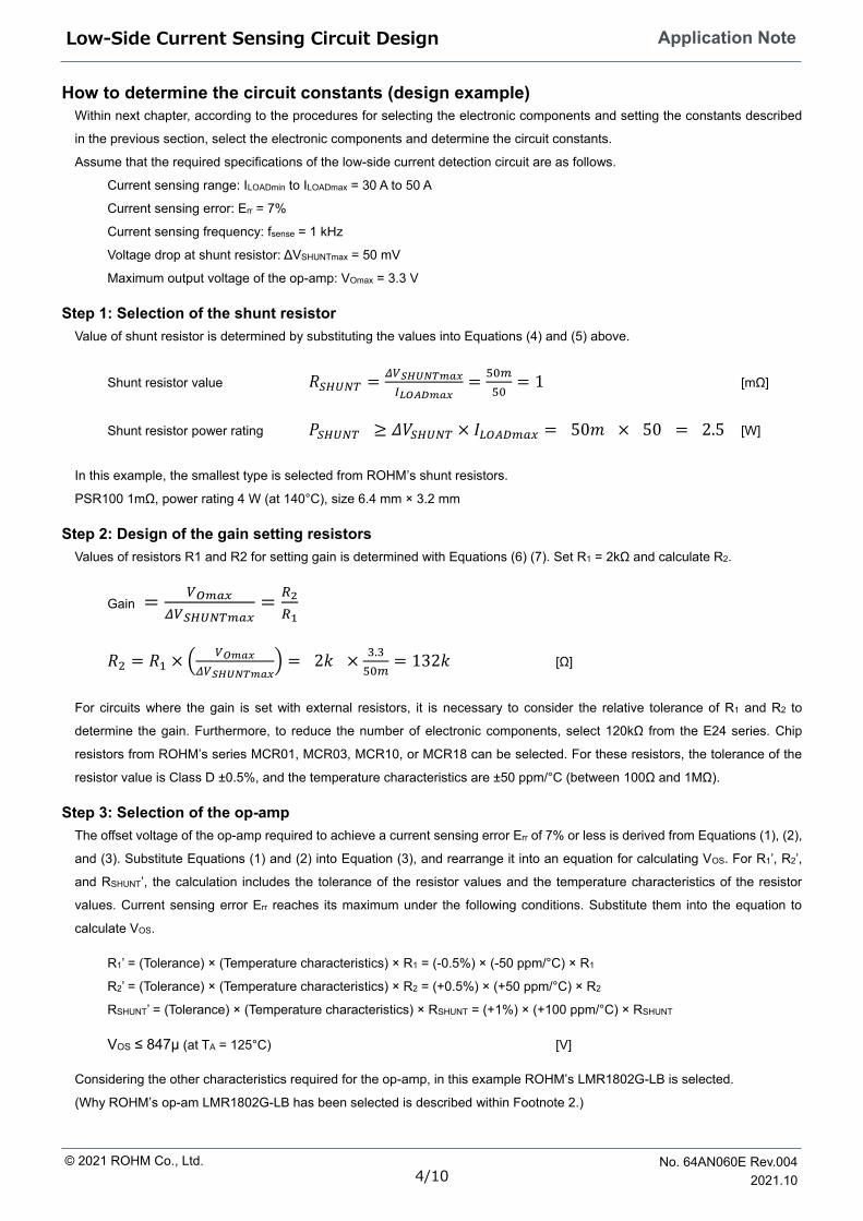
Low-Side Current Sensing Circuit Design In the areas of automotive and industrial equipment, low-side current sensing circuits are used for functions including current
(voltage) control, over current limiting, and remaining battery level detection. The low-side current sensing circuits, which are
achieved with a shunt resistor, an op-amp, and external components, can be incorporated most simply at a lower cost compared
with other methods. This application note explains the criteria for selecting parts and determining circuit constants for the low-side
current sensing circuits.
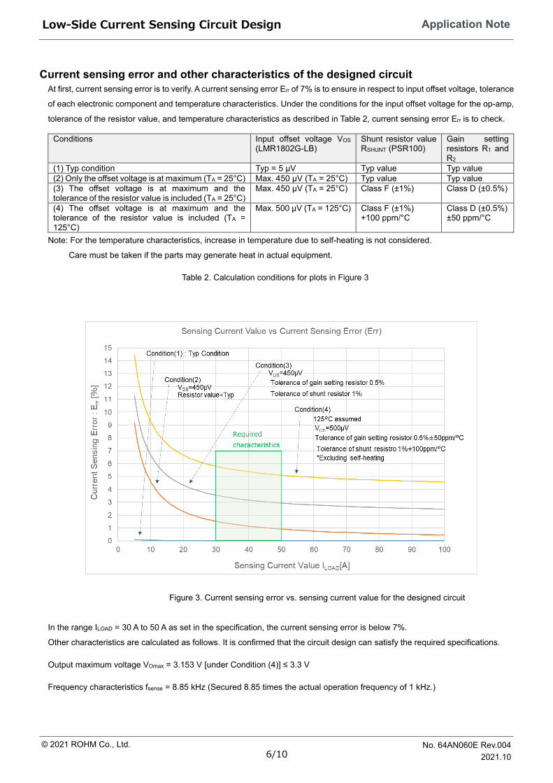
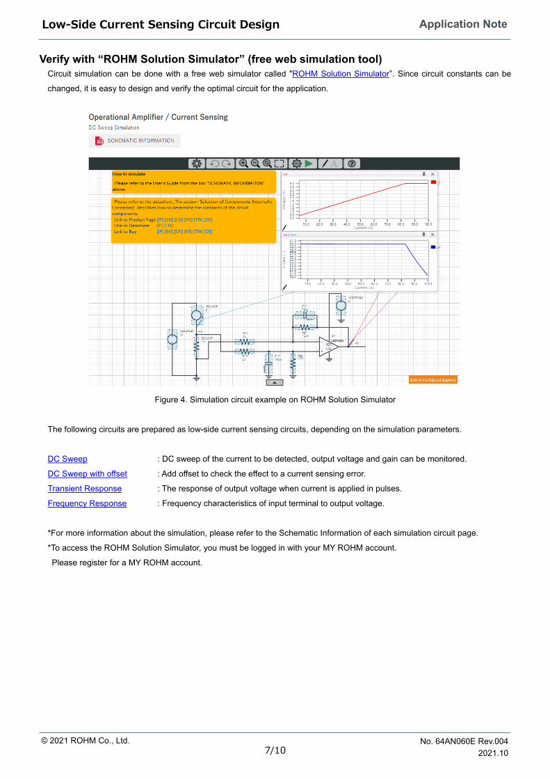
Low-side current sensing circuit
Figure 1 shows a typical low-side sensing circuit. Load current (ILOAD) from load (LOAD) via the shunt resistor (RSHUNT) causes a
voltage drop (ΔVSHUNT). This voltage is differentially amplified by the op-amp (OPAMP), connected to an A/D converter,
microcontroller, or other devices in the subsequent stage. Then, the current value is measured and used for system control.
Figure 1. Typical low-side current sensing circuit
Application Note Low-Side Current Sensing Circuit Design
Footnote2
This footnote explains characteristics of LMR1802G-LB and why this op-amp has been selected. The main characteristics of
LMR1802G-LB and the result of their examination against the required specifications are shown below.
Parameter Electrical characteristic reason for choosing LMR1802G-LG
Supply voltage range 2.5 V to 5.5 V Operable in the 3.3 V and 5 V systems.
Output voltage range VOH = VDD - VOUT: Max. 50 mV VOL: Max. 50 mV
If the input voltage range of an A/D converter or other devices in the subsequent stage is set to approximately 4 V and the op-amp is operated in the 5 V system, the circuit can be designed so that VO < 4 V.
Input voltage range Input common-mode voltage range: VSS to VDD - 1.0 V
When the op-amp is operated normally, the input voltage will be increased only to the ΔVSHUNT level at the highest, causing no issues.
Input offset voltage TA = 25°C, Typ = 5 µV Max. 500 µV over the entire temperature range
Satisfies the offset voltage specification required for the op-amp.
Note: For the detailed specifications of LMR1802G-LB, refer to the data sheet.
Table 3. Summary of the LMR1802G-LB op-amp and result of examination
The required input offset voltage range is ensured over the entire temperature range. Op-amp LMR1802G-LB was selected
because of: small temperature drift of the offset voltage (0.4 µV/°C). In power applications, heat may be generated not only by
the shunt resistor but also by peripheral circuits (for example, by a switching transistor). Therefore, it can be anticipated that
the surrounding temperature environment is undesirable. In addition, if the gain setting is relatively high, the input referred
noise voltage also emerges as an error. LMR1802G-LB has achieved an industry-leading low noise with excellent usability.
ROHM Customer Support System http://www.rohm.com/contact/
Thank you for your accessing to ROHM product informations. More detail product informations and catalogs are available, please contact us.
N o t e s
The information contained herein is subject to change without notice.
Before you use our Products, please contact our sales representative and verify the latest specifica-tions :
Although ROHM is continuously working to improve product reliability and quality, semicon-ductors can break down and malfunction due to various factors.Therefore, in order to prevent personal injury or fire arising from failure, please take safety measures such as complying with the derating characteristics, implementing redundant and fire prevention designs, and utilizing backups and fail-safe procedures. ROHM shall have no responsibility for any damages arising out of the use of our Poducts beyond the rating specified by ROHM.
Examples of application circuits, circuit constants and any other information contained herein are provided only to illustrate the standard usage and operations of the Products. The peripheral conditions must be taken into account when designing circuits for mass production.
The technical information specified herein is intended only to show the typical functions of and examples of application circuits for the Products. ROHM does not grant you, explicitly or implicitly, any license to use or exercise intellectual property or other rights held by ROHM or any other parties. ROHM shall have no responsibility whatsoever for any dispute arising out of the use of such technical information.
The Products specified in this document are not designed to be radiation tolerant.
For use of our Products in applications requiring a high degree of reliability (as exemplified below), please contact and consult with a ROHM representative : transportation equipment (i.e. cars, ships, trains), primary communication equipment, traffic lights, fire/crime prevention, safety equipment, medical systems, servers, solar cells, and power transmission systems.
Do not use our Products in applications requiring extremely high reliability, such as aerospace equipment, nuclear power control systems, and submarine repeaters.
ROHM shall have no responsibility for any damages or injury arising from non-compliance with the recommended usage conditions and specifications contained herein.
ROHM has used reasonable care to ensure the accuracy of the information contained in this document. However, ROHM does not warrants that such information is error-free, and ROHM shall have no responsibility for any damages arising from any inaccuracy or misprint of such information.
Please use the Products in accordance with any applicable environmental laws and regulations, such as the RoHS Directive. For more details, including RoHS compatibility, please contact a ROHM sales office. ROHM shall have no responsibility for any damages or losses resulting non-compliance with any applicable laws or regulations.
When providing our Products and technologies contained in this document to other countries, you must abide by the procedures and provisions stipulated in all applicable export laws and regulations, including without limitation the US Export Administration Regulations and the Foreign Exchange and Foreign Trade Act.
This document, in part or in whole, may not be reprinted or reproduced without prior consent of ROHM.