Low voltage-defect quantum cascade laser with heterogeneous injector regions
Anthony J. Hoffman1*, Stephan Schartner1,2, Scott S. Howard1, Kale J. Franz1, Fred Towner3, and Claire Gmachl1
1Department of Electrical Engineering, Princeton University, Princeton, NJ 08540, USA 2Present address: Center for Micro and Nanostructures, TU Vienna, Vienna, Austria
3 Maxion Technologies, Inc., College Park, MD 20742 Corresponding author: [email protected]
Abstract: We demonstrate an In0.635Al0.356As/In0.678Ga0.322As strain compensated quantum cascade laser that employs heterogeneous injector regions for low voltage defect operation. The active core consists of interdigitated undoped and doped injectors followed by nominally identical wavelength optical transitions. The undoped injector regions are designed with reduced voltage defect while the doped injectors are of a more conventional design. The measured average voltage defect is less than 79 meV. At 80 K, a 2.3 mm long, back facet high reflectance coated laser has an emission wavelength of 4.7 μm and outputs 2.3 W pulsed power with a peak wall-plug efficiency of 19%.
1. J. Faist, F. Capasso, D.L. Sivco, C. Sirtori, A.L. Hutchinson, and A.Y. Cho, "Quantum cascade laser," Science 264, 553 - 556 (1994).
2. M. Beck, D. Hofstetter, T. Aellen, J. Faist, U. Oesterle, M. Ilegems, E. Gini, and H. Melchior, "Continuous wave operation of a midinfrared semiconductor laser at room temperature," Science 295, 301 - 305 (2002).
3. C. Gmachl, D.L. Sivco, R. Colombelli, F. Capasso, and A.Y. Cho, "Ultra-broadband semiconductor laser," Nature 415, 883 - 887 (2002).
4. A. Tredicucci, C. Gmachl, F. Capasso, D.L. Sivco, A.L. Hutchinson, and A.Y. Cho, "A multiwavelength semiconductor laser," Nature 396, 350-353 (1998).
5. C. Gmachl, D.L. Sivco, J.N. Baillargeon, A.L. Hutchinson, F. Capasso, and A.Y. Cho, "Quantum cascade lasers with a heterogeneous cascade: Two-wavelength operation," Appl. Phys. Lett. 79, 572 - 574 (2001).
6. A. Straub, T.S. Mosely, C. Gmachl, R. Colombelli, M. Troccoli, F. Capasso, D.L. Sivco, and A.Y. Cho, "Threshold reduction in quantum cascade lasers with partially undoped, dual-wavelength interdigitated cascades," Appl. Phys. Lett. 80, 2845 -2847 (2002).
7. I. Vurgaftman and J.R. Meyer, "Analysis of limitations to wallplug efficiency and output power from quantum cascade lasers," J. Appl. Phys. 99, 123108 (2006).
8. J. Faist, "Wallplug efficiency of quantum cascade lasers: Critical parameters and fundamental limits," Appl. Phys. Lett. 90, 253512 (2007).
9. Z. Liu, Princeton University, Department of Electrical Engineering, Princeton, NJ 08544, and C. Gmachl, L. Cheng, F. Choa, F.J. Towner, X. Wang, and J. Fan have submitted a manuscript called "Temperature dependence of optical gain and loss in λ ≈ 8.2 - 10.2 μm quantum cascade lasers," to IEEE J. Quantum Elect.
10. J. Nguyen, J.S. Yu, A. Evans, S. Slivken, and M. Razeghi, "Optical coatings by ion-beam sputtering deposition for long-wave infrared quantum cascade lasers," Appl. Phys. Lett. 89, 111113 (2006).
11. A. Tsekoun, R. Go, M. Pushkarsky, M. Razeghi, and C.K.N. Patel, "Improved performance of quantum cascade lasers through a scalable, manufacturable epitaxial-side-down mountin process," PNAS 103, 4831 - 4835 (2006).
12. A. Evans, S.R. Darvish, S. Slivken, J. Nguyen, Y. Bai, and M. Razeghi, "Buried heterostructure quantum cascade lasers with high continuous-wave wall plug efficiency," Appl. Phys. Lett. 91, 071101 (2007).
13. J.S. Yu, S.R. Darvish, A. Evans, J. Nguyen, S. Slivken, and M. Razeghi, "Room-temperature continuous-wave operation of quantum-cascade lasers at λ ~ 4 μm " Appl. Phys. Lett. 88, 041111 (2006).
#88010 - $15.00 USD Received 28 Sep 2007; revised 5 Nov 2007; accepted 7 Nov 2007; published 14 Nov 2007
(C) 2007 OSA 26 November 2007 / Vol. 15, No. 24 / OPTICS EXPRESS 15818
14. A. Evans, J.S. Yu, J. David, L. Doris, K. Mi, S. Slivken, and M. Razeghi, "High-temperature, high-power, continuous-wave operation of buried heterostructure quantum-cascade lasers," Appl. Phys. Lett. 84, 314 - 316 (2004).
15. A. Evans, J.S. Yu, S. Slivken, and M. Razeghi, "Continuous-wave operation of λ ~ 4.8 μm quantum-cascade lasers at room temperature," Appl. Phys. Lett. 85, 2166 -2168 (2004).
1. Introduction
Since the first demonstration of the quantum cascade (QC) laser [1], several devices have been developed that exhibit desirable characteristics such as room temperature continuous wave operation, broad tuning, and multiple wavelength emission [2-4]. These advances are all possible because of the large design space inherent in the lasers which allows the optimization of the active laser core for a particular objective. An example of this flexibility is heterogeneous active region QC lasers, in which the active core consists of stacked or alternating different active regions [5, 6]. In this paper, we apply the notion of design optimization through heterogeneous injector regions to the wall-plug efficiency (WPE).
From a technological and commercial perspective, QC lasers that operate with high WPE are very desirable; yet, improving this parameter has only recently received much attention. Strategies to increase the WPE can be separated into two main categories. The first focuses on maximizing the WPE for a given active core design and has been addressed on several fronts. As shown theoretically [7, 8], moderate reductions in the waveguide loss of QC lasers can lead to significant performance improvements, and effort is being put forth to understand the loss mechanisms in these lasers [9]. Additionally, high reflection and anti-reflection coatings applied to opposite facets of a QC laser have also resulted in improved WPE [10]. Finally, improved thermal management through device geometery, high quality growth, epilayer-side mounting, and buried heterostructure regrowth, has also proven to be a viable strategy [11-14]. The second category focuses on improving the quantum design of the active QC laser core. While most of the parameters that maximize the WPE are closely linked with those that maximize output power and result in high performance operation, the design of the active core has yet to take full advantage of the substantial design space. Here, we present a QC laser that adapts the idea of a heterogeneous design and applies it to the injector regions rather than the light generating active regions. For this laser, conventional, doped injectors and novel, undoped injectors with reduced voltage defect are alternated between two different active regions with nominally identical transition energies. The second injector design is used to reduce the voltage drop in the active core that does not contribute to the optical power generated by the laser. For comparison, a conventional QC laser has a voltage defect of approximately 140 meV [12, 15], while the laser reported here has an average voltage defect of less than 79 meV (i.e. about half of the conventional design). For our active core, reducing the voltage defect from 140 meV to 79 meV, leads to an estimated increase in the WPE of an additional 10 %.
2. Laser design and fabrication
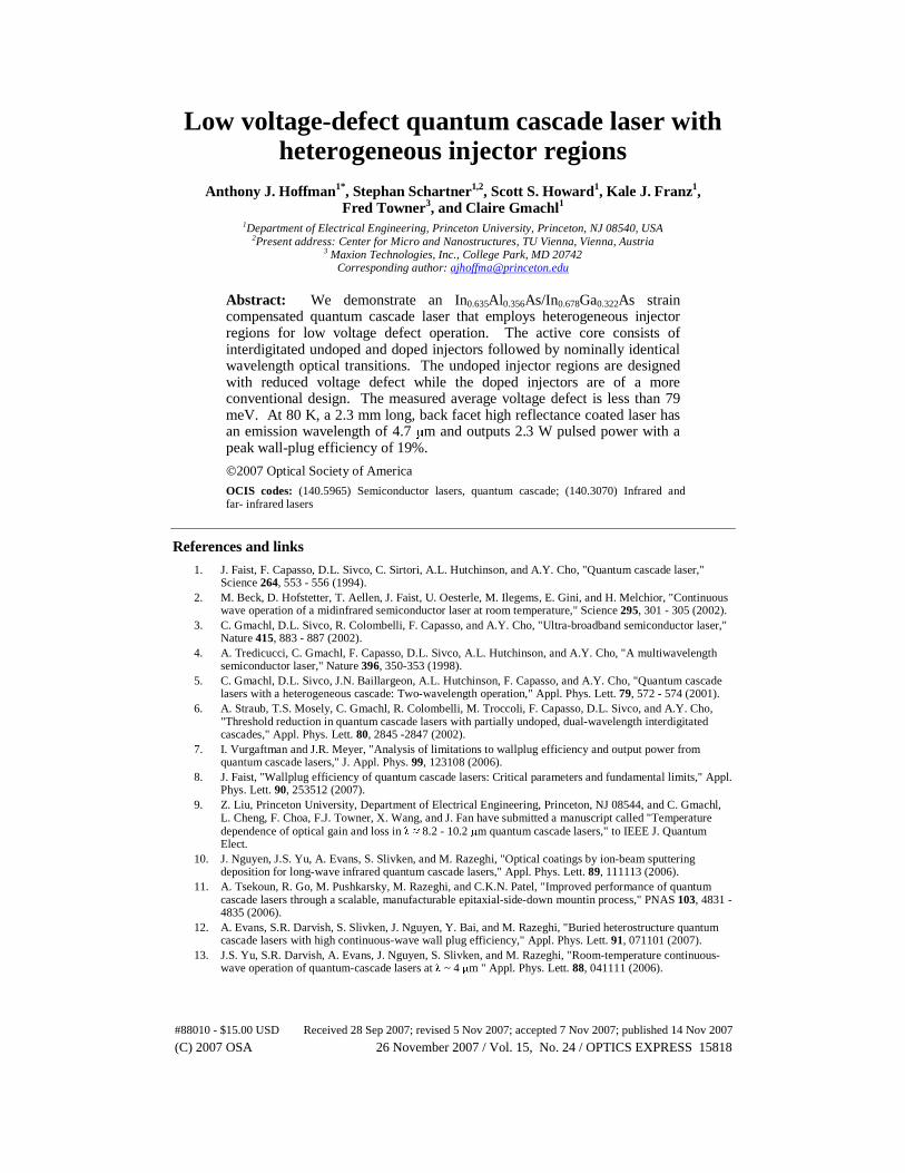
A portion of the conduction band of the QC laser is shown in Fig. 1. The active core is composed of two optical transitions with identical energies preceded by alternating doped and undoped injector regions. The layer sequence in angstroms of one period starting with the extraction barrier labeled “*” is 25/29/18/24/19/23/21/21/27/20/39/52/13/40/22/33/18/29/19/ 26/21/21/25/20/27/19/38/13/15/44/13/40/13/34 where In0.635Al0.356As barrier layers are in bold, In0.678Ga0.322As well layers in times roman font, and the n-doped (4.4x1017 cm-3) layers are underlined. The first injector region, labeled A in Fig 1, is a conventional, doped injector that is optimized for both voltage defect (shaded in green) and electron extraction from the previous transition. The active region following this injector employs a single phonon resonance to empty the lower laser level of electrons; the transition has a design energy of 283 meV. The second injector, B, is undoped and is designed to minimize the voltage defect (shaded in blue) while still providing fast electron extraction. The active region following this
#88010 - $15.00 USD Received 28 Sep 2007; revised 5 Nov 2007; accepted 7 Nov 2007; published 14 Nov 2007
(C) 2007 OSA 26 November 2007 / Vol. 15, No. 24 / OPTICS EXPRESS 15819
injector is a double-phonon resonance design with the same nominal transition energy as the previous active region. A consequence of the low energy drop injector design in this laser is that three states are mixed in the upper-level of the active region following the injector. In conventional designs, typically only two states mix and thus larger than normal broadening of the gain spectrum is expected.
Fig. 1. A portion of the conduction band structure with the moduli squared of the relevant wavefunctions. The optical transitions with design energies of 283 meV are denoted by the vertical black arrows. The doped and undoped injector regions are marked by the letters A and B, respectively. The shaded green and blue regions in the band diagram show the voltage defect for the two injectors. The extraction barrier marked “*”, indicates the first barrier for the design sequence detailed in the main text. The calculation is for an applied electric field of 82 kV/cm.
The laser was grown by molecular beam epitaxy (MBE) on low-doped (n ~ 1x1017 cm-3)
InP substrate using strain-compensated Al0.635In0.365As/In0.678Ga0.322As. The doped injector–first active region–undoped injector–second active region sequence was repeated 17 times and sandwiched between two 0.17 μm thick n-doped (5x1016 cm-3) lattice-matched InGaAs layers for enhanced optical waveguide confinement. Additional upper cladding layers of 2.7 μm InP (1x1017 cm-3) and 0.4 μm InP (8x1018 cm-3) were grown above the top InGaAs layer before a final 100 Å thick layer of InP (1x1019 cm-3). The waveguide has a calculated confinement factor of Γ = 70%
The wafer was processed into semicircular mesas for electroluminescence (EL) measurements and into deep-etched ridge waveguide lasers. The mesas were wet etched and ~200 μm in diameter. The sample was thinned to ~200 μm and Ti/Au (250/2500 Å) top contacts and Ge/Au (250/2500 Å) back-side contacts were deposited. The mesas were cleaved approximately along the diameter and mounted to a copper heat sink. The ridge waveguide lasers were processed using conventional wet-chemical techniques. The ridge widths varied from 12 to 23 μm, 3300 Å of SixNy was used for side-wall insulation and Ti/Au (250/2500 Å) was used for top contacts. The InP substrate was thinned to ~200 μm, Ge/Au (250 Å /2500 Å) was deposited for back-side contacts, and the lasers were mounted epilayer-up to a copper heat sink with In solder. After the initial characterization, the back facet of several lasers was high-reflection (HR) coated with SiO2/Ti/Au/SiO2 (4000/150/1500/1000 Å).
3. Experimental results and discussion
Pulsed EL measurements were carried out on the cleaved mesas using a Fourier transform infrared (FTIR) spectrometer and a cooled HgCdTe detector. The lasers were mounted to the cold finger of a continuous flow liquid nitrogen cryostat. Pulses of various widths (100 ns to 4 μs) with a 79.9 kHz repetition rate were used. Spectral measurements were recorded from 80 K to room temperature for a large range of applied electric current and are shown in
#88010 - $15.00 USD Received 28 Sep 2007; revised 5 Nov 2007; accepted 7 Nov 2007; published 14 Nov 2007
(C) 2007 OSA 26 November 2007 / Vol. 15, No. 24 / OPTICS EXPRESS 15820
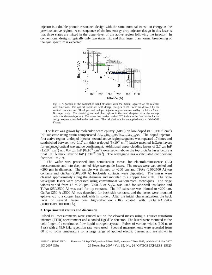
Fig. 2(a) for 80 K. The inset of the figure shows a current-voltage curve for the device at 80 K. Despite the active core containing two different active region designs, the EL data closely resembles that of a homogeneous design QC laser.
For further inspection, the EL spectra were fit using a nonlinear regression with two Lorentzian functions; a characteristic fit is shown in the inset of Fig 2(b). The spectral position of the peak and the full width at half maximum (FWHM) were determined for each Lorentzian and are shown in Fig. 2(b). The two peak positions tune similarly with applied field and are attributed to the two primary optical transitions shown in Fig. 1. Over the range of applied fields, the spectral positions of the two peaks differ by approximately 10 meV. The higher energy transition (represented by black data points), which we attribute to luminescence from the active region following the doped injector region, has a full width at half maximum around 14 meV and varies by a few percent over the range of applied electric fields. The lower energy luminescence peak (represented by red data) corresponding to light generated from the active region following the undoped injector region has a FWHM that varies by more than 10% and is approximately 10 meV broader than the higher energy peak. The broader transition and the stronger influence of the applied field are attributed to the multiple states that compose the upper-laser level as seen in Fig. 1.
Fig. 2. (a). Pulsed EL spectra at 80 K from cleaved mesas as a function of current. Various pulse widths, 100 ns to 4 μs, at a repetition rate of 79.9 kHz were used for the measurements. The inset shows a current-voltage plot for the same device at 80 K. (b) Spectral peak position (squares) and full width at half maximum (circles) of the fit Lorentzians versus applied current. The red data points are attributed to optical transitions following the undoped injectors and the black data points are attributed to optical transitions following the conventional injectors. The inset shows a characteristic double-peak Lorentzian fit of an EL spectrum.
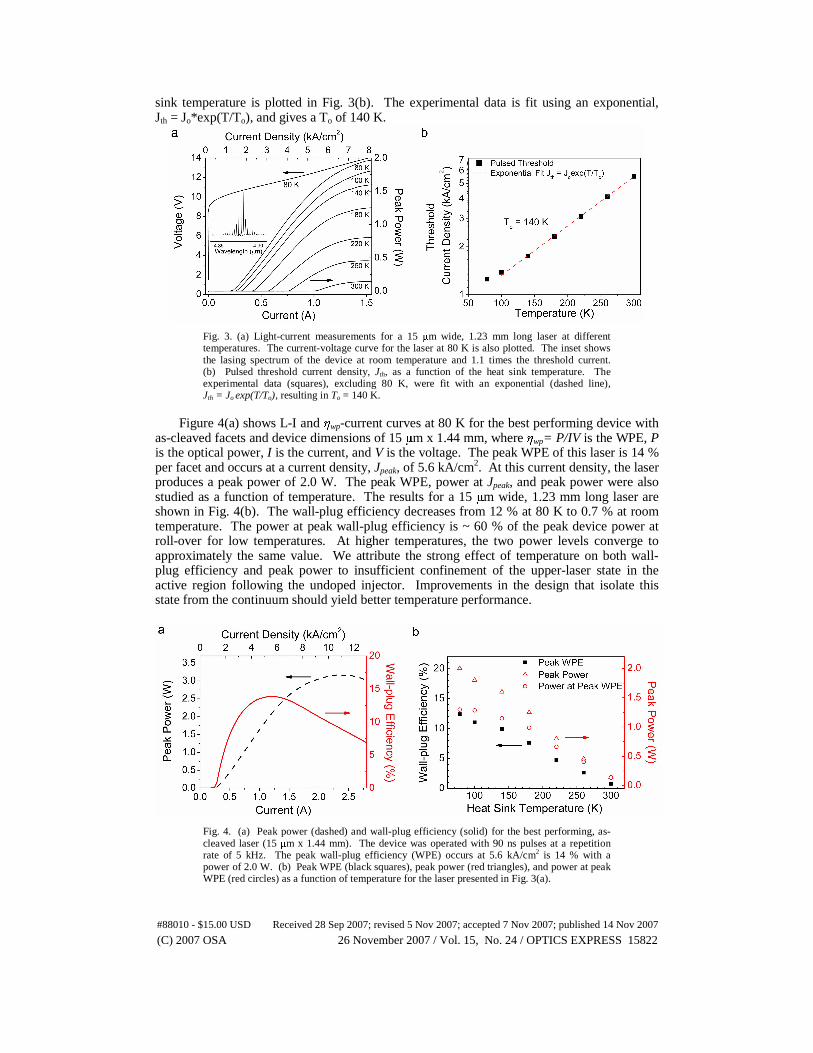
Light-current-voltage (LIV) measurements were performed on many lasers of various
ridge widths and cavity lengths. Measurements were performed in pulsed mode operation using 90 ns pulses with a repetition rate of 5 kHz and a room temperature HgCdTe detector. Power measurements were calibrated using a pyrometer detector. A gated integrator and boxcar averager with a 20 ns gate width was used to sample LIV pulses. Figure 3(a) shows characteristic LI data as a function of temperature for a 1.23 mm long, 15 μm wide laser. The current-voltage curve for 80 K is also plotted. At 80 K, a peak power of 2.0 W was obtained with a threshold current density of 1.2 kA/cm2. The emission wavelength is centered at 4.70 μm at 80 K and increases to 4.88 μm at 300 K. The room temperature spectrum of the device at 10 % above threshold current is shown in the inset of Fig. 3(a). Using IV data at 80 K for several lasers and assuming the entire voltage drop occurs over the active core, a voltage defect of 79 meV per injector-active region pair is calculated. Allowing for 0.25 V drop due to contact and waveguide resistance [7], a voltage defect of 71 meV per injector-active region pair is extracted. Calculations using the design bandstructure predict a value of 71 meV averaged per injector-active region pair. Threshold current density, Jth, as a function of heat
#88010 - $15.00 USD Received 28 Sep 2007; revised 5 Nov 2007; accepted 7 Nov 2007; published 14 Nov 2007
(C) 2007 OSA 26 November 2007 / Vol. 15, No. 24 / OPTICS EXPRESS 15821
sink temperature is plotted in Fig. 3(b). The experimental data is fit using an exponential, Jth = Jo*exp(T/To), and gives a To of 140 K.
Fig. 3. (a) Light-current measurements for a 15 μm wide, 1.23 mm long laser at different temperatures. The current-voltage curve for the laser at 80 K is also plotted. The inset shows the lasing spectrum of the device at room temperature and 1.1 times the threshold current. (b) Pulsed threshold current density, Jth, as a function of the heat sink temperature. The experimental data (squares), excluding 80 K, were fit with an exponential (dashed line), Jth = Jo exp(T/To), resulting in To = 140 K.
Figure 4(a) shows L-I and ηwp-current curves at 80 K for the best performing device with
as-cleaved facets and device dimensions of 15 μm x 1.44 mm, where ηwp= P/IV is the WPE, P is the optical power, I is the current, and V is the voltage. The peak WPE of this laser is 14 % per facet and occurs at a current density, Jpeak, of 5.6 kA/cm2. At this current density, the laser produces a peak power of 2.0 W. The peak WPE, power at Jpeak, and peak power were also studied as a function of temperature. The results for a 15 μm wide, 1.23 mm long laser are shown in Fig. 4(b). The wall-plug efficiency decreases from 12 % at 80 K to 0.7 % at room temperature. The power at peak wall-plug efficiency is ~ 60 % of the peak device power at roll-over for low temperatures. At higher temperatures, the two power levels converge to approximately the same value. We attribute the strong effect of temperature on both wall-plug efficiency and peak power to insufficient confinement of the upper-laser state in the active region following the undoped injector. Improvements in the design that isolate this state from the continuum should yield better temperature performance.
Fig. 4. (a) Peak power (dashed) and wall-plug efficiency (solid) for the best performing, as-cleaved laser (15 μm x 1.44 mm). The device was operated with 90 ns pulses at a repetition rate of 5 kHz. The peak wall-plug efficiency (WPE) occurs at 5.6 kA/cm2 is 14 % with a power of 2.0 W. (b) Peak WPE (black squares), peak power (red triangles), and power at peak WPE (red circles) as a function of temperature for the laser presented in Fig. 3(a).
#88010 - $15.00 USD Received 28 Sep 2007; revised 5 Nov 2007; accepted 7 Nov 2007; published 14 Nov 2007
(C) 2007 OSA 26 November 2007 / Vol. 15, No. 24 / OPTICS EXPRESS 15822
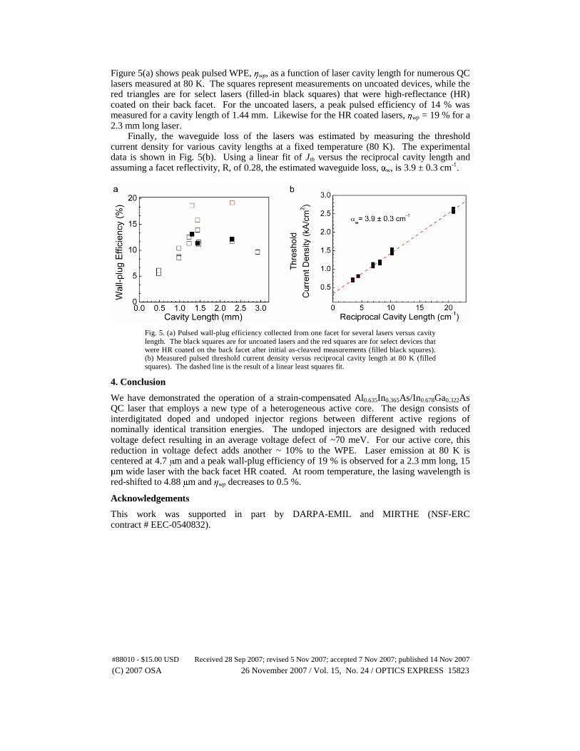
Figure 5(a) shows peak pulsed WPE, ηwp, as a function of laser cavity length for numerous QC lasers measured at 80 K. The squares represent measurements on uncoated devices, while the red triangles are for select lasers (filled-in black squares) that were high-reflectance (HR) coated on their back facet. For the uncoated lasers, a peak pulsed efficiency of 14 % was measured for a cavity length of 1.44 mm. Likewise for the HR coated lasers, ηwp = 19 % for a 2.3 mm long laser.
Finally, the waveguide loss of the lasers was estimated by measuring the threshold current density for various cavity lengths at a fixed temperature (80 K). The experimental data is shown in Fig. 5(b). Using a linear fit of Jth versus the reciprocal cavity length and assuming a facet reflectivity, R, of 0.28, the estimated waveguide loss, αw, is 3.9 ± 0.3 cm-1.
Fig. 5. (a) Pulsed wall-plug efficiency collected from one facet for several lasers versus cavity length. The black squares are for uncoated lasers and the red squares are for select devices that were HR coated on the back facet after initial as-cleaved measurements (filled black squares). (b) Measured pulsed threshold current density versus reciprocal cavity length at 80 K (filled squares). The dashed line is the result of a linear least squares fit.
4. Conclusion
We have demonstrated the operation of a strain-compensated Al0.635In0.365As/In0.678Ga0.322As QC laser that employs a new type of a heterogeneous active core. The design consists of interdigitated doped and undoped injector regions between different active regions of nominally identical transition energies. The undoped injectors are designed with reduced voltage defect resulting in an average voltage defect of ~70 meV. For our active core, this reduction in voltage defect adds another ~ 10% to the WPE. Laser emission at 80 K is centered at 4.7 μm and a peak wall-plug efficiency of 19 % is observed for a 2.3 mm long, 15 μm wide laser with the back facet HR coated. At room temperature, the lasing wavelength is red-shifted to 4.88 μm and ηwp decreases to 0.5 %.
Acknowledgements
This work was supported in part by DARPA-EMIL and MIRTHE (NSF-ERC contract # EEC-0540832).
#88010 - $15.00 USD Received 28 Sep 2007; revised 5 Nov 2007; accepted 7 Nov 2007; published 14 Nov 2007
(C) 2007 OSA 26 November 2007 / Vol. 15, No. 24 / OPTICS EXPRESS 15823