Low voltage, high performance inkjet printed carbon nanotube transistors with solution processed ZrO2 gate insulator Bongjun Kim, Seonpil Jang, Pradyumna L. Prabhumirashi, Michael L. Geier, Mark C. Hersam, and Ananth Dodabalapur Citation: Applied Physics Letters 103, 082119 (2013); doi: 10.1063/1.4819465 View online: http://dx.doi.org/10.1063/1.4819465 View Table of Contents: http://scitation.aip.org/content/aip/journal/apl/103/8?ver=pdfcov Published by the AIP Publishing Articles you may be interested in High performance transistors via aligned polyfluorene-sorted carbon nanotubes Appl. Phys. Lett. 104, 083107 (2014); 10.1063/1.4866577 Inkjet printed ambipolar transistors and inverters based on carbon nanotube/zinc tin oxide heterostructures Appl. Phys. Lett. 104, 062101 (2014); 10.1063/1.4864629 All-printed and transparent single walled carbon nanotube thin film transistor devices Appl. Phys. Lett. 103, 143303 (2013); 10.1063/1.4824475 Solution processable carbon nanotube network thin-film transistors operated in electrolytic solutions at various pH Appl. Phys. Lett. 101, 223101 (2012); 10.1063/1.4768683 High-frequency performance of scaled carbon nanotube array field-effect transistors Appl. Phys. Lett. 101, 053123 (2012); 10.1063/1.4742325 This article is copyrighted as indicated in the article. Reuse of AIP content is subject to the terms at: http://scitation.aip.org/termsconditions. Downloaded to IP: 137.30.242.61 On: Mon, 07 Jul 2014 02:00:20
Transcript
Low voltage, high performance inkjet printed carbon nanotube transistors with solutionprocessed ZrO2 gate insulatorBongjun Kim, Seonpil Jang, Pradyumna L. Prabhumirashi, Michael L. Geier, Mark C. Hersam, and Ananth
Dodabalapur
Citation: Applied Physics Letters 103, 082119 (2013); doi: 10.1063/1.4819465 View online: http://dx.doi.org/10.1063/1.4819465 View Table of Contents: http://scitation.aip.org/content/aip/journal/apl/103/8?ver=pdfcov Published by the AIP Publishing Articles you may be interested in High performance transistors via aligned polyfluorene-sorted carbon nanotubes Appl. Phys. Lett. 104, 083107 (2014); 10.1063/1.4866577 Inkjet printed ambipolar transistors and inverters based on carbon nanotube/zinc tin oxide heterostructures Appl. Phys. Lett. 104, 062101 (2014); 10.1063/1.4864629 All-printed and transparent single walled carbon nanotube thin film transistor devices Appl. Phys. Lett. 103, 143303 (2013); 10.1063/1.4824475 Solution processable carbon nanotube network thin-film transistors operated in electrolytic solutions at variouspH Appl. Phys. Lett. 101, 223101 (2012); 10.1063/1.4768683 High-frequency performance of scaled carbon nanotube array field-effect transistors Appl. Phys. Lett. 101, 053123 (2012); 10.1063/1.4742325
This article is copyrighted as indicated in the article. Reuse of AIP content is subject to the terms at: http://scitation.aip.org/termsconditions. Downloaded to IP:
Low voltage, high performance inkjet printed carbon nanotubetransistors with solution processed ZrO2 gate insulator
Bongjun Kim,1,2 Seonpil Jang,1,2 Pradyumna L. Prabhumirashi,3 Michael L. Geier,3
Mark C. Hersam,3,4,5,a) and Ananth Dodabalapur1,2,b)
1Microelectronics Research Center, The University of Texas at Austin, Austin, Texas 78758, USA2Department of Electrical and Computer Engineering, The University of Texas at Austin, Austin, Texas 78712,USA3Department of Materials Science and Engineering, Northwestern University, Evanston, Illinois 60208, USA4Department of Chemistry, Northwestern University, Evanston, Illinois 60208, USA5Department of Medicine, Northwestern University, Evanston, Illinois 60208, USA
(Received 31 July 2013; accepted 8 August 2013; published online 23 August 2013)
High-performance single-walled carbon nanotube (SWCNT) thin-film transistors are fabricated by
single-pass inkjet printing of SWCNTs on high-j solution-processed ZrO2 gate dielectric. We
demonstrate that an ultraviolet ozone treatment of the ZrO2 substrate is critical in achieving a
uniform dispersion of sorted SWCNTs in the semiconducting channel. The resulting devices exhibit
excellent performance with mobility and on/off current ratio exceeding 30 cm2 V�1 s�1 and 105,
respectively, at low operating voltages (<5 V). The single-pass inkjet printing process demonstrated
in this letter shows great promise as a reliable and scalable method for SWCNT based high
This article is copyrighted as indicated in the article. Reuse of AIP content is subject to the terms at: http://scitation.aip.org/termsconditions. Downloaded to IP:
The SWCNT ink was then dialyzed (Slide-A-Lyzer Dialysis
Cassettes, 20 K MWCO, 0.5 ml, Pierce Biotechnology, Inc.)
into 1% w v�1 sodium cholate aqueous solution in order to
remove the density gradient medium (iodixanol). After dialy-
sis, the high-purity semiconducting ink was subsequently used
to fabricate a SWCNT buckypaper via vacuum filtration
through a porous nylon membrane (Whatman WNYL,
0.2 lm), followed by copious rinsing with nanopure water
(18.2 MX-cm resistivity) to remove surfactants from the
SWCNTs. Once dry, the SWCNT buckypaper was first dis-
persed in 1-cyclohexyl-2-pyrrolidone (CHP) and then ultra-
sonicated in a bath-type ultrasonic cleaner for 6 h to make a
uniform suspension. The concentration of SWCNTs in the ink
was 0.1 mg ml�1. Before inkjet printing, the ink was ultrasoni-
cated again for more than 2 h to form a uniform dispersion of
SWCNTs in CHP.
The SWCNT TFT fabrication process is illustrated in
Figure 1. A high-j dielectric, ZrO2, was deposited on a heav-
ily doped Si wafer by a sol-gel route.27 After the deposition
of ZrO2, source and drain (S/D) electrodes consisting of a Ti/
Au (3 nm/30 nm) double layer were deposited by thermal
evaporation followed by the lift-off process. Following this
step, the dielectric surface was exposed to UV light in air for
10 min. The SWCNT ink (with >98% semiconducting
SWCNTs) was inkjet printed on UV O3 treated ZrO2 using a
Fuji Dimatix 2800 printer at room temperature in air. After
printing, the ink was dried on a hotplate at 200 �C for 30 min
in air to remove residual solvents.
Figure 2(a) shows an optical image of the SWCNT TFT
array. The array has several TFTs possessing different chan-
nel lengths, L (varying from 20 lm to 250 lm), and channel
width, W (W/L¼ 20). Figure 2(b) shows the low-
magnification scanning electron micrograph of a SWCNT
TFT with L of 150 lm and W of 3000 lm. Figure 2(c) is a
higher magnification scanning electron micrograph display-
ing dense and uniform networks of SWCNTs in the channel.
Figure 2(d) shows the optical absorbance spectra for sorted
semiconducting and unsorted SWCNTs, respectively. The
purity of the SWCNTs is determined to be >98% by com-
paring the areas under the metallic (M11) and semiconduct-
ing (S22) optical transitions.
Uniformly distributed networks of SWCNTs are essential
to obtain high-performance TFTs. Sparse networks of
SWCNTs cannot transport carriers effectively and thick
SWCNT bundles can cause high OFF currents due to poor
gate control as a consequence of tube to tube screening. In our
SWCNT TFT structures, UV O3 treatment was applied to the
ZrO2 surface to promote the wetting of the SWCNT ink by
rendering the surface hydrophilic.28 To observe the effect of
UV O3 treatment on solution processed ZrO2, the contact
angle formed by H2O and ethylene glycol drops on ZrO2 was
measured before and after the treatment. The surface energy,
calculated using measured contact angles, increased by �60%
(from 48.3 mJ m�2 to 75.9 mJ m�2) after the UV O3 treat-
ment. This indicates that the UV O3 treatment changed the
conditions of the ZrO2 surface to make it hydrophilic, which
helps the SWCNT ink wet the surface uniformly.
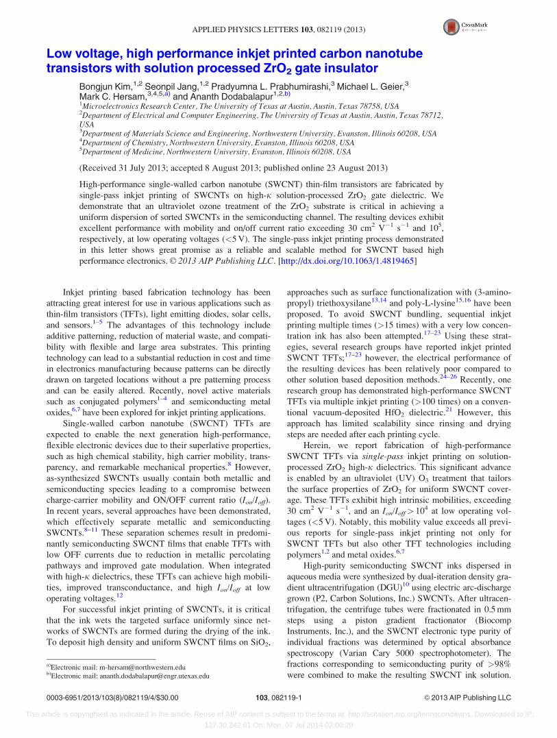
Figures 3(a) and 3(b) show the atomic force microscopy
(AFM) images of the inkjet printed SWCNT network on
untreated and UV O3 treated ZrO2, respectively. It can be
clearly observed that significant areas remain uncovered
(with SWCNTs) on pristine ZrO2, Figure 3(a). After the
UV O3 treatment, inkjet printed SWCNT film coverage is
uniform and densely distributed as shown in Figure 3(b).
Figure 3(c) displays the substantial difference in transfer
characteristics between UV O3 treated and untreated devices.
The gate modulation of the channel current in the UV O3
treated devices is strong, with an Ion/Ioff of 9.1� 104,
whereas in the untreated device there is very little gate mod-
ulation of the drain current. This gate-voltage-independent
high current in the untreated devices may be due to the
aggregation of SWCNTs in thick bundles resulting in very
poor gate control due to screening.
The TFT measurements were performed in ambient
conditions using an HP 4155 C semiconductor parameterFIG. 1. The process of inkjet printed SWCNT TFT fabrication.
FIG. 2. (a) Optical image of the SWCNT TFT array. (b) Low-magnification
SEM image of a SWCNT TFT (L¼ 150 lm, W¼ 3000 lm). (c) SEM image
of SWCNT distribution in the channel area (red square in (b)). (d) Optical
absorbance spectra of the SWCNT ink.
082119-2 Kim et al. Appl. Phys. Lett. 103, 082119 (2013)
This article is copyrighted as indicated in the article. Reuse of AIP content is subject to the terms at: http://scitation.aip.org/termsconditions. Downloaded to IP:
137.30.242.61 On: Mon, 07 Jul 2014 02:00:20
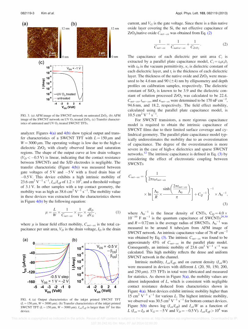
analyzer. Figures 4(a) and 4(b) show typical output and trans-
fer characteristics of a SWCNT TFT with L¼ 150 lm and
W¼ 3000 lm. The operating voltage is low due to the high-jdielectric ZrO2 with clearly observed linear and saturation
regions. The shape of the output curve at low drain voltages
(VD<�0.5 V) is linear, indicating that the contact resistance
between SWCNTs and the S/D electrodes is negligible. The
transfer characteristic (Figure 4(b)) was measured between
gate voltages of 5 V and �5 V with a fixed drain bias of
�0.5 V. This device exhibits a high intrinsic mobility of
23.6 cm2 V�1 s�1, Ion/Ioff of 1.2� 105, and a threshold voltage
of 3.1 V. In other samples with a top contact geometry, the
mobility was as high as 38.6 cm2 V�1 s�1. The mobility value
in these devices was extracted from the characteristics shown
in Figure 4(b) by the following equation:
l ¼ L
W� 1
Cnet�ox� 1
VD� dID
dVG; (1)
where l is linear field effect mobility, Cnet�ox is the total ca-
pacitance per unit area, VD is the drain voltage, ID is the drain
current, and VG is the gate voltage. Since there is a thin native
oxide layer covering the Si, the net effective capacitance of
ZrO2/native oxide Cnet�ox was obtained from Eq. (2)
1
Cnet�ox¼ 1
Cnative�oxþ 1
CZrO2
: (2)
The capacitance of each dielectric per unit area Ci is
extracted by a parallel plate capacitance model, Ci¼ e0ji/tiwith e0 is the vacuum permittivity, ji is dielectric constant of
each dielectric layer, and ti is the thickness of each dielectric
layer. The thickness of the native oxide and ZrO2 were meas-
ured to be 4.6 nm and 90 (64) nm by ellipsometry and depth
profiles on calibration samples, respectively. The dielectric
constant of SiO2 is known to be 3.9 and the dielectric con-
stant of solution processed ZrO2 was calculated to be 22.4.
Cnet�ox, tnet�ox, and jnet�ox were determined to be 170 nF cm�2,
94.6 nm, and 18.2, respectively. The field effect mobility,
calculated using the parallel plate capacitance model, is
10.5 cm2 V�1 s�1.
For SWCNT transistors, a more rigorous capacitance
model is required to obtain the intrinsic capacitance of
SWCNT films due to their limited surface coverage and cy-
lindrical geometry. The parallel plate capacitance model typ-
ically underestimates the mobility due to an overestimation
of capacitance. The degree of the overestimation is more
severe in the case of high-j dielectrics and sparse SWCNT
networks.12 The intrinsic capacitance is defined in Eq. (3) by
considering the effect of electrostatic coupling between
SWCNTs
Cnet�ox ¼(
1
2pe0enet�ox
� ln
"K0
R�
sinh
�2ptnet�ox
K0
�p
#þCQ
�1
)�1
�K0�1;
(3)
where K0�1 is the linear density of CNTs, CQ¼ 4.0�
10�10 F m�1 is the quantum capacitance of SWCNTs29,30
and R¼ 0.72 nm is the average radius of SWCNTs. K0�1 was
measured to be around 8 tubes/lm from AFM image of
SWCNT network. An intrinsic capacitance value of 76 nF cm�2
was obtained by Eq. (3). The intrinsic Cnet�ox was found to be
approximately 45% of Cnet�ox in the parallel plate model.
Consequently, an intrinsic mobility of 23.6 cm2 V�1 s�1 was
calculated. This high mobility reflects the dense and uniform
SWCNT network in the channel.
Intrinsic mobility, Ion/Ioff, and on current density (Ion/W)
were measured in devices with different L (20, 50, 150, 200,
and 250 lm). 375 TFTs in total were fabricated and measured
for statistics. As shown in Figure 5(a), the mobility values are
almost independent of L, which is consistent with negligible
contact resistance deduced from characteristics shown in
Figure 4(a). Most devices exhibit intrinsic mobility higher than
15 cm2 V�1 s�1 for various L. The highest intrinsic mobility,
we observed was 30.5 cm2 V�1 s�1 for bottom contact devices.
Figure 5(b) shows log (Ion/Ioff) and Ion/W as a function of
L (Ion¼ ID at VG¼�5 V and VD¼�0.5 V). Ion/Ioff> 104 was
FIG. 3. (a) AFM image of the SWCNT network on untreated ZrO2. (b) AFM
image of the SWCNT network on UV O3 treated ZrO2. (c) Transfer character-
istics of untreated and UV O3 treated SWCNT TFTs.
FIG. 4. (a) Output characteristics of the inkjet printed SWCNT TFT
(L¼ 150 lm, W¼ 3000 lm). (b) Transfer characteristics of the inkjet printed
SWCNT TFT (L¼ 150 lm, W¼ 3000 lm). Ion/Ioff is larger than 105 for this
device.
082119-3 Kim et al. Appl. Phys. Lett. 103, 082119 (2013)
This article is copyrighted as indicated in the article. Reuse of AIP content is subject to the terms at: http://scitation.aip.org/termsconditions. Downloaded to IP:
137.30.242.61 On: Mon, 07 Jul 2014 02:00:20
observed in most devices for various L. The highest Ion/Ioff, we
observed was 7.4� 106. The mobility, we report in this paper,
is more than an order of magnitude higher than the best
reported values for TFTs with inkjet printed conjugated poly-
mers1,2 and is also higher than those reported for inkjet printed
metal oxides.6,7
In conclusion, we have demonstrated high performance
SWCNT TFTs with mobilities exceeding 30 cm2 V�1 s�1 and
low operating voltages by single-pass inkjet printing of
SWCNTs on high-j ZrO2. The high mobilities achieved in
this work show that sorted SWCNTs are a promising alterna-
tive to polymers and semiconducting oxides for inkjet printing
based fabrication. Surface energy modification of the ZrO2
surface is the key to the realization of uniform and dense net-
works of SWCNTs. The single-pass inkjet printing process
demonstrated in this letter, combined with solution processed
ZrO2, shows great promise as a reliable and scalable method
for high performance flexible electronics applications.
The authors acknowledge financial support from the
Office of Naval Research MURI Grant No. # N00014-11-1-
0690. A National Science Foundation Graduate Research
Fellowship (M.L.G.) is also acknowledged. B.K. thanks
Kyoung Hwan Kim at the University of Texas at Austin for
helpful assistance. B.K. also thanks Kwanjeong Educational
Foundation for support.
1S. Y. Cho, J. M. Ko, J. Y. Jung, J. Y. Lee, D. H. Choi, and C. Lee, Org.
Electron. 13, 1329 (2012).
2J. Li, Y. Zhao, H. S. Tan, Y. Guo, C. A. Di, G. Yu, Y. Liu, M. Lin, S. H.
Lim, Y. Zhou, H. Su, and B. S. Ong, Sci. Rep. 2, 754 (2012).3F. Villani, P. Vacca, G. Nenna, O. Valentino, G. Burrasca, T. Fasolino, C.
Minarini, and D. della Sala, J. Phys. Chem. C 113, 13398 (2009).4S. H. Eom, H. Park, S. H. Mujawar, S. C. Yoon, S. S. Kim, S. I. Na, S. J.
Kang, D. Khim, D. Y. Kim, and S. H. Lee, Org. Electron. 11, 1516
(2010).5V. Dua, S. P. Surwade, S. Ammu, S. R. Agnihotra, S. Jain, K. E. Roberts,
S. Park, R. S. Ruoff, and S. K. Manohar, Angew. Chem., Int. Ed. 49, 2154
(2010).6D. H. Lee, S. Y. Han, G. S. Herman, and C. H. Chang, J. Mater. Chem. 19,
3135 (2009).7J. W. Hennek, Y. Xia, K. Everaerts, M. C. Hersam, A. Facchetti, and T. J.
Marks, ACS Appl. Mater. Interface 4, 1614 (2012).8C. Wang, K. Takei, T. Takahashi, and A. Javey, Chem. Soc. Rev. 42, 2592
(2013).9M. S. Arnold, A. A. Green, J. F. Hulvat, S. I. Stupp, and M. C. Hersam,
Nat. Nanotechnol. 1, 60 (2006).10A. A. Green and M. C. Hersam, Adv. Mater. 23, 2185 (2011).11N. Rouhi, D. Jain, and P. J. Burke, ACS Nano 5, 8471 (2011).12V. K. Sangwan, R. P. Ortiz, J. M. P. Alaboson, J. D. Emery, M. J.
Bedzyk, L. J. Lauhon, T. J. Marks, and M. C. Hersam, ACS Nano 6,
7480 (2012).13M. C. LeMieux, M. Roberts, S. Barman, Y. W. Jin, J. M. Kim, and Z. Bao,
Science 321, 101 (2008).14C. Wang, J. Zhang, K. Ryu, A. Badmaev, L. G. De Arco, and C. Zhou,
Nano Lett. 9, 4285 (2009).15T. Takahashi, K. Takei, A. G. Gillies, R. S. Fearing, and A. Javey, Nano
Lett. 11, 5408 (2011).16D. W. Lin, C. J. Bettinger, J. P. Ferreira, C. L. Wang, and Z. Bao, ACS
Nano 5, 10026 (2011).17H. Okimoto, T. Takenobu, K. Yanagi, Y. Miyata, H. Kataura, T. Asano,
and Y. Iwasa, Jpn. J. Appl. Phys., Part 1 48, 06FF03 (2009).18H. Okimoto, T. Takenobu, K. Yanagi, Y. Miyata, H. Shimotani, H.
Kataura, and Y. Iwasa, Adv. Mater. 22, 39816 (2010).19S. Matsuzaki, Y. Nobusa, K. Yanagi, H. Kataura, and T. Takenobu, Appl.
Phys. Express 4, 105101 (2011).20Y. Nobusa, Y. Yomogida, S. Matsuzaki, K. Yanagi, H. Kataura, and T.
Takenobu, Appl. Phys. Lett. 99, 183106 (2011).21C. W. Lee, S. K. R. Pillai, X. N. Luan, Y. L. Wang, C. M. Li, and M. B.
Chan-Park, Small 8, 2941 (2012).22R. Shimizu, S. Matsuzaki, K. Yanagi, and T. Takenobu, Appl. Phys.
Express 5, 125102 (2012).23J. W. Zhao, Y. L. Gao, W. B. Gu, C. Wang, J. Lin, Z. Chen, and Z. Cui,
J. Mater. Chem. 22, 20747 (2012).24M. E. Roberts, M. C. LeMieux, A. N. Sokolov, and Z. Bao, Nano Lett. 9,
2526 (2009).25M. Ha, Y. Xia, A. A. Green, W. Zhang, M. J. Renn, C. H. Kim, M. C.
Hersam, and C. D. Frisbie, ACS Nano 4, 4388 (2010).26M. Ha, T. J. Seo, P. L. Prabhumirashi, W. Zhang, M. L. Geier, M. J. Renn,
C. H. Kim, M. C. Hersam, and C. D. Frisbie, Nano Lett. 13, 954 (2013).27C. G. Lee, S. Dutta, and A. Dodabalapur, IEEE Electron Device Lett. 31,
1410 (2010).28W. Att, M. Takeuchi, T. Suzuki, K. Kubo, M. Anpo, and T. Ogawa,
Biomaterials 30, 1273 (2009).29S. Rosenblatt, Y. Yaish, J. Park, J. Gore, V. Sazonova, and P. L. McEuen,
Nano Lett. 2, 869 (2002).30Q. Cao, M. G. Xia, C. Kocabas, M. Shim, J. A. Rogers, and S. V. Rotkin,
Appl. Phys. Lett. 90, 023516 (2007).
FIG. 5. (a) Channel length dependence of the intrinsic mobility of the inkjet
printed SWCNT TFTs. (b) Channel length dependence of log (Ion/Ioff) and
Ion/W of the inkjet printed SWCNT TFTs. Vertical error bars represent
standard deviation of each device parameter. 375 devices in total (100 TFTs
for L of 20, 50, and 150 lm, 50 TFTs for L¼ 200 lm, 25 TFTs for
L¼ 250 lm) were fabricated and analyzed.
082119-4 Kim et al. Appl. Phys. Lett. 103, 082119 (2013)
This article is copyrighted as indicated in the article. Reuse of AIP content is subject to the terms at: http://scitation.aip.org/termsconditions. Downloaded to IP: