FEATURES D Same Pinout as ADS7846 D 2.2V to 5.25V Operation D 1.5V to 5.25V Digital I/O D Internal 2.5V Reference D Direct Battery Measurement (0V to 6V) D On-Chip Temperature Measurement D Touch-Pressure Measurement D QSPI and SPI3-Wire Interface D Auto Power-Down D Exceeds IEC 61000-4-2 ESD Requirements - +15kV Contact Discharge - No External Components Needed D Available In TSSOP-16, QFN-16, and VFBGA-48 Packages APPLICATIONS D Personal Digital Assistants D Portable Instruments D Point-of-Sale Terminals D Pagers D Touch Screen Monitors D Cellular Phones US Patent No. 6246394 DESCRIPTION The TSC2046E is the next-generation version of the ADS7846 4-wire touch screen controller, supporting a low-voltage I/O interface from 1.5V to 5.25V. The TSC2046E is 100% pin-compatible with the existing ADS7846, and drops into the same socket. This design allows for an easy upgrade of current applications to the new version. The TSC2046E also has an on-chip 2.5V reference that can be used for the auxiliary input, battery monitor, and temperature measurement modes. The reference can also be powered down when not used to conserve power. The internal reference operates down to a supply voltage of 2.7V, while monitoring the battery voltage from 0V to 6V. The low-power consumption of < 0.75mW typ at 2.7V (reference off), high-speed (up to 125kHz sample rate), and on-chip drivers make the TSC2046E an ideal choice for battery-operated systems such as personal digital assistants (PDAs) with resistive touch screens, pagers, cellular phones, and other portable equipment. The TSC2046E is available in TSSOP-16, QFN-16, and VFBGA-48 packages and is specified over the –40°C to +85°C temperature range. CDAC Internal 2.5V Reference SAR TSC2046E Comparator 6-Channel MUX Serial Data In/Out Temperature Sensor Pen Detect Battery Monitor DOUT BUSY CS DCLK DIN V BAT AUX V REF +V CC IOVDD X+ X− Y+ Y− PENIRQ PRODUCTION DATA information is current as of publication date. Products conform to specifications per the terms of Texas Instruments standard warranty. Production processing does not necessarily include testing of all parameters. www.ti.com Copyright 2007-2008, Texas Instruments Incorporated SPI and QSPI are trademarks of Motorola Inc. Microwire is a trademark of National Semiconductor Corporation. All other trademarks are the property of their respective owners. Please be aware that an important notice concerning availability, standard warranty, and use in critical applications of Texas Instruments semiconductor products and disclaimers thereto appears at the end of this data sheet. TSC2046E SBAS417B - JUNE 2007 - REVISED JANUARY 2008 Low Voltage I/O TOUCH SCREEN CONTROLLER
Transcript
FEATURES Same Pinout as ADS7846 2.2V to 5.25V Operation 1.5V to 5.25V Digital I/O Internal 2.5V Reference Direct Battery Measurement (0V to 6V) On-Chip Temperature Measurement Touch-Pressure Measurement QSPI and SPI 3-Wire Interface Auto Power-Down Exceeds IEC 61000-4-2 ESD Requirements
− 15kV Contact Discharge− No External Components Needed
Available In TSSOP-16, QFN-16, andVFBGA-48 Packages
APPLICATIONS Personal Digital Assistants Portable Instruments Point-of-Sale Terminals Pagers Touch Screen Monitors Cellular Phones
US Patent No. 6246394
DESCRIPTIONThe TSC2046E is the next-generation version of theADS7846 4-wire touch screen controller, supporting alow-voltage I/O interface from 1.5V to 5.25V. TheTSC2046E is 100% pin-compatible with the existingADS7846, and drops into the same socket. This designallows for an easy upgrade of current applications to thenew version. The TSC2046E also has an on-chip 2.5Vreference that can be used for the auxiliary input, batterymonitor, and temperature measurement modes. Thereference can also be powered down when not used toconserve power. The internal reference operates down toa supply voltage of 2.7V, while monitoring the batteryvoltage from 0V to 6V.
The low-power consumption of < 0.75mW typ at 2.7V(reference off), high-speed (up to 125kHz sample rate),and on-chip drivers make the TSC2046E an ideal choicefor battery-operated systems such as personal digitalassistants (PDAs) with resistive touch screens, pagers,cellular phones, and other portable equipment. TheTSC2046E is available in TSSOP-16, QFN-16, andVFBGA-48 packages and is specified over the –40°C to+85°C temperature range.
SPI and QSPI are trademarks of Motorola Inc.Microwire is a trademark of National Semiconductor Corporation.All other trademarks are the property of their respective owners.
Please be aware that an important notice concerning availability, standard warranty, and use in critical applications of Texas Instrumentssemiconductor products and disclaimers thereto appears at the end of this data sheet.
TSC2046E
SBAS417B − JUNE 2007 − REVISED JANUARY 2008
Low Voltage I/OTOUCH SCREEN CONTROLLER
"#$%&'
SBAS417B − JUNE 2007 − REVISED JANUARY 2008
www.ti.com
2
ABSOLUTE MAXIMUM RATINGS (1)
+VCC and IOVDD to GND −0.3V to +6V. . . . . . . . . . . . . . . . . . . . .
Exposure to absolute maximum conditions for extended periodsmay degrade device reliability. These are stress ratings only, andfunctional operation of the device at these or any other conditionsbeyond those specified is not implied.
(2) Test method based on IEC standard 61000−4−2. Contact TexasInstruments for test details.
ELECTROSTATIC DISCHARGE SENSITIVITY
This integrated circuit can be damaged by ESD. TexasInstruments recommends that all integrated circuits behandled with appropriate precautions. Failure to observe
proper handling and installation procedures can cause damage.
ESD damage can range from subtle performance degradation tocomplete device failure. Precision integrated circuits may be moresusceptible to damage because very small parametric changes couldcause the device not to meet its published specifications.
PACKAGE/ORDERING INFORMATION (1)
PRODUCT
NOMINALPENIRQPULLUP
RESISTORVALUES
MAXIMUMINTEGRALLINEARITY
ERROR(LSB)
PACKAGE-LEAD
PACKAGEDESIGNATOR
SPECIFIEDTEMPERATURE
RANGEPACKAGEMARKING
ORDERINGNUMBER
TRANSPORTMEDIA, QUANTITY
TSSOP-16 PW −40°C to +85°C TSC2046EITSC2046EIPW Rails, 100
TSSOP-16 PW −40°C to +85°C TSC2046EITSC2046EIPWR Tape and Reel, 2500
TSC2046E 50kΩ ±24x4, 0.8mm
Thin RGV −40°C to +85°C TSC2046ETSC2046EIRGVT Tape and Reel, 250
TSC2046E 50kΩ ±2 ThinQFN-16
RGV −40°C to +85°C TSC2046ETSC2046EIRGVR Tape and Reel, 2500
4x4VFBGA-48
ZQC −40°C to +85°C BC2046E TSC2046EIZQCR Tape and Reel, 2500
(1) For the most current package and ordering information, see the Package Option Addendum located at the end of this data sheet, or see the TI website at www.ti.com.
"#$%&'
SBAS417B − JUNE 2007 − REVISED JANUARY 2008
www.ti.com
3
ELECTRICAL CHARACTERISTICS: V S = +2.7V to +5.5V At TA = −40°C to +85°C, +VCC = +2.7V, VREF = 2.5V internal voltage, fSAMPLE = 125kHz, fCLK = 16 • fSAMPLE = 2MHz, 12-bit mode, digitalinputs = GND or IOVDD, and +VCC must be ≥ IOVDD, unless otherwise noted.
TSC2046EPARAMETER CONDITION MIN TYP MAX UNITS
ANALOG INPUTFull-Scale Input Span Positive Input−Negative Input 0 VREF VAbsolute Input Range Positive Input −0.2 +VCC + 0.2 V
Negative Input −0.2 +0.2 VCapacitance 25 pFLeakage Current 0.1 µA
TEMPERATURE MEASUREMENTTemperature Range −40 +85 °CResolution Differential Method(3) 1.6 °C
TEMP0(4) 0.3 °CAccuracy Differential Method(3) ±2 °C
TEMP0(4) ±3 °C
(1) LSB means Least Significant Bit. With VREF = +2.5V, 1 LSB is 610µV.(2) Assured by design, but not tested. Exceeding 50mA source current may result in device degradation.(3) Difference between TEMP0 and TEMP1 measurement, no calibration necessary.(4) Temperature drift is −2.1mV/°C.(5) TSC2046E operates down to 2.2V.(6) IOVDD must be ≤ (+VCC).(7) Combined supply current from +VCC and IOVDD. Typical values obtained from conversions on AUX input with PD0 = 0.
"#$%&'
SBAS417B − JUNE 2007 − REVISED JANUARY 2008
www.ti.com
4
ELECTRICAL CHARACTERISTICS: V S = +2.7V to +5.5V (continued)At TA = −40°C to +85°C, +VCC = +2.7V, VREF = 2.5V internal voltage, fSAMPLE = 125kHz, fCLK = 16 • fSAMPLE = 2MHz, 12-bit mode, digitalinputs = GND or IOVDD, and +VCC must be ≥ IOVDD, unless otherwise noted.
POWER-SUPPLY REQUIREMENTS+VCC(5) Specified Performance 2.7 3.6 V
Operating Range 2.2 5.25 VIOVDD(6) 1.5 +VCC VQuiescent Current(7) Internal Reference Off 280 650 µA
Internal Reference On 780 µAfSAMPLE = 12.5kHz 220 µA
Power-Down Mode with 3 µACS = DCLK = DIN = IOVDD
Power Dissipation +VCC = +2.7V 1.8 mW
TEMPERATURE RANGESpecified Performance −40 +85 °C
(1) LSB means Least Significant Bit. With VREF = +2.5V, 1 LSB is 610µV.(2) Assured by design, but not tested. Exceeding 50mA source current may result in device degradation.(3) Difference between TEMP0 and TEMP1 measurement, no calibration necessary.(4) Temperature drift is −2.1mV/°C.(5) TSC2046E operates down to 2.2V.(6) IOVDD must be ≤ (+VCC).(7) Combined supply current from +VCC and IOVDD. Typical values obtained from conversions on AUX input with PD0 = 0.
"#$%&'
SBAS417B − JUNE 2007 − REVISED JANUARY 2008
www.ti.com
5
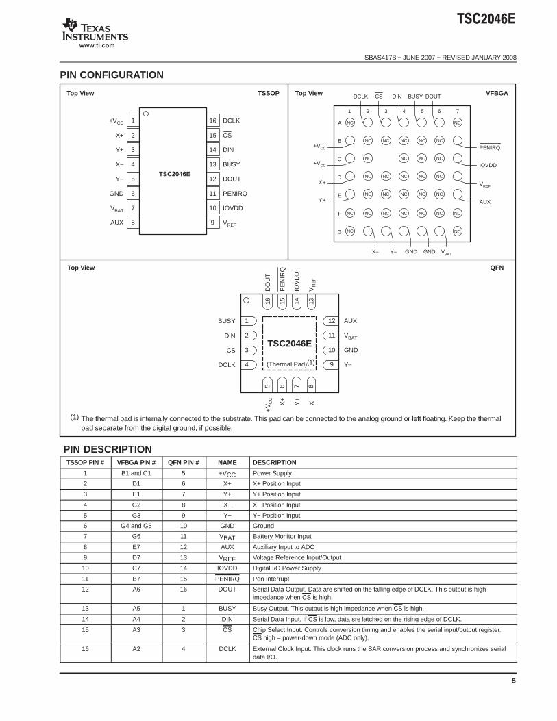
PIN CONFIGURATION
Top View
1
2
3
4
5
6
7
8
+VCC
X+
Y+
X−
Y−
GND
VBAT
AUX
DCLK
CS
DIN
BUSY
DOUT
PENIRQ
IOVDD
VREF
16
15
14
13
12
11
10
9
TSC2046E
Top View QFN
TSSOP Top View VFBGA
NC
NCA
B
C
D
E
F
G
21 3 4 5 6 7
DCLK
+VCC
+VCC
X+
Y+
PENIRQ
IOVDD
VREF
AUX
CS DIN BUSY DOUT
X− Y− GND GND VBAT
NC
NC
NC
NC
NC
NC
NC
NC
NC
NC
NC
NC
NC
NC
NC
NC
NC
NC
NC
NC NC
NC
NC
NC
NC
NCNC
NC
BUSY
DIN
CS
DCLK
AUX
VBAT
GND
Y−
1
2
3
4
12
11
10
9
TSC2046E
DO
UT
PE
NIR
Q
IOV
DD
VR
EF
16 15 14 13
+V
CC
X+
Y+
X−
5 6 7 8
(1) The thermal pad is internally connected to the substrate. This pad can be connected to the analog ground or left floating. Keep the thermalpad separate from the digital ground, if possible.
THEORY OF OPERATIONThe TSC2046E is a classic successive approximationregister (SAR) analog-to-digital converter (ADC). Thearchitecture is based on capacitive redistribution, whichinherently includes a sample-and-hold function. Theconverter is fabricated on a 0.6µm CMOS process.
The basic operation of the TSC2046E is shown inFigure 1. The device features an internal 2.5V referenceand uses an external clock. Operation is maintained froma single supply of 2.7V to 5.25V. The internal reference canbe overdriven with an external, low-impedance sourcebetween 1V and +VCC. The value of the reference voltagedirectly sets the input range of the converter.
The analog input (X-, Y-, and Z-Position coordinates,auxiliary input, battery voltage, and chip temperature)to the converter is provided via a multiplexer. A uniqueconfiguration of low on-resistance touch panel driverswitches allows an unselected ADC input channel toprovide power and the accompanying pin to provideground for an external device, such as a touch screen.By maintaining a differential input to the converter anda differential reference architecture, it is possible tonegate the error from each touch panel driver switchon-resistance (if this is a source of error for theparticular measurement).
+VCC
+VCC
X+
Y+
X−
Y−
VBAT
AUX
B1
C1
D1
E1
G2
G3
G6
E7
G4 G5
A2
A3
A4
A5
A6
B7
C7
D7
DCLK
CS
DIN
BUSY
DOUT
PENIRQ
IOVDD
VREF
Serial/Conversion Clock
Chip Select
Serial Data In
Converter Status
Serial Data Out
+1µF
to10µF
(Optional)
+2.7V to +5VTSC2046E
Auxiliary Input
To Battery
VoltageRegulator
TouchScreen
0.1µF
Pen Interrupt
GND GND
NOTE: VFBGA package and pin names shown.
Figure 1. Basic Operation of the TSC2046E
"#$%&'
SBAS417B − JUNE 2007 − REVISED JANUARY 2008
www.ti.com
10
ANALOG INPUT
Figure 2 shows a block diagram of the input multiplexer onthe TSC2046E, the differential input of the ADC, and thedifferential reference of the converter. Table 1 and Table 2show the relationship between the A2, A1, A0, andSER/DFR control bits and the configuration of theTSC2046E. The control bits are provided serially via the DINpin—see the Digital Interface section of this data sheet formore details.
When the converter enters the hold mode, the voltagedifference between the +IN and –IN inputs (shown inFigure 2) is captured on the internal capacitor array. Theinput current into the analog inputs depends on theconversion rate of the device. During the sample period, thesource must charge the internal sampling capacitor (typically25pF). After the capacitor is fully charged, there is no furtherinput current. The rate of charge transfer from the analogsource to the converter is a function of conversion rate.
The TSC2046E has an internal 2.5V voltage reference thatcan be turned on or off with the control bit, PD1 (see Table 5and Figure 3). Typically, the internal reference voltage is onlyused in the single-ended mode for battery monitoring,temperature measurement, and for using the auxiliary input.Optimal touch screen performance is achieved when usingthe differential mode. The internal reference voltage of theTSC2046E must be commanded to be off to maintaincompatibility with the ADS7843. Therefore, after power-up,a write of PD1 = 0 is required to ensure the reference is off(see the Typical Characteristics for power-up time of thereference from power-down).
BufferBandGap
ReferencePower−Down
ToCDAC
Optional
VREF
Figure 3. Simplified Diagram of the InternalReference
REFERENCE INPUT
The voltage difference between +REF and –REF (seeFigure 2) sets the analog input range. The TSC2046Eoperates with a reference in the range of 1V to +VCC. Thereare several critical items concerning the reference inputand its wide voltage range. As the reference voltage isreduced, the analog voltage weight of each digital outputcode (referred to as LSB size) is also reduced. The LSB(least significant bit) size is equal to the reference voltagedivided by 4096 in 12-bit mode. Any offset or gain errorinherent in the ADC appears to increase, in terms of LSBsize, as the reference voltage is reduced. For example, ifthe offset of a given converter is 2LSBs with a 2.5Vreference, it is typically 5LSBs with a 1V reference. In eachcase, the actual offset of the device is the same, 1.22mV.With a lower reference voltage, more care must be takento provide a clean layout including adequate bypassing, aclean (low-noise, low-ripple) power supply, a low-noisereference (if an external reference is used), and alow-noise input signal.
The voltage into the VREF input directly drives thecapacitor digital-to-analog converter (CDAC) portion of theTSC2046E. Therefore, the input current is very low(typically < 13µA).
There is also a critical item regarding the reference whenmaking measurements while the switch drivers are ON. Forthis discussion, it is useful to consider the basic operation ofthe TSC2046E (see Figure 1). This particular applicationshows the device being used to digitize a resistive touchscreen. A measurement of the current Y-Position of thepointing device is made by connecting the X+ input to theADC, turning on the Y+ and Y– drivers, and digitizing thevoltage on X+ (Figure 4 shows a block diagram). For thismeasurement, the resistance in the X+ lead does not affectthe conversion (it does affect the settling time, but theresistance is usually small enough that this is not a concern).However, because the resistance between Y+ and Y– isfairly low, the on-resistance of the Y drivers does make asmall difference. Under the situation outlined so far, it is notpossible to achieve a 0V input or a full-scale input regardlessof where the pointing device is on the touch screen becausesome voltage is lost across the internal switches. In addition,the internal switch resistance is unlikely to track theresistance of the touch screen, providing an additionalsource of error.
Converter
+IN +REF
Y+
+VCC VREF
X+
Y−
GND
−REF−IN
Figure 4. Simplified Diagram of Single-EndedReference (SER/DFR high, Y switches enabled,
X+ is analog input)
This situation can be remedied as shown in Figure 5. Bysetting the SER/DFR bit low, the +REF and –REF inputsare connected directly to Y+ and Y–, respectively, makingthe analog-to-digital conversion ratiometric. The result ofthe conversion is always a percentage of the externalresistance, regardless of how it changes in relation to theon-resistance of the internal switches. Note that there is animportant consideration regarding power dissipation whenusing the ratiometric mode of operation (see the PowerDissipation section for more details).
"#$%&'
SBAS417B − JUNE 2007 − REVISED JANUARY 2008
www.ti.com
12
Converter
+IN +REF
Y+
+VCC
X+
Y−
GND
−REF−IN
Figure 5. Simplified Diagram of DifferentialReference (SER/DFR low, Y switches enabled,
X+ is analog input)
As a final note about the differential reference mode, itmust be used with +VCC as the source of the +REF voltageand cannot be used with VREF. It is possible to use ahigh-precision reference on VREF and single-endedreference mode for measurements that do not need to beratiometric. In some cases, it is possible to power theconverter directly from a precision reference. Mostreferences can provide enough power for the TSC2046E,but might not be able to supply enough current for theexternal load (such as a resistive touch screen).
TOUCH SCREEN SETTLING
In some applications, external capacitors may be requiredacross the touch screen for filtering noise picked up by thetouch screen (for example, noise generated by the LCDpanel or backlight circuitry). These capacitors provide alow-pass filter to reduce the noise, but cause a settling timerequirement when the panel is touched that typicallyshows up as a gain error. There are several methods forminimizing or eliminating this issue. The problem is thatthe input and/or reference has not settled to the finalsteady-state value prior to the ADC sampling the input(s)and providing the digital output. Additionally, the referencevoltage may still be changing during the measurementcycle. Option 1 is to stop or slow down the TSC2046EDCLK for the required touch screen settling time. Thisoption allows the input and reference to have stable valuesfor the Acquire period (3 clock cycles of the TSC2046E;see Figure 9). This option works for both the single-endedand the differential modes. Option 2 is to operate theTSC2046E in the differential mode only for the touchscreen measurements and command the TSC2046E toremain on (touch screen drivers ON) and not go intopower-down (PD0 = 1). Several conversions are made,depending on the settling time required and the
TSC2046E data rate. Once the required number ofconversions have been made, the processor commandsthe TSC2046E to go into its power-down state on the lastmeasurement. This process is required for X-Position,Y-Position, and Z-Position measurements. Option 3 is tooperate in the 15 Clock-per-Conversion mode, whichoverlaps the analog-to-digital conversions and maintainsthe touch screen drivers on until commanded to stop by theprocessor (see Figure 13).
TEMPERATURE MEASUREMENT
In some applications, such as battery recharging, ameasurement of ambient temperature is required. Thetemperature measurement technique used in theTSC2046E relies on the characteristics of asemiconductor junction operating at a fixed current level.The forward diode voltage (VBE) has a well-definedcharacteristic versus temperature. The ambienttemperature can be predicted in applications by knowingthe +25°C value of the VBE voltage and then monitoring thedelta of that voltage as the temperature changes. TheTSC2046E offers two modes of operation. The first moderequires calibration at a known temperature, but onlyrequires a single reading to predict the ambienttemperature. A diode is used (turned on) during thismeasurement cycle. The voltage across the diode isconnected through the MUX for digitizing the forward biasvoltage by the ADC with an address of A2 = 0, A1 = 0, andA0 = 0 (see Table 1 and Figure 6 for details). This voltageis typically 600mV at +25°C with a 20µA current throughthe diode. The absolute value of this diode voltage canvary by a few millivolts. However, the temperaturecoefficient (TC) of this voltage is very consistent at–2.1mV/°C. During the final test of the end product, thediode voltage would be stored at a known roomtemperature, in memory, for calibration purposes by theuser. The result is an equivalent temperaturemeasurement resolution of 0.3°C/LSB (in 12-bit mode).
The second mode of operation does not require a testtemperature calibration, but uses a two-measurementmethod to eliminate the need for absolute temperaturecalibration and for achieving 2°C accuracy. This moderequires a second conversion with an address of A2 = 1,A1 = 1, and A0 = 1, with a 91 times larger current. The voltagedifference between the first and second conversion using 91times the bias current is represented by Equation (1):
V
kTq In(N)
where:
N is the current ratio = 91.
k = Boltzmann’s constant = 1.3807 × 10⁻²³ J/K(joules/kelvins).
q = the electron charge = 1.6022 × 10⁻¹⁹ C (coulombs).
T = the temperature in kelvins (K).
This method can provide improved absolute temperaturemeasurement, but at a lower resolution of 1.6°C/LSB. Theresulting equation that solves for T is:
T
q Vk In(N)
where:
∆V = VBE(TEMP1) – VBE(TEMP0) (in mV)
∴ T = 2.573 ⋅ ∆V (in K)
or T = 2.573 ⋅ ∆V – 273 (in °C)
NOTE: The bias current for each diode temperaturemeasurement is only on for three clock cycles (during theacquisition mode) and, therefore, does not add anynoticeable increase in power, especially if the temperaturemeasurement only occurs occasionally.
BATTERY MEASUREMENT
An added feature of the TSC2046E is the ability to monitorthe battery voltage on the other side of the voltage regulator(dc/dc converter), as shown in Figure 7. The battery voltagecan vary from 0V to 6V, while maintaining the voltage to theTSC2046E at 2.7V, 3.3V, etc. The input voltage (VBAT) isdivided down by four so that a 5.5V battery voltage isrepresented as 1.375V to the ADC. This design simplifies themultiplexer and control logic. In order to minimize the powerconsumption, the divider is only on during the samplingperiod when A2 = 0, A1 = 1, and A0 = 0 (see Table 1 for therelationship between the control bits and configuration of theTSC2046E).
Measuring touch pressure can also be done with theTSC2046E. To determine pen or finger touch, the pressureof the touch needs to be determined. Generally, it is notnecessary to have very high performance for this test;therefore, the 8-bit resolution mode is recommended(however, calculations shown here are in the 12-bitresolution mode). There are several different ways ofperforming this measurement. The TSC2046E supportstwo methods. The first method requires knowing theX-plate resistance, measurement of the X-Position, andtwo additional cross panel measurements (Z1 and Z2) ofthe touch screen, as shown in Figure 8. Using Equation (3)calculates the touch resistance:
RTOUCH RX−Plate X−Position
4096
Z2
Z11
The second method requires knowing both the X-plateand Y-plate resistance, measurement of X-Position andY-Position, and Z1. Using Equation (4) also calculatesthe touch resistance:
RTOUCH
RX−Plate X−Position4096
4096
Z11
RY−Plate1Y−Position
4096
DIGITAL INTERFACE
See Figure 9 for the typical operation of the TSC2046Edigital interface. This diagram assumes that the source ofthe digital signals is a microcontroller or digital signalprocessor with a basic serial interface. Eachcommunication between the processor and the converter,such as SPI, SSI, or Microwire synchronous serialinterface, consists of eight clock cycles. One completeconversion can be accomplished with three serialcommunications for a total of 24 clock cycles on the DCLKinput.
The first eight clock cycles are used to provide the controlbyte via the DIN pin. When the converter has enoughinformation about the following conversion to set the inputmultiplexer and reference inputs appropriately, theconverter enters the acquisition (sample) mode and, ifneeded, the touch panel drivers are turned on. After threemore clock cycles, the control byte is complete and theconverter enters the conversion mode. At this point, theinput sample-and-hold goes into the hold mode and thetouch panel drivers turn off (in single-ended mode). Thenext 12 clock cycles accomplish the actual analog-to-digital conversion. If the conversion is ratiometric(SER/DFR = 0), the drivers are on during the conversionand a 13th clock cycle is needed for the last bit of theconversion result. Three more clock cycles are needed tocomplete the last byte (DOUT will be low), which areignored by the converter.
X−Position
MeasureX−Position
Touch
X+ Y+
X− Y−
MeasureZ1−Position
Z1−Position
Touch
X+ Y+
Y−X− MeasureZ2−Position
Z2−Position
Touch
X+ Y+
Y−X−
Figure 8. Pressure Measurement Block Diagrams
(3)
(4)
"#$%&'
SBAS417B − JUNE 2007 − REVISED JANUARY 2008
www.ti.com
15
Control Byte
The control byte (on DIN), as shown in Table 3, providesthe start conversion, addressing, ADC resolution,configuration, and power-down of the TSC2046E.Figure 9, Table 3 and Table 4 give detailed informationregarding the order and description of these control bitswithin the control byte.
Initiate START —The first bit, the S bit, must always behigh and initiates the start of the control byte. TheTSC2046E ignores inputs on the DIN pin until the start bitis detected.
Addressing —The next three bits (A2, A1, and A0) selectthe active input channel(s) of the input multiplexer (seeTable 1, Table 2, and Figure 2), touch screen drivers, andthe reference inputs.
MODE—The mode bit sets the resolution of the ADC. Withthis bit low, the next conversion has 12-bit resolution,whereas with this bit high, the next conversion has 8-bitresolution.
SER/DFR—The SER/DFR bit controls the referencemode, either single-ended (high) or differential (low). Thedifferential mode is also referred to as the ratiometricconversion mode and is preferred for X-Position,Y-Position, and Pressure-Touch measurements foroptimum performance. The reference is derived from thevoltage at the switch drivers, which is almost the same asthe voltage to the touch screen. In this case, a referencevoltage is not needed as the reference voltage to the ADCis the voltage across the touch screen. In the single-ended
mode, the converter reference voltage is always thedifference between the VREF and GND pins (see Table 1and Table 2, and Figure 2 through Figure 5, for furtherinformation).
BIT 7(MSB) BIT 6 BIT 5 BIT 4 BIT 3 BIT 2 BIT 1
BIT 0(LSB)
S A2 A1 A0 MODE SER/DFR PD1 PD0
Table 3. Order of the Control Bits in the ControlByte
BIT NAME DESCRIPTION
7 S Start bit. Control byte starts with first high bit on DIN.A new control byte can start every 15th clock cyclein 12-bit conversion mode or every 11th clock cyclein 8-bit conversion mode (see Figure 13).
6-4 A2-A0 Channel Select bits. Along with the SER/DFR bit,these bits control the setting of the multiplexer input,touch driver switches, and reference inputs (seeTable 1 and Figure 13).
3 MODE 12-Bit/8-Bit Conversion Select bit. This bit controlsthe number of bits for the next conversion: 12-bits(low) or 8-bits (high).
2 SER/DFR Single-Ended/Differential Reference Select bit. Alongwith bits A2-A0, this bit controls the setting of themultiplexer input, touch driver switches, andreference inputs (see Table 1 and Table 2).
Table 4. Descriptions of the Control Bits withinthe Control Byte
p
tACQ
AcquireIdle Conversion Idle
1DCLK
CS
8 1
11DOUT
BUSY
Drivers 1 and 2(1)
(SER/DFR High)
Drivers 1 and 2(1, 2)
(SER/DFR Low)
(MSB)
(START)
(LSB)
A2S
On
On
Off Off
Off Off
DIN A1 A0 MODESER/DFR PD1 PD0
10 9 8 7 6 5 4 3 2 1 0 Zero Filled...
8 1 8
(1) For Y−Position, Driver 1 is on X+ is selected, and Driver 2 is off. For X−Position, Driver 1 is off, Y+ is selected, and Driver 2 is on. Y− will turn on
when power−down mode is entered and PD0 = 0.
(2) Drivers will remain on if PD0 = 1 (no power down) until selected input channel, reference mode, or ower−down mode is changed, or CS is high.
NOTES:
Figure 9. Conversion Timing, 24 Clocks-per-Conversion, 8-Bit Bus Interface. No DCLK delay required with dedicated serial port
"#$%&'
SBAS417B − JUNE 2007 − REVISED JANUARY 2008
www.ti.com
16
If X-Position, Y-Position, and Pressure-Touch aremeasured in the single-ended mode, an external referencevoltage is needed. The TSC2046E must also be poweredfrom the external reference. Caution should be observedwhen using the single-ended mode such that the inputvoltage to the ADC does not exceed the internal referencevoltage, especially if the supply voltage is greater than2.7V.
NOTE: The differential mode can only be used forX-Position, Y-Position, and Pressure-Touchmeasurements. All other measurements require thesingle-ended mode.
PD0 and PD1—Table 5 describes the power-down andthe internal reference voltage configurations. The internalreference voltage can be turned on or off independently ofthe ADC. This feature can allow extra time for the internalreference voltage to settle to the final value prior to makinga conversion. Make sure to also allow this extra wake-uptime if the internal reference is powered down. The ADCrequires no wake-up time and can be instantaneouslyused. Also note that the status of the internal referencepower-down is latched into the part (internally) with BUSYgoing high. In order to turn the reference off, an additionalwrite to the TSC2046E is required after the channel hasbeen converted.
PD1 PD0 PENIRQ DESCRIPTION
0 0 Enabled Power-Down Between Conversions. Wheneach conversion is finished, the converterenters a low-power mode. At the start of thenext conversion, the device instantly powers upto full power. There is no need for additionaldelays to ensure full operation, and the very firstconversion is valid. The Y− switch is on when inpower-down.
0 1 Disabled Reference is off and ADC is on.
1 0 Enabled Reference is on and ADC is off.
1 1 Disabled Device is always powered. Reference is on andADC is on.
Table 5. Power-Down and Internal ReferenceSelection
PENIRQ OUTPUTThe pen-interrupt output function is shown in Figure 10.While in power-down mode with PD0 = 0, the Y-driver is onand connects the Y-plane of the touch screen to GND. ThePENIRQ output is connected to the X+ input through twotransmission gates. When the screen is touched, the X+input is pulled to ground through the touch screen.
In most of the TSC2046E models, the internal pullup resistorvalue is nominally 50kΩ, but this value may vary between36kΩ and 67kΩ given process and temperature variations.In order to assure a logic low of 0.35 (+VCC) is presentedto the PENIRQ circuitry, the total resistance between the X+and Y− terminals must be less than 21kΩ.
PENIRQ
+VCC
50kΩor
90kΩ
On
Y+ or X+ drivers on,or TEMP0, TEMP1
measurements activated.
Y+
X+
Y−
TEMP0 TEMP1
TEMPDIODE
High exceptwhen TEMP0,
TEMP1 activated.
+VCC LevelShifter
IOVDD
Figure 10. PENIRQ Functional Block Diagram
The −90 version of the TSC2046E uses a nominal 90kΩpullup resistor that allows the total resistance between theX+ and Y− terminals to be as high as 30kΩ. Note that thehigher pullup resistance causes a slower response time ofthe PENIRQ to a screen touch, so user software shouldtake this into account.
The PENIRQ output goes low due to the current path throughthe touch screen to ground, initiating an interrupt to theprocessor. During the measurement cycle for X-, Y-, andZ-Position, the X+ input is disconnected from the PENIRQinternal pull-up resistor. This disconnection is done toeliminate any leakage current from the internal pull-upresistor through the touch screen, thus causing no errors.
Furthermore, the PENIRQ output is disabled and low duringthe measurement cycle for X-, Y-, and Z-Position. ThePENIRQ output is disabled and high during themeasurement cycle for battery monitor, auxiliary input, andchip temperature. If the last control byte written to theTSC2046E contains PD0 = 1, the pen-interrupt outputfunction is disabled and is not able to detect when the screenis touched. In order to re-enable the pen-interrupt outputfunction under these circumstances, a control byte needs tobe written to the TSC2046E with PD0 = 0. If the last controlbyte written to the TSC2046E contains PD0 = 0, thepen-interrupt output function is enabled at the end of theconversion. The end of the conversion occurs on the fallingedge of DCLK after bit 1 of the converted data is clocked outof the TSC2046E.
It is recommended that the processor mask the interrupt thatPENIRQ is associated with whenever the processor sendsa control byte to the TSC2046E. This masking prevents falsetriggering of interrupts when the PENIRQ output is disabledin the cases discussed in this section.
"#$%&'
SBAS417B − JUNE 2007 − REVISED JANUARY 2008
www.ti.com
17
16 Clocks-per-Conversion
The control bits for conversion n + 1 can be overlappedwith conversion n to allow for a conversion every 16 clockcycles, as shown in Figure 11. This figure also showspossible serial communication occurring with other serialperipherals between each byte transfer from the processorto the converter. (16 clocks cycles are possible, providedthat each conversion completes within 1.6ms of starting.Otherwise, the signal that is captured on the inputsample-and-hold may droop enough to affect theconversion result.) Note that the TSC2046E is fullypowered while other serial communications are takingplace during a conversion.
Digital Timing
Figure 9, Figure 12, and Table 6 provide detailed timing forthe digital interface of the TSC2046E.
15 Clocks-per-Conversion
Figure 13 provides the fastest way to clock theTSC2046E. This method does not work with the serialinterface of most microcontrollers and digital signalprocessors, as they are generally not capable of providing15 clock cycles per serial transfer. However, this methodcan be used with field-programmable gate arrays (FPGAs)or application- specific integrated circuits (ASICs). Notethat this effectively increases the maximum conversionrate of the converter beyond the values given in thespecification tables, which assume 16 clock cycles perconversion.
1
DCLK
CS
8 1
11DOUT
BUSY
SDIN
Control Bits
S
Control Bits
10 9 8 7 6 5 4 3 2 1 0 11 10 9
8 1 18
Figure 11. Conversion Timing, 16 Clocks-per-Conversion, 8-Bit Bus Interface. No DCLK delay required with dedicated serial port
PD0
tBDV
tDH
tCH
tCL
tDS
tCSS
tDV
tBD tBD
tTR
tBTR
tDO tCSH
DCLK
CS
11DOUT
BUSY
DIN
10
Figure 12. Detailed Timing Diagram
"#$%&'
SBAS417B − JUNE 2007 − REVISED JANUARY 2008
www.ti.com
18
+VCC 2.7V, +VCC IOVDD 1.5V, CLOAD = 50pF
SYMBOL DESCRIPTION MIN TYP MAX UNITS
tACQ Acquisition Time 1.5 µs
tDS DIN Valid Prior to DCLK Rising 100 ns
tDH DIN Hold After DCLK High 50 ns
tDO DCLK Falling to DOUT Valid 200 ns
tDV CS Falling to DOUT Enabled 200 ns
tTR CS Rising to DOUT Disabled 200 ns
tCSS CS Falling to First DCLK Rising 100 ns
tCSH CS Rising to DCLK Ignored 10 ns
tCH DCLK High 200 ns
tCL DCLK Low 200 ns
tBD DCLK Falling to BUSY Rising/Falling 200 ns
tBDV CS Falling to BUSY Enabled 200 ns
tBTR CS Rising to BUSY Disabled 200 ns
Table 6. Timing Specifications, T A = −40C to +85C
1
DCLK
CS
11DOUT
BUSY
A2SDIN A1 A0 M O D ESER/
DFR PD1 PD0
10 9 8 7 6 5 4 3 2 1 0 11 10 9 8 7
A1 A0
15 1 15
Power−Down
1
A2S A1 A0 M O D E PD1 PD0 A2SSER/
DFR
Figure 13. Maximum Conversion Rate, 15 Clocks-per-Conversion
Data Format
The TSC2046E output data is in Straight Binary format, asshown in Figure 14. This figure shows the ideal outputcode for the given input voltage and does not include theeffects of offset, gain, or noise.
8-Bit Conversion
The TSC2046E provides an 8-bit conversion mode thatcan be used when faster throughput is needed and thedigital result is not as critical. By switching to the 8-bitmode, a conversion is complete four clock cycles earlier.Not only does this shorten each conversion by four bits(25% faster throughput), but each conversion can actuallyoccur at a faster clock rate. This faster rate occurs becausethe internal settling time of the TSC2046E is not ascritical—settling to better than 8 bits is all that is needed.The clock rate can be as much as 50% faster. The fasterclock rate and fewer clock cycles combine to provide a 2xincrease in conversion rate.
Out
putC
ode
0V
FS = Full−Scale Voltage = VREF(1)
1LSB = VREF(1)/4096
FS − 1LSB
11...111
11...110
11...101
00...010
00...001
00...000
1LSB
NOTES:
Input Voltage(2) (V)
(1) Reference voltage at converter: +REF − (−REF); see Figure 2.(2) Input voltage at converter, after multiplexer: +IN − (−IN); see
Figure 2.
Figure 14. Ideal Input Voltages and Output Codes
"#$%&'
SBAS417B − JUNE 2007 − REVISED JANUARY 2008
www.ti.com
19
POWER DISSIPATION
There are two major power modes for the TSC2046E:full-power (PD0 = 1) and auto power-down (PD0 = 0).When operating at full speed and 16clocks-per-conversion (see Figure 11), the TSC2046Espends most of the time acquiring or converting. There islittle time for auto power-down, assuming that this mode isactive. Therefore, the difference between full-power modeand auto power-down is negligible. If the conversion rateis decreased by slowing the frequency of the DCLK input,the two modes remain approximately equal. However, ifthe DCLK frequency is kept at the maximum rate during aconversion but conversions are done less often, thedifference between the two modes is dramatic.
Figure 15 shows the difference between reducing theDCLK frequency (scaling DCLK to match the conversionrate) or maintaining DCLK at the highest frequency andreducing the number of conversions per second. In thelatter case, the converter spends an increasingpercentage of time in power-down mode (assuming theauto power-down mode is active).
1k 1M10k 100k
fSAMPLE (Hz)
Sup
ply
Cu
rren
t(µ
A)
1000
100
10
1
fCLK = 2MHzSupply Current from
+VC C and IOVDD
TA = 25¡C+VCC = 2.7V
IOVDD = 1.8V
fCLK = 16 ⋅ fSAMPLE
Figure 15. Supply Current versus Directly Scalingthe Frequency of DCLK with Sample Rate orMaintaining DCLK at the Maximum Possible
Frequency
Another important consideration for power dissipation isthe reference mode of the converter. In the single-endedreference mode, the touch panel drivers are ON only whenthe analog input voltage is being acquired (see Figure 9and Table 1). The external device (for example, a resistivetouch screen), therefore, is only powered during theacquisition period. In the differential reference mode, theexternal device must be powered throughout theacquisition and conversion periods (see Figure 9). If theconversion rate is high, it could substantially increasepower dissipation.
CS also puts the TSC2046E into power-down mode.When CS goes high, the TSC2046E immediately goes intopower-down mode and does not complete the currentconversion. The internal reference, however, does not turnoff with CS going high. To turn the reference off, anadditional write is required before CS goes high (PD1 = 0).
When the TSC2046E first powers up, the device drawsabout 20µA of current until a control byte is written to it withPD0 = 0 to put it into power-down mode. This current drawcan be avoided if the TSC2046E is powered up with CS =0 and DCLK = IOVDD.
"#$%&'
SBAS417B − JUNE 2007 − REVISED JANUARY 2008
www.ti.com
20
LAYOUTThe following layout suggestions provide the mostoptimum performance from the TSC2046E. Many portableapplications, however, have conflicting requirementsconcerning power, cost, size, and weight. In general, mostportable devices have fairly clean power and groundsbecause most of the internal components are very lowpower. This situation means less bypassing for theconverter power and less concern regarding grounding.Still, each situation is unique and the followingsuggestions should be reviewed carefully.
For optimum performance, care should be taken with thephysical layout of the TSC2046E circuitry. The basic SARarchitecture is sensitive to glitches or sudden changes onthe power supply, reference, ground connections, anddigital inputs that occur just prior to latching the output ofthe analog comparator. Therefore, during any singleconversion for an n-bit SAR converter, there are n windowsin which large external transient voltages can easily affectthe conversion result. Such glitches can originate fromswitching power supplies, nearby digital logic, andhigh-power devices. The degree of error in the digitaloutput depends on the reference voltage, layout, and theexact timing of the external event. The error can change ifthe external event changes in time with respect to theDCLK input.
Because of the SAR architecture sensitvity, power to theTSC2046E should be clean and well bypassed. A 0.1µFceramic bypass capacitor should be placed as close to thedevice as possible. A 1µF to 10µF capacitor may also beneeded if the impedance of the connection between +VCCor IOVDD and the power supplies is high. Low-leakagecapacitors should be used to minimize power dissipationthrough the bypass capacitors when the TSC2046E is inpower-down mode.
A bypass capacitor is generally not needed on the VREFpin because the internal reference is buffered by aninternal op amp. If an external reference voltage originatesfrom an op amp, make sure that it can drive any bypasscapacitor that is used without oscillation.
The TSC2046E architecture offers no inherent rejection ofnoise or voltage variation in regards to using an externalreference input. This is of particular concern when thereference input is tied to the power supply. Any noise andripple from the supply appears directly in the digital results.Whereas high-frequency noise can be filtered out, voltagevariation bacause of line frequency (50Hz or 60Hz) can bedifficult to remove.
The GND pin must be connected to a clean ground point.In many cases, this is the analog ground. Avoidconnections which are too near the grounding point of amicrocontroller or digital signal processor. If needed, runa ground trace directly from the converter to thepower-supply entry or battery connection point. The ideallayout includes an analog ground plane dedicated to theconverter and associated analog circuitry.
In the specific case of use with a resistive touch screen,care should be taken with the connection between theconverter and the touch screen. Although resistive touchscreens have fairly low resistance, the interconnectionshould be as short and robust as possible. Longerconnections are a source of error, much like theon-resistance of the internal switches. Likewise, looseconnections can be a source of error when the contactresistance changes with flexing or vibrations.
As indicated previously, noise can be a major source oferror in touch screen applications (such as in applicationsthat require a backlit LCD panel). This EMI noise can becoupled through the LCD panel to the touch screen andcause flickering of the converted data. Several things canbe done to reduce this error; for instance, using a touchscreen with a bottom-side metal layer connected to groundto shunt the majority of noise to ground. Additionally,filtering capacitors from Y+, Y–, X+, and X− pins to groundcan also help. Caution should be observed under thesecircumstances for settling time of the touch screen,especially operating in the single-ended mode and at highdata rates.
"#$%&'
SBAS417B − JUNE 2007 − REVISED JANUARY 2008
www.ti.com
21
Revision History
DATE REV PAGE SECTION DESCRIPTION
1/08 B3, 4 Electrical Characteristics Fixed typos in conditions header and in Note (6).
1/08 B13 Temperature Measurement Fixed typos in Equations (1) and (2).
8/07 A 5 Pin Configuration Added note to QFN package.
NOTE: Page numbers for previous revisions may differ from page numbers in the current version.
PACKAGE OPTION ADDENDUM
www.ti.com 15-Apr-2017
Addendum-Page 1
PACKAGING INFORMATION
Orderable Device Status(1)
Package Type PackageDrawing
Pins PackageQty
Eco Plan(2)
Lead/Ball Finish(6)
MSL Peak Temp(3)
Op Temp (°C) Device Marking(4/5)
Samples
TSC2046EIPW ACTIVE TSSOP PW 16 90 Green (RoHS& no Sb/Br)
CU NIPDAU Level-2-260C-1 YEAR -40 to 85 TSC2046EI
TSC2046EIPWG4 ACTIVE TSSOP PW 16 90 Green (RoHS& no Sb/Br)
CU NIPDAU Level-2-260C-1 YEAR -40 to 85 TSC2046EI
TSC2046EIPWR ACTIVE TSSOP PW 16 2000 Green (RoHS& no Sb/Br)
CU NIPDAU Level-2-260C-1 YEAR -40 to 85 TSC2046EI
TSC2046EIPWRG4 ACTIVE TSSOP PW 16 2000 Green (RoHS& no Sb/Br)
CU NIPDAU Level-2-260C-1 YEAR -40 to 85 TSC2046EI
TSC2046EIRGVR ACTIVE VQFN RGV 16 2500 Green (RoHS& no Sb/Br)
CU NIPDAU Level-2-260C-1 YEAR -40 to 85 TSC2046E
TSC2046EIRGVT ACTIVE VQFN RGV 16 250 Green (RoHS& no Sb/Br)
CU NIPDAU Level-2-260C-1 YEAR -40 to 85 TSC2046E
TSC2046EIZQCR ACTIVE BGAMICROSTAR
JUNIOR
ZQC 48 2500 Pb-Free(RoHS)
SNAGCU Level-3-260C-168 HR -40 to 85 BC2046E
TSC2046EIZQCT ACTIVE BGAMICROSTAR
JUNIOR
ZQC 48 250 Pb-Free(RoHS)
SNAGCU Level-3-260C-168 HR -40 to 85 BC2046E
(1) The marketing status values are defined as follows:ACTIVE: Product device recommended for new designs.LIFEBUY: TI has announced that the device will be discontinued, and a lifetime-buy period is in effect.NRND: Not recommended for new designs. Device is in production to support existing customers, but TI does not recommend using this part in a new design.PREVIEW: Device has been announced but is not in production. Samples may or may not be available.OBSOLETE: TI has discontinued the production of the device.
(2) Eco Plan - The planned eco-friendly classification: Pb-Free (RoHS), Pb-Free (RoHS Exempt), or Green (RoHS & no Sb/Br) - please check http://www.ti.com/productcontent for the latest availabilityinformation and additional product content details.TBD: The Pb-Free/Green conversion plan has not been defined.Pb-Free (RoHS): TI's terms "Lead-Free" or "Pb-Free" mean semiconductor products that are compatible with the current RoHS requirements for all 6 substances, including the requirement thatlead not exceed 0.1% by weight in homogeneous materials. Where designed to be soldered at high temperatures, TI Pb-Free products are suitable for use in specified lead-free processes.Pb-Free (RoHS Exempt): This component has a RoHS exemption for either 1) lead-based flip-chip solder bumps used between the die and package, or 2) lead-based die adhesive used betweenthe die and leadframe. The component is otherwise considered Pb-Free (RoHS compatible) as defined above.Green (RoHS & no Sb/Br): TI defines "Green" to mean Pb-Free (RoHS compatible), and free of Bromine (Br) and Antimony (Sb) based flame retardants (Br or Sb do not exceed 0.1% by weightin homogeneous material)
(3) MSL, Peak Temp. - The Moisture Sensitivity Level rating according to the JEDEC industry standard classifications, and peak solder temperature.
(4) There may be additional marking, which relates to the logo, the lot trace code information, or the environmental category on the device.
(5) Multiple Device Markings will be inside parentheses. Only one Device Marking contained in parentheses and separated by a "~" will appear on a device. If a line is indented then it is a continuationof the previous line and the two combined represent the entire Device Marking for that device.
(6) Lead/Ball Finish - Orderable Devices may have multiple material finish options. Finish options are separated by a vertical ruled line. Lead/Ball Finish values may wrap to two lines if the finishvalue exceeds the maximum column width.
Important Information and Disclaimer:The information provided on this page represents TI's knowledge and belief as of the date that it is provided. TI bases its knowledge and belief on informationprovided by third parties, and makes no representation or warranty as to the accuracy of such information. Efforts are underway to better integrate information from third parties. TI has taken andcontinues to take reasonable steps to provide representative and accurate information but may not have conducted destructive testing or chemical analysis on incoming materials and chemicals.TI and TI suppliers consider certain information to be proprietary, and thus CAS numbers and other limited information may not be available for release.
In no event shall TI's liability arising out of such information exceed the total purchase price of the TI part(s) at issue in this document sold by TI to Customer on an annual basis.
OTHER QUALIFIED VERSIONS OF TSC2046E :
• Automotive: TSC2046E-Q1
NOTE: Qualified Version Definitions:
• Automotive - Q100 devices qualified for high-reliability automotive applications targeting zero defects
Texas Instruments Incorporated (TI) reserves the right to make corrections, enhancements, improvements and other changes to itssemiconductor products and services per JESD46, latest issue, and to discontinue any product or service per JESD48, latest issue. Buyersshould obtain the latest relevant information before placing orders and should verify that such information is current and complete.TI’s published terms of sale for semiconductor products (http://www.ti.com/sc/docs/stdterms.htm) apply to the sale of packaged integratedcircuit products that TI has qualified and released to market. Additional terms may apply to the use or sale of other types of TI products andservices.Reproduction of significant portions of TI information in TI data sheets is permissible only if reproduction is without alteration and isaccompanied by all associated warranties, conditions, limitations, and notices. TI is not responsible or liable for such reproduceddocumentation. Information of third parties may be subject to additional restrictions. Resale of TI products or services with statementsdifferent from or beyond the parameters stated by TI for that product or service voids all express and any implied warranties for theassociated TI product or service and is an unfair and deceptive business practice. TI is not responsible or liable for any such statements.Buyers and others who are developing systems that incorporate TI products (collectively, “Designers”) understand and agree that Designersremain responsible for using their independent analysis, evaluation and judgment in designing their applications and that Designers havefull and exclusive responsibility to assure the safety of Designers' applications and compliance of their applications (and of all TI productsused in or for Designers’ applications) with all applicable regulations, laws and other applicable requirements. Designer represents that, withrespect to their applications, Designer has all the necessary expertise to create and implement safeguards that (1) anticipate dangerousconsequences of failures, (2) monitor failures and their consequences, and (3) lessen the likelihood of failures that might cause harm andtake appropriate actions. Designer agrees that prior to using or distributing any applications that include TI products, Designer willthoroughly test such applications and the functionality of such TI products as used in such applications.TI’s provision of technical, application or other design advice, quality characterization, reliability data or other services or information,including, but not limited to, reference designs and materials relating to evaluation modules, (collectively, “TI Resources”) are intended toassist designers who are developing applications that incorporate TI products; by downloading, accessing or using TI Resources in anyway, Designer (individually or, if Designer is acting on behalf of a company, Designer’s company) agrees to use any particular TI Resourcesolely for this purpose and subject to the terms of this Notice.TI’s provision of TI Resources does not expand or otherwise alter TI’s applicable published warranties or warranty disclaimers for TIproducts, and no additional obligations or liabilities arise from TI providing such TI Resources. TI reserves the right to make corrections,enhancements, improvements and other changes to its TI Resources. TI has not conducted any testing other than that specificallydescribed in the published documentation for a particular TI Resource.Designer is authorized to use, copy and modify any individual TI Resource only in connection with the development of applications thatinclude the TI product(s) identified in such TI Resource. NO OTHER LICENSE, EXPRESS OR IMPLIED, BY ESTOPPEL OR OTHERWISETO ANY OTHER TI INTELLECTUAL PROPERTY RIGHT, AND NO LICENSE TO ANY TECHNOLOGY OR INTELLECTUAL PROPERTYRIGHT OF TI OR ANY THIRD PARTY IS GRANTED HEREIN, including but not limited to any patent right, copyright, mask work right, orother intellectual property right relating to any combination, machine, or process in which TI products or services are used. Informationregarding or referencing third-party products or services does not constitute a license to use such products or services, or a warranty orendorsement thereof. Use of TI Resources may require a license from a third party under the patents or other intellectual property of thethird party, or a license from TI under the patents or other intellectual property of TI.TI RESOURCES ARE PROVIDED “AS IS” AND WITH ALL FAULTS. TI DISCLAIMS ALL OTHER WARRANTIES ORREPRESENTATIONS, EXPRESS OR IMPLIED, REGARDING RESOURCES OR USE THEREOF, INCLUDING BUT NOT LIMITED TOACCURACY OR COMPLETENESS, TITLE, ANY EPIDEMIC FAILURE WARRANTY AND ANY IMPLIED WARRANTIES OFMERCHANTABILITY, FITNESS FOR A PARTICULAR PURPOSE, AND NON-INFRINGEMENT OF ANY THIRD PARTY INTELLECTUALPROPERTY RIGHTS. TI SHALL NOT BE LIABLE FOR AND SHALL NOT DEFEND OR INDEMNIFY DESIGNER AGAINST ANY CLAIM,INCLUDING BUT NOT LIMITED TO ANY INFRINGEMENT CLAIM THAT RELATES TO OR IS BASED ON ANY COMBINATION OFPRODUCTS EVEN IF DESCRIBED IN TI RESOURCES OR OTHERWISE. IN NO EVENT SHALL TI BE LIABLE FOR ANY ACTUAL,DIRECT, SPECIAL, COLLATERAL, INDIRECT, PUNITIVE, INCIDENTAL, CONSEQUENTIAL OR EXEMPLARY DAMAGES INCONNECTION WITH OR ARISING OUT OF TI RESOURCES OR USE THEREOF, AND REGARDLESS OF WHETHER TI HAS BEENADVISED OF THE POSSIBILITY OF SUCH DAMAGES.Unless TI has explicitly designated an individual product as meeting the requirements of a particular industry standard (e.g., ISO/TS 16949and ISO 26262), TI is not responsible for any failure to meet such industry standard requirements.Where TI specifically promotes products as facilitating functional safety or as compliant with industry functional safety standards, suchproducts are intended to help enable customers to design and create their own applications that meet applicable functional safety standardsand requirements. Using products in an application does not by itself establish any safety features in the application. Designers mustensure compliance with safety-related requirements and standards applicable to their applications. Designer may not use any TI products inlife-critical medical equipment unless authorized officers of the parties have executed a special contract specifically governing such use.Life-critical medical equipment is medical equipment where failure of such equipment would cause serious bodily injury or death (e.g., lifesupport, pacemakers, defibrillators, heart pumps, neurostimulators, and implantables). Such equipment includes, without limitation, allmedical devices identified by the U.S. Food and Drug Administration as Class III devices and equivalent classifications outside the U.S.TI may expressly designate certain products as completing a particular qualification (e.g., Q100, Military Grade, or Enhanced Product).Designers agree that it has the necessary expertise to select the product with the appropriate qualification designation for their applicationsand that proper product selection is at Designers’ own risk. Designers are solely responsible for compliance with all legal and regulatoryrequirements in connection with such selection.Designer will fully indemnify TI and its representatives against any damages, costs, losses, and/or liabilities arising out of Designer’s non-compliance with the terms and provisions of this Notice.