LP3952 6-Channel Color LED Driver with Audio SynchronizationCheck for Samples: LP3952
1FEATURES APPLICATIONS2• Constant current and PWM controlled color • Cellular Phones
LED drivers • PDAs, MP3 players• Maximum current 40mA / output in constant
current mode, supports also switch mode DESCRIPTIONcontrol with 50 mA maximum current / output LP3952 is a color LED driver for battery powered
handheld devices. It drives any color LEDs including• Complete audio synchronization for color/RGBRGB LEDs, indicator LEDs and keypad backlightLEDs with amplitude, frequency and speedLEDs. The boost DC-DC converter drives highoptimizationcurrent loads with high efficiency. The stand-alone
• Command based lighting pattern generator for command based RGB controller is feature rich andRGB LEDs easy to configure. Different lighting patterns and
blinking sequences can be programmed to driver• Programmable ON/OFF blinking sequences forregisters. Built-in audio synchronization feature allowsRGB1 outputsuser to synchronize the color LEDs to audio signal.• High efficiency Boost DC-DC converter withLED lighting can be controlled either by audio signal
programmable VOUTand fSW amplitude or frequency. There are many controls• I2C compatible interface available for audio synchronization to get desired
lighting effect, including gain, speed, and different• Possibility for external PWM dimming controlfilter settings. The flexible I2C interface allows easy• Small package – 36-bump DSBGA, 3.0 x 3.0 x control of LP3952. LED outputs can be also
0.65 mm controlled with external PWM signal. Small DSBGApackage together with minimum number of externalcomponents is a best fit for handheld devices.
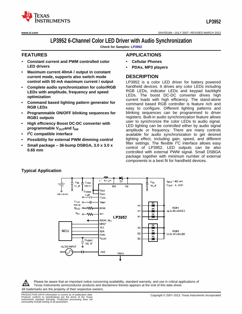
Typical Application
1
Please be aware that an important notice concerning availability, standard warranty, and use in critical applications ofTexas Instruments semiconductor products and disclaimers thereto appears at the end of this data sheet.
2All trademarks are the property of their respective owners.
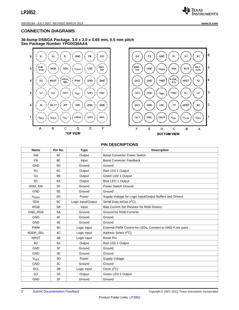
These devices have limited built-in ESD protection. The leads should be shorted together or the device placed in conductive foamduring storage or handling to prevent electrostatic damage to the MOS gates.
Absolute Maximum Ratings (1) (2) (3)
V (SW, FB, R1-2, G1-2, B1-2) (4) (5) -0.3V to +7.2V
VDD1, VDD2, VDDIO, VDDA -0.3V to +6.0V
Voltage on ASE, IRT, IRGB, VREF -0.3V to VDD1+0.3V with 6.0V max
Voltage on Logic Pins -0.3V to VDDIO +0.3V with 6.0V max
V(all other pins): Voltage to GND -0.3V to 6.0V
I (VREF) 10 μA
I(R1, G1, B1, R2, G2, B2) 100 mA
Continuous Power Dissipation (6) Internally Limited
Junction Temperature (TJ-MAX) 150°C
Storage Temperature Range -65°C to +150°C
Maximum Lead Temperature (Soldering) (7) 260°C
ESD Rating (8)
Human Body Model: 2 kV
(1) All voltages are with respect to the potential at the GND pins.(2) Absolute Maximum Ratings indicate limits beyond which damage to the component may occur. Operating Ratings are conditions under
which operation of the device is guaranteed. Operating Ratings do not imply guaranteed performance limits. For guaranteedperformance limits and associated test conditions, see the Electrical Characteristics tables.
(3) If Military/Aerospace specified devices are required, please contact the Texas Instruments Sales Office / Distributors foravailability and specifications.
(4) Battery/Charger voltage should be above 6V no more than 10% of the operational lifetime.(5) Voltage tolerance of LP3952 above 6.0V relies on fact that VDD1 and VDD2 (2.8V) are available (ON) at all conditions. If VDD1 and VDD2
are not available (ON) at all conditions, Texas Instruments does not guarantee any parameters or reliability for this device.(6) Internal thermal shutdown circuitry protects the device from permanent damage. Thermal shutdown engages at TJ=160°C (typ.) and
disengages at TJ=140°C (typ.).(7) For detailed soldering specifications and information, please refer to Application Note AN1412 : DSBGA Wafer Level Chip Scale
Package(8) The Human body model is a 100 pF capacitor discharged through a 1.5 kΩ resistor into each pin.
Operating Ratings (1) (2)
V (SW, FB, R1-2, G1-2, B1-2) 0 to 6.0V
VDD1,2 with external LDO 2.7 to 5.5V
VDD1,2 with internal LDO 3.0 to 5.5V
VDDA 2.7 to 2.9V
(1) Absolute Maximum Ratings indicate limits beyond which damage to the component may occur. Operating Ratings are conditions underwhich operation of the device is guaranteed. Operating Ratings do not imply guaranteed performance limits. For guaranteedperformance limits and associated test conditions, see the Electrical Characteristics tables.
(2) All voltages are with respect to the potential at the GND pins.
Operating Ratings (1) (2) (continued)VDDIO 1.65V to VDD1
Voltage on ASE 0.1V to VDDA –0.1V
Recommended Load Current 0 to 300 mA
Junction Temperature (TJ) Range -30°C to +125°C
Ambient Temperature (TA) Range (3) -30°C to +85°C
(3) In applications where high power dissipation and/or poor package thermal resistance is present, the maximum ambient temperature mayhave to be derated. Maximum ambient temperature (TA-MAX) is dependent on the maximum operating junction temperature (TJ-MAX-OP =125°C), the maximum power dissipation of the device in the application (PD-MAX), and the junction-to ambient thermal resistance of thepart/package in the application (θJA), as given by the following equation: TA-MAX = TJ-MAX-OP – (θJA × PD-MAX).
(1) Junction-to-ambient thermal resistance is highly application and board-layout dependent. In applications where high maximum powerdissipation exists, special care must be paid to thermal dissipation issues in board design.
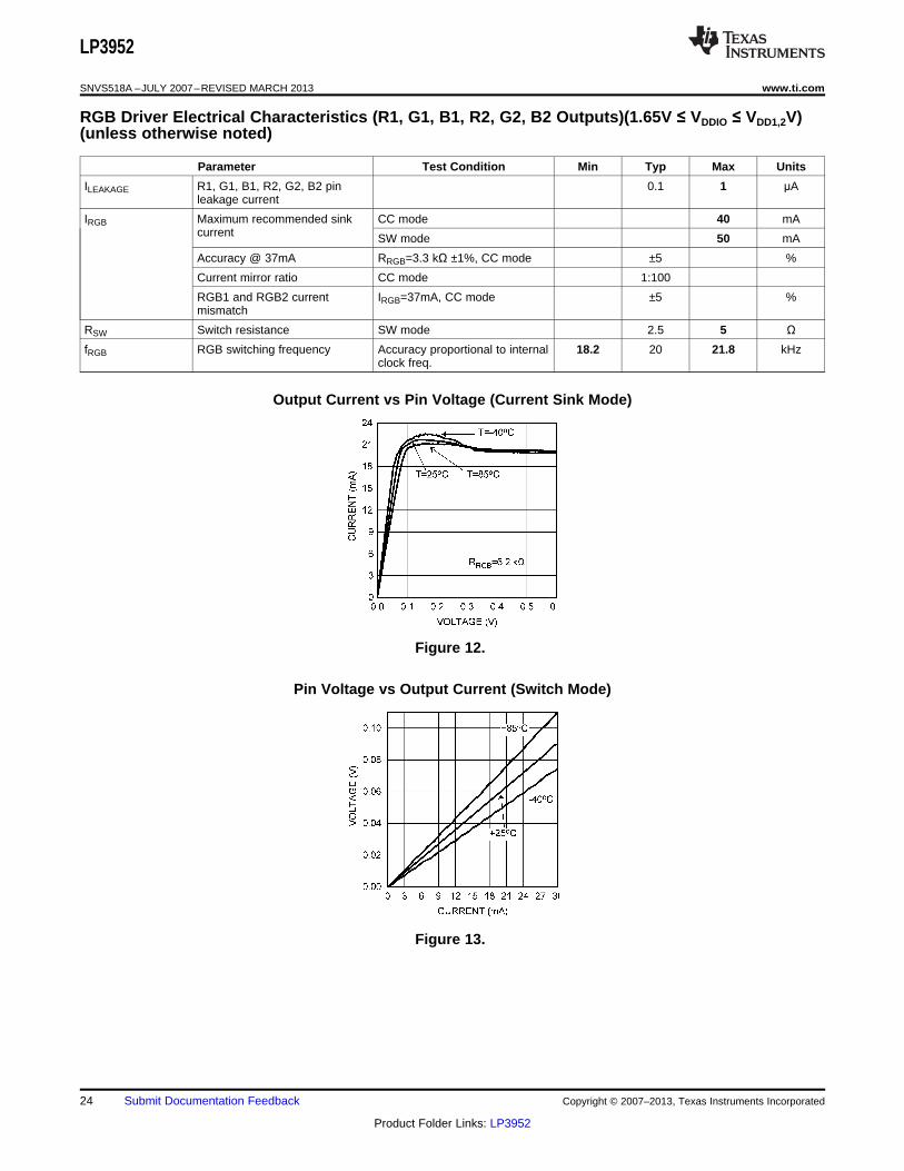
Electrical Characteristics (1) (2)
Limits in standard typeface are for TJ = 25°C. Limits in boldface type apply over the operating ambient temperature range (-30°C < TA < +85°C). Unless otherwise noted, specifications apply to the LP3952 Block Diagram with: VDD1 = VDD2 = 3.6V,VDDIO = 2.8V, CVDD = CVDDIO = 100 nF, COUT = CIN = 10 μF, CVDDA = 1 μF, CREF = 100 nF, L1 = 4.7 μH, RRGB = 5.6 kΩ and RRT
= 82 kΩ (3).
Parameter Test Conditions Min Typ Max Units
IVDD Standby supply current NSTBY (bit) = L, NRST (pin) = H 1 8 μA(VDD1 + VDD2) SCL=H, SDA = H
No-boost supply current NSTBY (bit) = H, 450 μA(VDD1 + VDD2) EN_BOOST(bit) = L
SCL = H, SDA = HAudio sync and LEDs OFF
No-load supply current NSTBY (bit) = H, 1 mA(VDD1 + VDD2) EN_BOOST (bit) = H
SCL = H, SDA = HAudio sync and LEDs OFFAutoload OFF
RGB drivers CC mode at R1, G1, B1 and R2, G2, B2 set to 15 mA 150 μA(VDD1 + VDD2) SW mode 150
VDDA Output voltage of internal (4) 2.72 2.80 2.88 VLDO for analog parts -3 +3 %
(1) All voltages are with respect to the potential at the GND pins.(2) Min and Max limits are guaranteed by design, test, or statistical analysis. Typical numbers are not guaranteed, but do represent the
most likely norm.(3) Low-ESR Surface-Mount Ceramic Capacitors (MLCCs) used in setting electrical characteristics.(4) VDDA output is not recommended for external use.
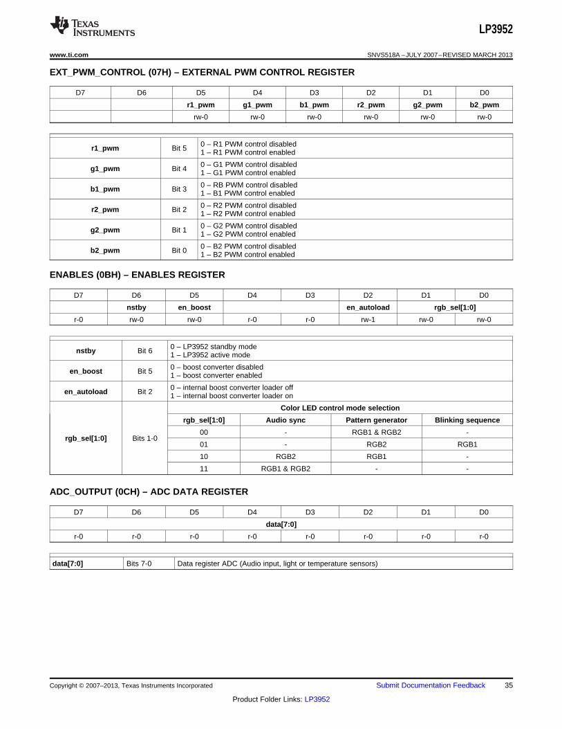
RESET: In the RESET mode all the internal registers are reset to the default values and the chip goes toSTANDBY mode after reset. NSTBY control bit is low after reset by default. Reset is active always ifNRST input pin is low or internal Power On Reset is active. LP3952 can be also reset by writing any datato Reset Register in address 60H. Power On Reset (POR) will activate during the chip startup or when thesupply voltage VDD2 falls below 1.5V. Once VDD2 rises above 1.5V, POR will inactivate and the chip willcontinue to the STANDBY mode.
STANDBY: The STANDBY mode is entered if the register bit NSTBY is LOW. This is the low powerconsumption mode, when all circuit functions are disabled. Registers can be written in this mode and thecontrol bits are effective immediately after power up.
STARTUP: When NSTBY bit is written high, the INTERNAL STARTUP SEQUENCE powers up all the neededinternal blocks (Vref, Bias, Oscillator etc..). To ensure the correct oscillator initialization, a 10 ms delay isgenerated by the internal state-machine. If the chip temperature rises too high, the Thermal Shutdown(TSD) disables the chip operation and STARTUP mode is entered until no thermal shutdown event ispresent.
BOOST STARTUP:Soft start for boost output is generated in the BOOST STARTUP mode. The boost output israised in PFM mode during the 10 ms delay generated by the state-machine. The Boost startup is enteredfrom Internal Startup Sequence if EN_BOOST is HIGH or from Normal mode when EN_BOOST is writtenHIGH. During the 10 ms Boost Startup time all LED outputs are switched off to ensure smooth start-up.
NORMAL: During NORMAL mode the user controls the chip using the Control Registers. The registers can bewritten in any sequence and any number of bits can be altered in a register in one write
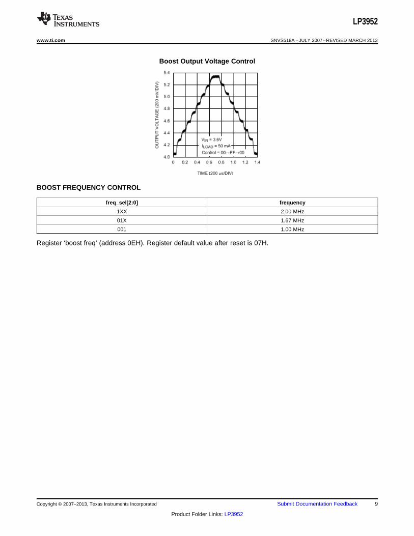
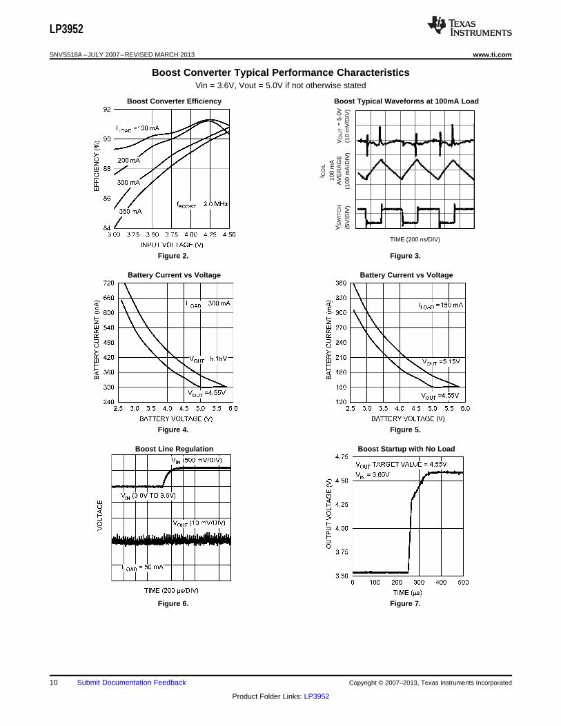
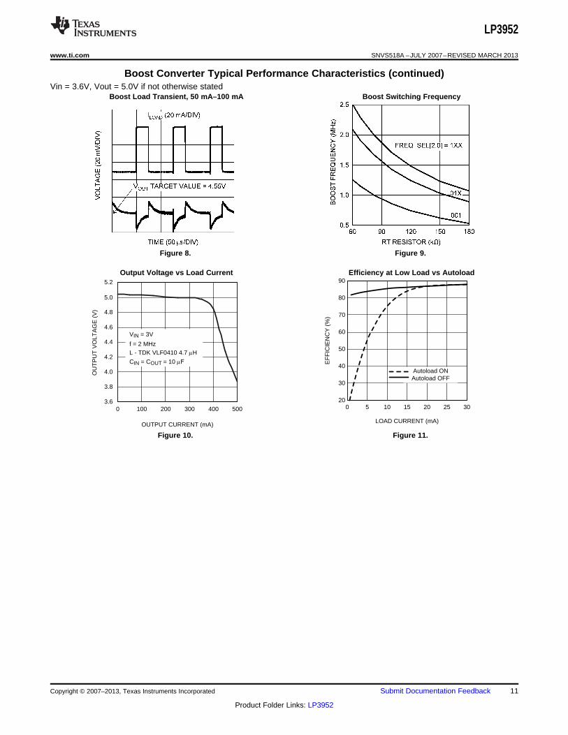
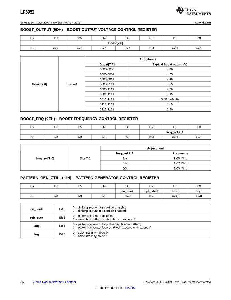
The LP3952 Boost DC/DC Converter generates a 4.0 – 5.3V voltage for the LEDs from single Li-Ion battery(3V…4.5V). The output voltage is controlled with an 8-bit register in 9 steps. The converter is a magneticswitching PWM mode DC/DC converter with a current limit. The converter has three options for switchingfrequency, 1 MHz, 1.67 MHz and 2 MHz (default), when timing resistor RT is 82 kΩ. Timing resistor defines theinternal oscillator frequency and thus directly affects boost frequency and all circuit's internally generated timing(RGB patterns).
The LP3952 Boost Converter uses pulse-skipping elimination to stabilize the noise spectrum. Even with light loador no load a minimum length current pulse is fed to the inductor. An active load is used to remove the excesscharge from the output capacitor at very light loads. At very light load and when input and output voltages arevery close to each other, the pulse skipping is not completely eliminated. Output voltage should be at least 0.5Vhigher than input voltage to avoid pulse skipping. Reducing the switching frequency will also reduce the requiredvoltage difference.
Active load can be disabled with the en_autoload bit. Disabling will increase the efficiency at light loads, but thedownside is that pulse skipping will occur. The Boost Converter should be stopped when there is no load tominimise the current consumption.
The topology of the magnetic boost converter is called CPM control, current programmed mode, where theinductor current is measured and controlled with the feedback. The user can program the output voltage of theboost converter. The output voltage control changes the resistor divider in the feedback loop.
The following figure shows the boost topology with the protection circuitry. Four different protection schemes areimplemented:1. Over voltage protection, limits the maximum output voltage
– Keeps the output below breakdown voltage.– Prevents boost operation if battery voltage is much higher than desired output.
2. Over current protection, limits the maximum inductor current– Voltage over switching NMOS is monitored; too high voltages turn the switch off.
3. Feedback break protection. Prevents uncontrolled operation if FB pin gets disconnected.4. Duty cycle limiting, done with digital control.
tSTARTUP Startup Time Boost startup from STANDBY 10 ms
ISW_MAX SW Pin Current Limit 700 800 900mA
550 950
BOOST STANDBY MODE
User can stop the Boost Converter operation by writing the Enables register bit EN_BOOST low. WhenEN_BOOST is written high, the converter starts for 10 ms in PFM mode and then goes to PWM mode.
BOOST OUTPUT VOLTAGE CONTROL
User can control the boost output voltage by boost output 8-bit register.
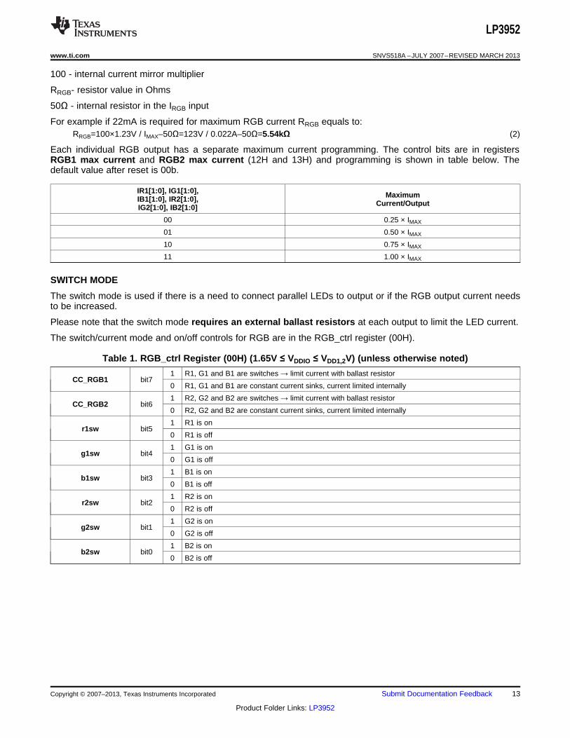
FUNCTIONALITY OF COLOR LED OUTPUTS (R1, G1, B1; R2, G2, B2)
The LP3952 has 2 sets of RGB/color LED outputs. Both sets have 3 outputs and the sets can be controlled in 4different ways:1. Command based pattern generator control (internal PWM)2. Audio synchronization control3. Programmable ON/OFF blinking sequences for RGB14. External PWM control
By using command based pattern generator user can program any kind of color effect patterns. LED intensity,blinking cycles and slopes are independently controlled with 8 16-bit commands. Also real time commands arepossible as well as loops and step by step control. If analog audio is available on system, the user can useaudio synchronization for synchronizing LED blinking to the music. The different modes together with thevarious sub modes generate very colorful and interesting lighting effects. Direct ON/OFF control is mainly forswitching on and off LEDs. External PWM control is for applications where external PWM signal is availableand required to control the color LEDs. PWM signal can be connected to any color LED separately as shownlater.
COLOR LED CONTROL MODE SELECTION
The RGB_SEL[1:0] bits in the Enables register (08H) control the output modes for RGB1 (R1, G1, B1) and RGB2(R2, G2, B2) outputs as seen in the following table.
RGB_SEL[1:0] Audio sync Pattern generator Blinking control
00 - RGB1 & RGB2 -
01 - RGB2 RGB1
10 RGB2 RGB1 -
11 RGB1 & RGB2 - -
RGB Control register (00H) has control bits for direct on/off control of all color LEDs. Note that the LEDs haveto be turned on in order to control them with audio synchronization or pattern generator.
The external PWM signal can control any LED depending on the control register setup. External PWM signal isconnected to PWM pin. The controls are in the Ext. PWM Control register (address 07H):
Ext. PWM Control (07H)
r1_pwm bit 5 PWM controls R1 output
g1_pwm bit 4 PWM controls G1 output
b1_pwm bit 3 PWM controls B1 output
r2_pwm bit 2 PWM controls R2 output
g2_pwm bit 1 PWM controls G2 output
b2_pwm bit 0 PWM controls B2 output
CURRENT CONTROL OF COLOR LED OUTPUTS (R1, R2, G1, G2, B1, B2)
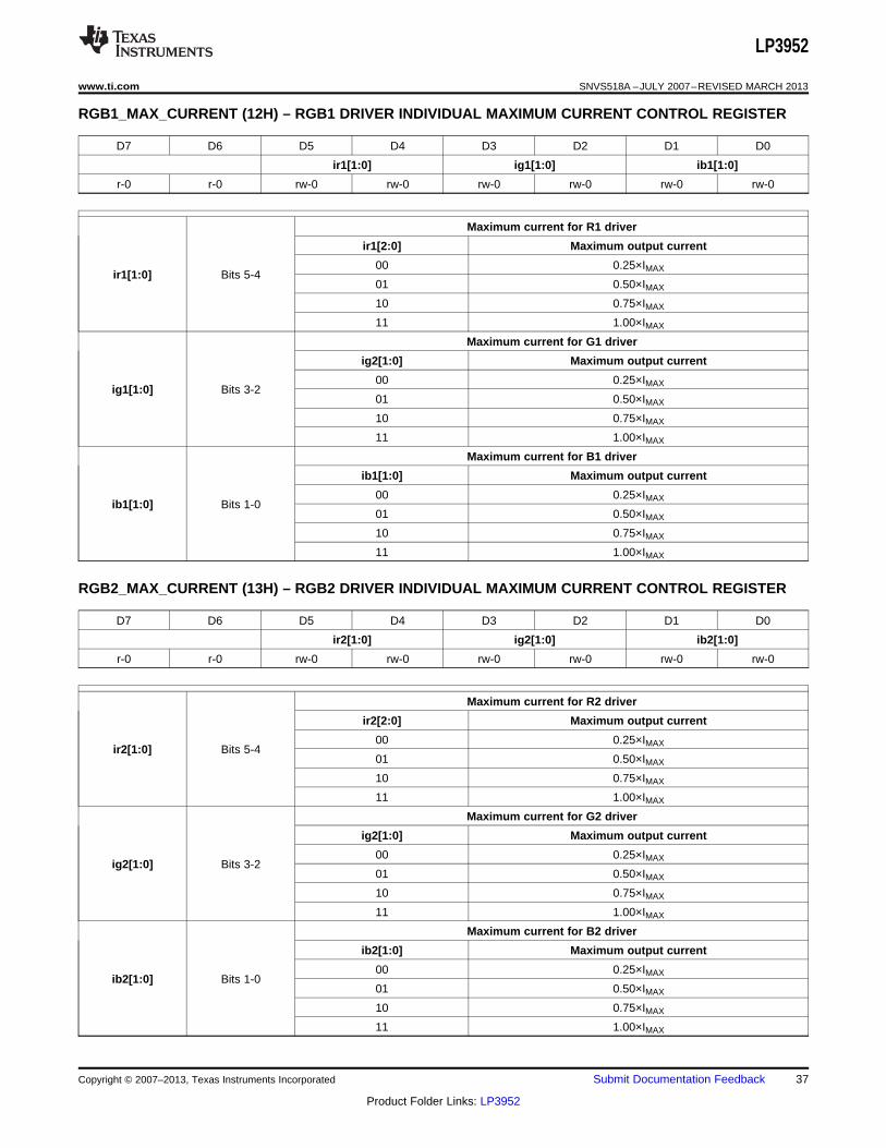
Both RGB output sets can be separately controlled as constant current sinks or as switches. This is done usingcc_rgb1/2 bits in the RGB control register. In constant current mode one or both RGB output sets are controlledwith constant current sinks (no external ballast resistors required). The maximum output current for both driversis set by one external resistor RRGB. User can decrease the maximum current for an individual LED driver byprogramming as shown later.
The maximum current for all RGB drivers is set with RRGB. The equation for calculating the maximum current is:IMAX = 100 × 1.23V / (RRGB + 50Ω) (1)
where:
IMAX - maximum RGB current in any RGB output in constant current mode
For example if 22mA is required for maximum RGB current RRGB equals to:RRGB=100×1.23V / IMAX–50Ω=123V / 0.022A–50Ω=5.54kΩ (2)
Each individual RGB output has a separate maximum current programming. The control bits are in registersRGB1 max current and RGB2 max current (12H and 13H) and programming is shown in table below. Thedefault value after reset is 00b.
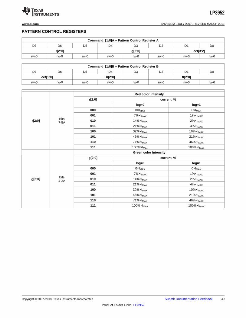
Command Based Pattern Generator for Color LEDs (1.65V ≤ VDDIO ≤ VDD1,2V) (unless otherwisenoted)
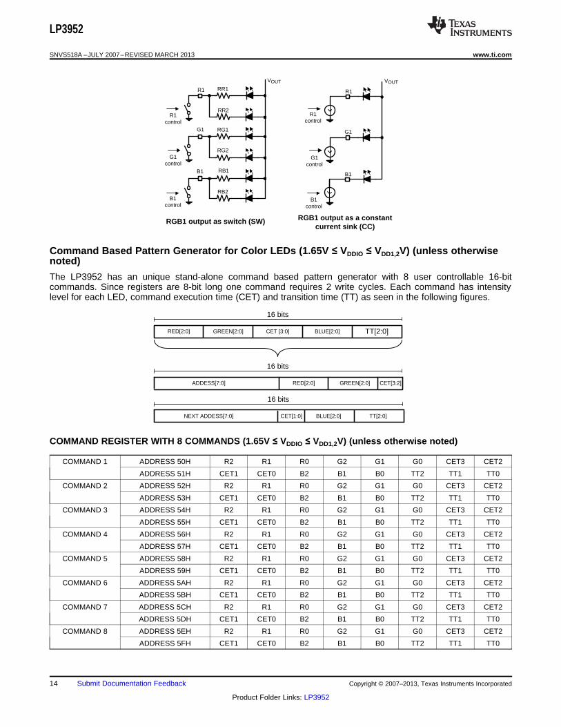
The LP3952 has an unique stand-alone command based pattern generator with 8 user controllable 16-bitcommands. Since registers are 8-bit long one command requires 2 write cycles. Each command has intensitylevel for each LED, command execution time (CET) and transition time (TT) as seen in the following figures.
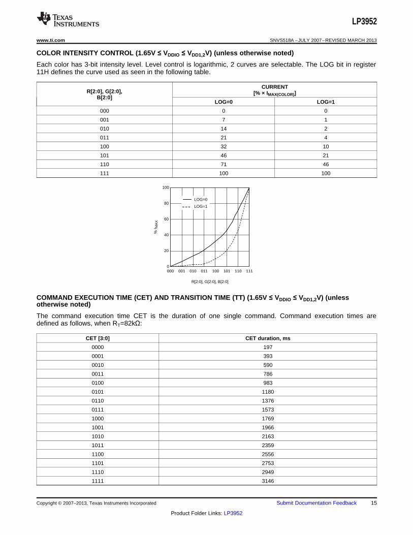
COLOR INTENSITY CONTROL (1.65V ≤ VDDIO ≤ VDD1,2V) (unless otherwise noted)
Each color has 3-bit intensity level. Level control is logarithmic, 2 curves are selectable. The LOG bit in register11H defines the curve used as seen in the following table.
CURRENTR[2:0], G[2:0], [% × IMAX(COLOR)]
B[2:0]LOG=0 LOG=1
000 0 0
001 7 1
010 14 2
011 21 4
100 32 10
101 46 21
110 71 46
111 100 100
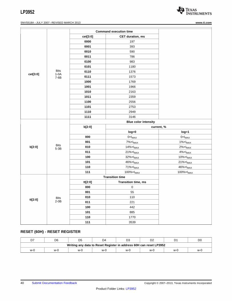
COMMAND EXECUTION TIME (CET) AND TRANSITION TIME (TT) (1.65V ≤ VDDIO ≤ VDD1,2V) (unlessotherwise noted)
The command execution time CET is the duration of one single command. Command execution times aredefined as follows, when RT=82kΩ:
Transition time TT is duration of transition from the previous RGB value to programmed new value. Transitiontimes are defined as follows:
TT [2:0] Transition time, ms
000 0
001 55
010 110
011 221
100 442
101 885
110 1770
111 3539
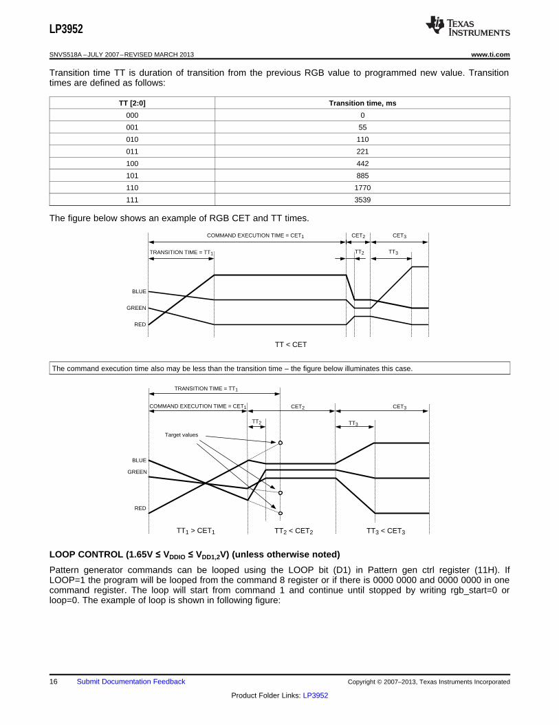
The figure below shows an example of RGB CET and TT times.
The command execution time also may be less than the transition time – the figure below illuminates this case.
LOOP CONTROL (1.65V ≤ VDDIO ≤ VDD1,2V) (unless otherwise noted)
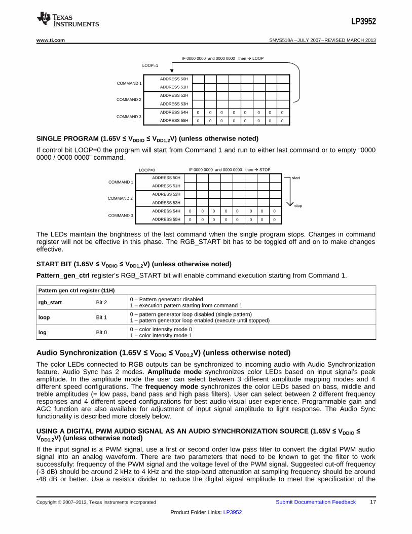
Pattern generator commands can be looped using the LOOP bit (D1) in Pattern gen ctrl register (11H). IfLOOP=1 the program will be looped from the command 8 register or if there is 0000 0000 and 0000 0000 in onecommand register. The loop will start from command 1 and continue until stopped by writing rgb_start=0 orloop=0. The example of loop is shown in following figure:
SINGLE PROGRAM (1.65V ≤ VDDIO ≤ VDD1,2V) (unless otherwise noted)
If control bit LOOP=0 the program will start from Command 1 and run to either last command or to empty “00000000 / 0000 0000” command.
The LEDs maintain the brightness of the last command when the single program stops. Changes in commandregister will not be effective in this phase. The RGB_START bit has to be toggled off and on to make changeseffective.
START BIT (1.65V ≤ VDDIO ≤ VDD1,2V) (unless otherwise noted)
Pattern_gen_ctrl register’s RGB_START bit will enable command execution starting from Command 1.
Pattern gen ctrl register (11H)
0 – Pattern generator disabledrgb_start Bit 2 1 – execution pattern starting from command 1
0 – pattern generator loop disabled (single pattern)loop Bit 1 1 – pattern generator loop enabled (execute until stopped)
0 – color intensity mode 0log Bit 0 1 – color intensity mode 1
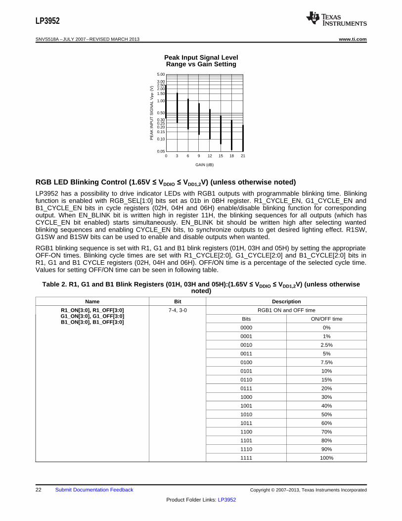
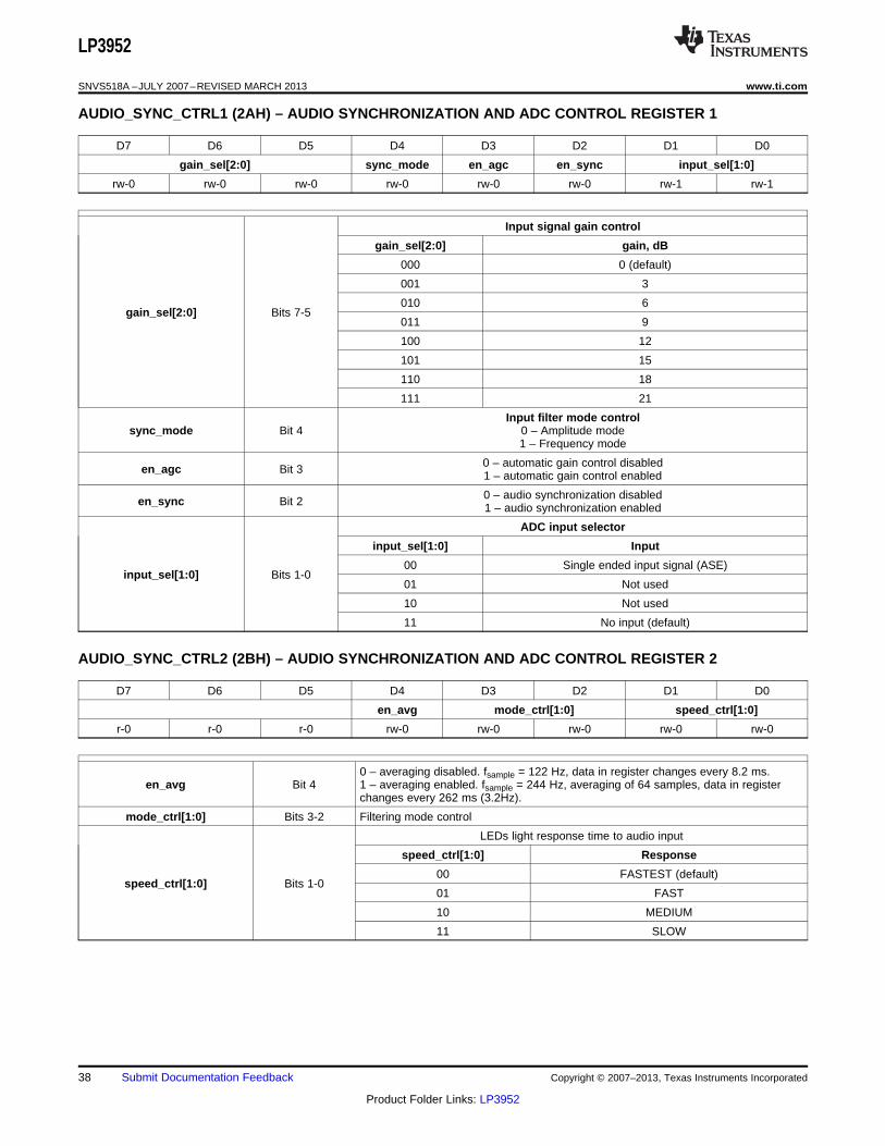
The color LEDs connected to RGB outputs can be synchronized to incoming audio with Audio Synchronizationfeature. Audio Sync has 2 modes. Amplitude mode synchronizes color LEDs based on input signal’s peakamplitude. In the amplitude mode the user can select between 3 different amplitude mapping modes and 4different speed configurations. The frequency mode synchronizes the color LEDs based on bass, middle andtreble amplitudes (= low pass, band pass and high pass filters). User can select between 2 different frequencyresponses and 4 different speed configurations for best audio-visual user experience. Programmable gain andAGC function are also available for adjustment of input signal amplitude to light response. The Audio Syncfunctionality is described more closely below.
USING A DIGITAL PWM AUDIO SIGNAL AS AN AUDIO SYNCHRONIZATION SOURCE (1.65V ≤ VDDIO ≤VDD1,2V) (unless otherwise noted)
If the input signal is a PWM signal, use a first or second order low pass filter to convert the digital PWM audiosignal into an analog waveform. There are two parameters that need to be known to get the filter to worksuccessfully: frequency of the PWM signal and the voltage level of the PWM signal. Suggested cut-off frequency(-3 dB) should be around 2 kHz to 4 kHz and the stop-band attenuation at sampling frequency should be around-48 dB or better. Use a resistor divider to reduce the digital signal amplitude to meet the specification of the
analog audio input. Because a low-order low-pass filter attenuates the high-frequency components from audiosignal, MODE_CTRL=01b selection is recommended when frequency synchronization mode is enabled.Application example 5 shows an example of a second order RC-filter for 29 kHz PWM signal with 3.3Vamplitude. Active filters, such as a Sallen-Key filter, may also be applied. An active filter gives better stop-bandattenuation and cut-off frequency can be higher than for a RC-filter.
To make sure that the filter rolls off sufficiently quickly, connect your filter circuit to the audio input(s), turn on theaudio synchronization feature, set manual gain to maximum, apply the PWM signal to the filter input and keep aneye on LEDs. If they are blinking without an audio signal (modulation), a sharper roll-off after the cut-offfrequency, more stop-band attenuation, or smaller amplitude of the PWM signal is required.
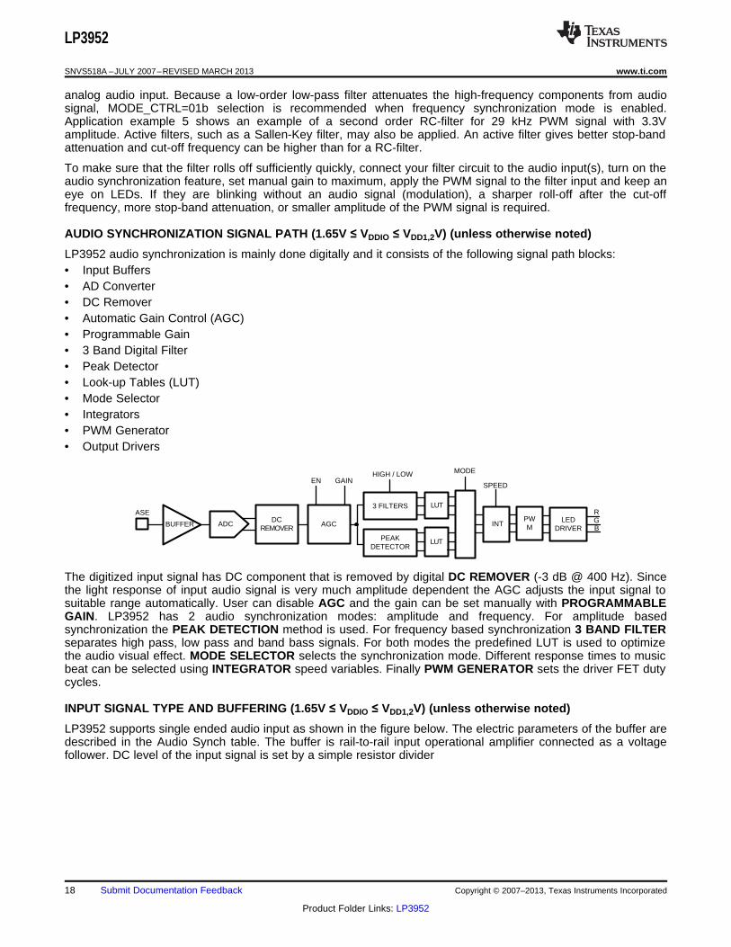
LP3952 audio synchronization is mainly done digitally and it consists of the following signal path blocks:• Input Buffers• AD Converter• DC Remover• Automatic Gain Control (AGC)• Programmable Gain• 3 Band Digital Filter• Peak Detector• Look-up Tables (LUT)• Mode Selector• Integrators• PWM Generator• Output Drivers
The digitized input signal has DC component that is removed by digital DC REMOVER (-3 dB @ 400 Hz). Sincethe light response of input audio signal is very much amplitude dependent the AGC adjusts the input signal tosuitable range automatically. User can disable AGC and the gain can be set manually with PROGRAMMABLEGAIN. LP3952 has 2 audio synchronization modes: amplitude and frequency. For amplitude basedsynchronization the PEAK DETECTION method is used. For frequency based synchronization 3 BAND FILTERseparates high pass, low pass and band bass signals. For both modes the predefined LUT is used to optimizethe audio visual effect. MODE SELECTOR selects the synchronization mode. Different response times to musicbeat can be selected using INTEGRATOR speed variables. Finally PWM GENERATOR sets the driver FET dutycycles.
INPUT SIGNAL TYPE AND BUFFERING (1.65V ≤ VDDIO ≤ VDD1,2V) (unless otherwise noted)
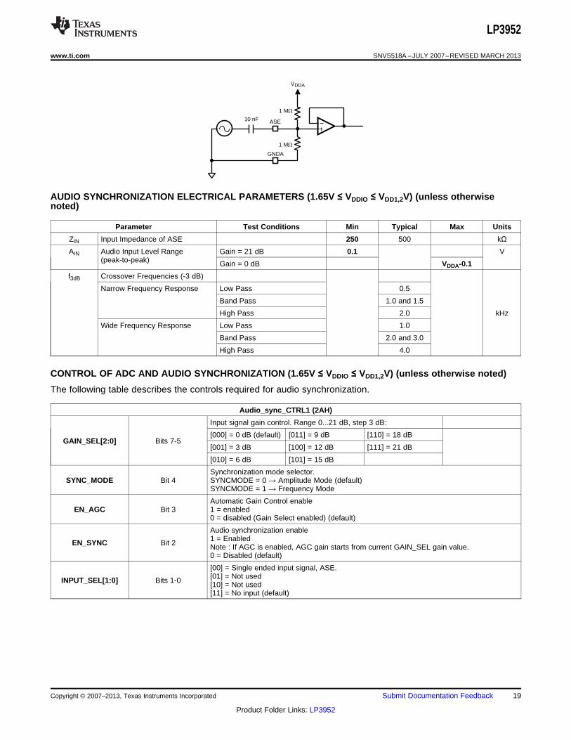
LP3952 supports single ended audio input as shown in the figure below. The electric parameters of the buffer aredescribed in the Audio Synch table. The buffer is rail-to-rail input operational amplifier connected as a voltagefollower. DC level of the input signal is set by a simple resistor divider
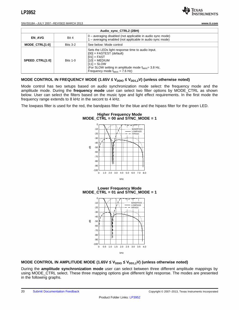
MODE CONTROL IN FREQUENCY MODE (1.65V ≤ VDDIO ≤ VDD1,2V) (unless otherwise noted)
Mode control has two setups based on audio synchronization mode select: the frequency mode and theamplitude mode. During the frequency mode user can select two filter options by MODE_CTRL as shownbelow. User can select the filters based on the music type and light effect requirements. In the first mode thefrequency range extends to 8 kHz in the secont to 4 kHz.
The lowpass filter is used for the red, the bandpass filter for the blue and the hipass filter for the green LED.
Higher Frequency ModeMODE_CTRL = 00 and SYNC_MODE = 1
Lower Frequency ModeMODE_CTRL = 01 and SYNC_MODE = 1
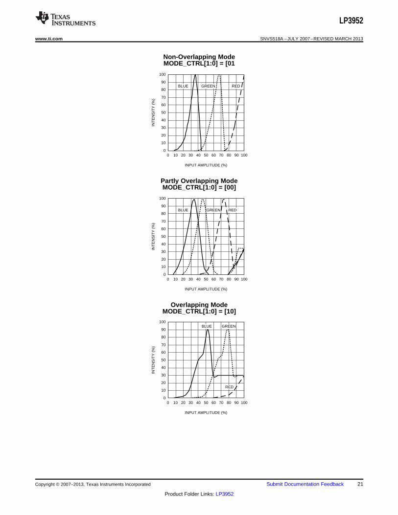
MODE CONTROL IN AMPLITUDE MODE (1.65V ≤ VDDIO ≤ VDD1,2V) (unless otherwise noted)
During the amplitude synchronization mode user can select between three different amplitude mappings byusing MODE_CTRL select. These three mapping options give different light response. The modes are presentedin the following graphs.
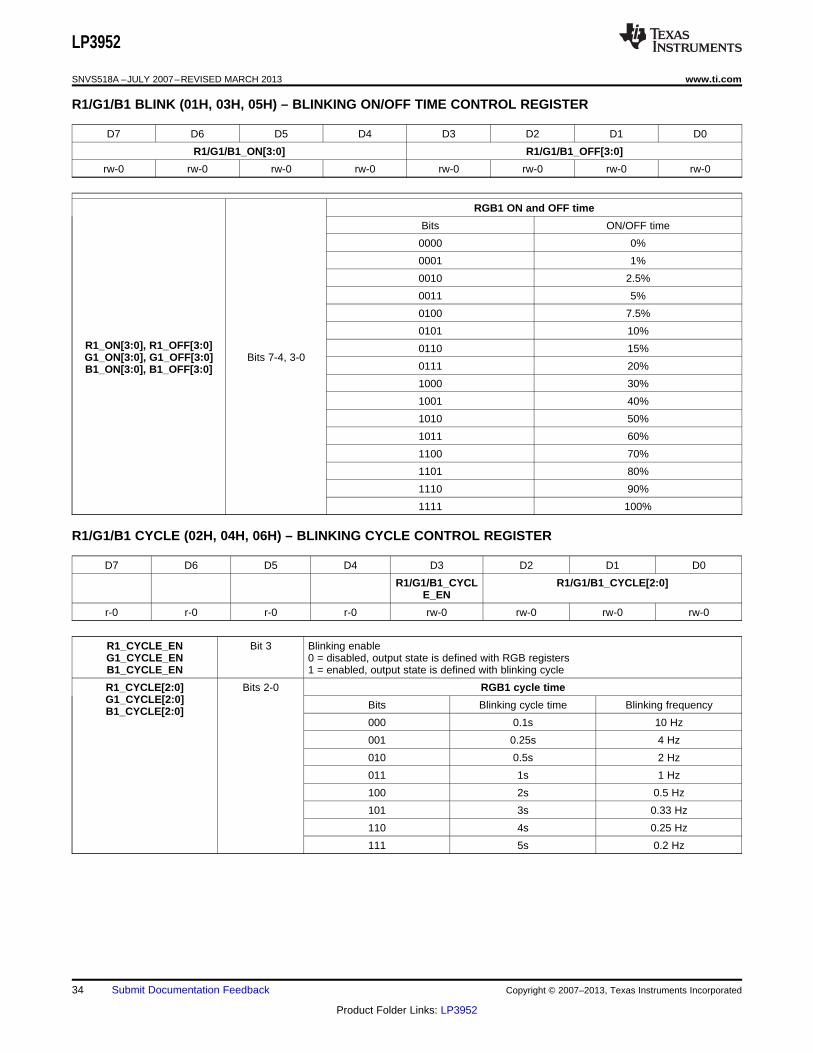
RGB LED Blinking Control (1.65V ≤ VDDIO ≤ VDD1,2V) (unless otherwise noted)
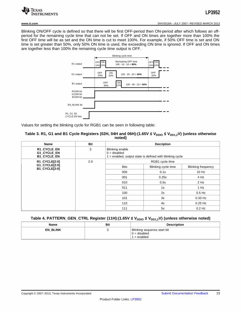
LP3952 has a possibility to drive indicator LEDs with RGB1 outputs with programmable blinking time. Blinkingfunction is enabled with RGB_SEL[1:0] bits set as 01b in 0BH register. R1_CYCLE_EN, G1_CYCLE_EN andB1_CYCLE_EN bits in cycle registers (02H, 04H and 06H) enable/disable blinking function for correspondingoutput. When EN_BLINK bit is written high in register 11H, the blinking sequences for all outputs (which hasCYCLE_EN bit enabled) starts simultaneously. EN_BLINK bit should be written high after selecting wantedblinking sequences and enabling CYCLE_EN bits, to synchronize outputs to get desired lighting effect. R1SW,G1SW and B1SW bits can be used to enable and disable outputs when wanted.
RGB1 blinking sequence is set with R1, G1 and B1 blink registers (01H, 03H and 05H) by setting the appropriateOFF-ON times. Blinking cycle times are set with R1_CYCLE[2:0], G1_CYCLE[2:0] and B1_CYCLE[2:0] bits inR1, G1 and B1 CYCLE registers (02H, 04H and 06H). OFF/ON time is a percentage of the selected cycle time.Values for setting OFF/ON time can be seen in following table.
Table 2. R1, G1 and B1 Blink Registers (01H, 03H and 05H):(1.65V ≤ VDDIO ≤ VDD1,2V) (unless otherwisenoted)
Name Bit Description
R1_ON[3:0], R1_OFF[3:0] 7-4, 3-0 RGB1 ON and OFF timeG1_ON[3:0], G1_OFF[3:0] Bits ON/OFF timeB1_ON[3:0], B1_OFF[3:0]
Blinking ON/OFF cycle is defined so that there will be first OFF-period then ON-period after which follows an off-period for the remaining cycle time that can not be set. If OFF and ON times are together more than 100% thefirst OFF time will be as set and the ON time is cut to meet 100%. For example, if 50% OFF time is set and ONtime is set greater than 50%, only 50% ON time is used, the exceeding ON time is ignored. If OFF and ON timesare together less than 100% the remaining cycle time output is OFF.
Values for setting the blinking cycle for RGB1 can be seen in following table:
Table 3. R1, G1 and B1 Cycle Registers (02H, 04H and 06H):(1.65V ≤ VDDIO ≤ VDD1,2V) (unless otherwisenoted)
Name Bit Decription
R1_CYCLE_EN 3 Blinking enableG1_CYCLE_EN 0 = disabledB1_CYCLE_EN 1 = enabled, output state is defined with blinking cycle
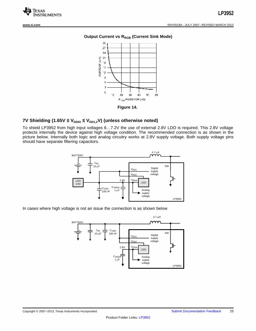
To shield LP3952 from high input voltages 6…7.2V the use of external 2.8V LDO is required. This 2.8V voltageprotects internally the device against high voltage condition. The recommended connection is as shown in thepicture below. Internally both logic and analog circuitry works at 2.8V supply voltage. Both supply voltage pinsshould have separate filtering capacitors.
In cases where high voltage is not an issue the connection is as shown below
Note: Any unused digital input pin has to be connected to GND to avoid floating and extra current consumption.
I2C Compatible Interface
INTERFACE BUS OVERVIEW
The I2C compatible synchronous serial interface provides access to the programmable functions and registers onthe device. This protocol uses a two-wire interface for bi-directional communications between the devicesconnected to the bus. The two interface lines are the Serial Data Line (SDA), and the Serial Clock Line (SCL).These lines should be connected to a positive supply, via a pull-up resistor and remain HIGH even when the busis idle. Every device on the bus is assigned a unique address and acts as either a Master or a Slave dependingon whether it generates or receives the serial clock (SCL).
DATA TRANSACTIONS
One data bit is transferred during each clock pulse. Data is sampled during the high state of the serial clock(SCL). Consequently, throughout the clock’s high period, the data should remain stable. Any changes on theSDA line during the high state of the SCL and in the middle of a transaction, aborts the current transaction. Newdata should be sent during the low SCL state. This protocol permits a single data line to transfer bothcommand/control information and data using the synchronous serial clock.
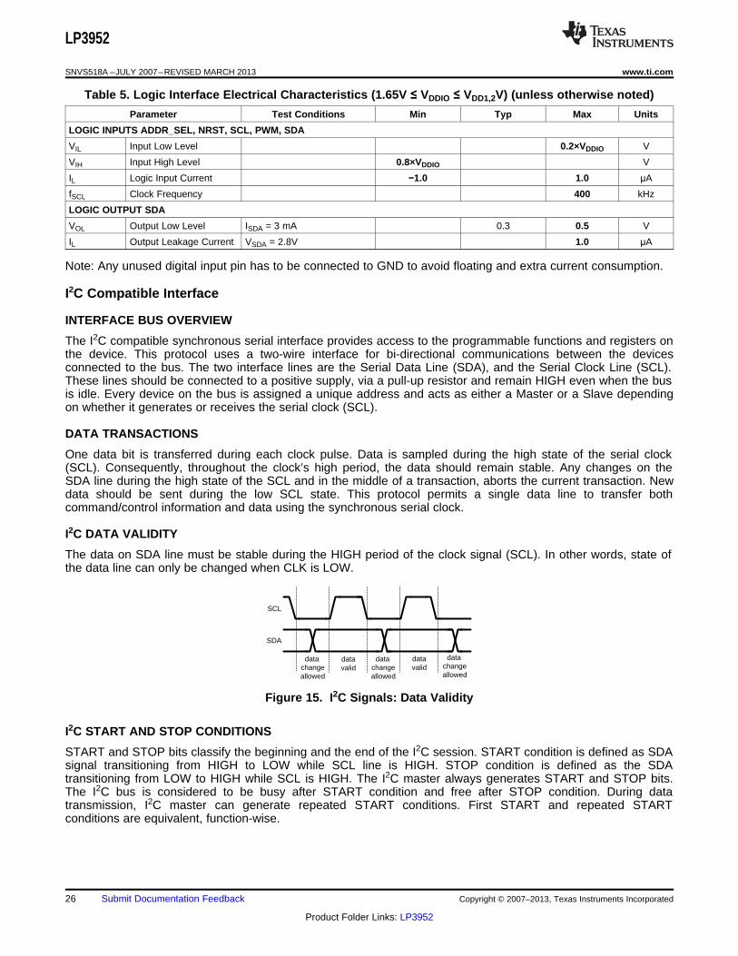
I2C DATA VALIDITY
The data on SDA line must be stable during the HIGH period of the clock signal (SCL). In other words, state ofthe data line can only be changed when CLK is LOW.
Figure 15. I2C Signals: Data Validity
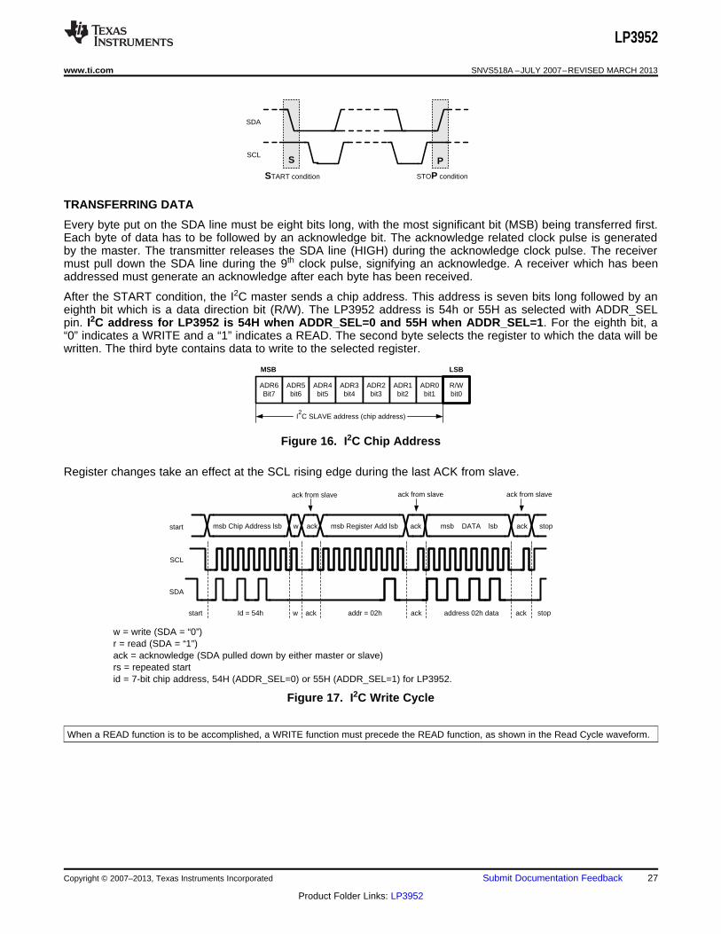
I2C START AND STOP CONDITIONS
START and STOP bits classify the beginning and the end of the I2C session. START condition is defined as SDAsignal transitioning from HIGH to LOW while SCL line is HIGH. STOP condition is defined as the SDAtransitioning from LOW to HIGH while SCL is HIGH. The I2C master always generates START and STOP bits.The I2C bus is considered to be busy after START condition and free after STOP condition. During datatransmission, I2C master can generate repeated START conditions. First START and repeated STARTconditions are equivalent, function-wise.
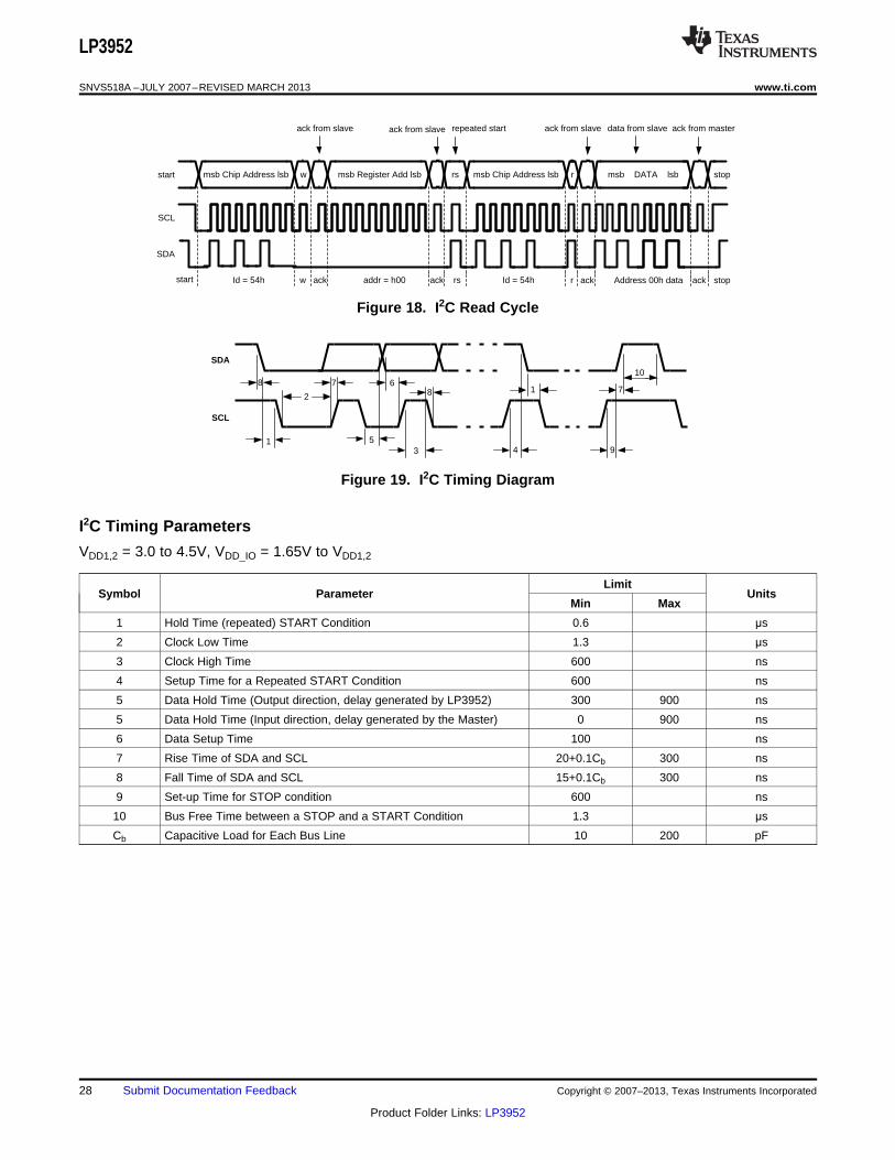
start msb Chip Address lsb w ack msb Register Add lsb ack msb DATA lsb ack stop
ack from slave ack from slave ack from slave
SCL
SDA
start Id = 54h w ack addr = 02h ack ackaddress 02h data stop
ADR6Bit7
ADR5bit6
ADR4bit5
ADR3bit4
ADR2bit3
ADR1bit2
ADR0bit1
R/Wbit0
MSB LSB
I2C SLAVE address (chip address)
SDA
SCLS P
START condition STOP condition
LP3952
www.ti.com SNVS518A –JULY 2007–REVISED MARCH 2013
TRANSFERRING DATA
Every byte put on the SDA line must be eight bits long, with the most significant bit (MSB) being transferred first.Each byte of data has to be followed by an acknowledge bit. The acknowledge related clock pulse is generatedby the master. The transmitter releases the SDA line (HIGH) during the acknowledge clock pulse. The receivermust pull down the SDA line during the 9th clock pulse, signifying an acknowledge. A receiver which has beenaddressed must generate an acknowledge after each byte has been received.
After the START condition, the I2C master sends a chip address. This address is seven bits long followed by aneighth bit which is a data direction bit (R/W). The LP3952 address is 54h or 55H as selected with ADDR_SELpin. I2C address for LP3952 is 54H when ADDR_SEL=0 and 55H when ADDR_SEL=1. For the eighth bit, a“0” indicates a WRITE and a “1” indicates a READ. The second byte selects the register to which the data will bewritten. The third byte contains data to write to the selected register.
Figure 16. I2C Chip Address
Register changes take an effect at the SCL rising edge during the last ACK from slave.
w = write (SDA = “0”)r = read (SDA = “1”)ack = acknowledge (SDA pulled down by either master or slave)rs = repeated startid = 7-bit chip address, 54H (ADDR_SEL=0) or 55H (ADDR_SEL=1) for LP3952.
Figure 17. I2C Write Cycle
When a READ function is to be accomplished, a WRITE function must precede the READ function, as shown in the Read Cycle waveform.
Autoincrement mode is available, with this mode it is possible to read or write bytes with autoincreasingaddresses. LP3952 has empty spaces in address register map, and it is recommended to use autoincrementmode only for writing in pattern command registers.
Recommended External Components
OUTPUT CAPACITOR, COUT
The output capacitor COUT directly affects the magnitude of the output ripple voltage. In general, the higher thevalue of COUT, the lower the output ripple magnitude. Multilayer ceramic capacitors with low ESR are the bestchoice. At the lighter loads, the low ESR ceramics offer a much lower Vout ripple that the higher ESR tantalumsof the same value. At the higher loads, the ceramics offer a slightly lower Vout ripple magnitude than thetantalums of the same value. However, the dv/dt of the Vout ripple with the ceramics is much lower than thetantalums under all load conditions. Capacitor voltage rating must be sufficient, 10V or greater is recommended.
Some ceramic capacitors, especially those in small packages, exhibit a strong capacitance reductionwith the increased applied DC voltage, so called DC bias effect. The capacitance value can fall to belowhalf of the nominal capacitance. Too low output capacitance will increase noise and it can make theboost converter unstable. Recommended maximum DC bias effect at 5V DC voltage is -50%.
INPUT CAPACITOR, CIN
The input capacitor CIN directly affects the magnitude of the input ripple voltage and to a lesser degree the VOUTripple. A higher value CIN will give a lower VIN ripple. Capacitor voltage rating must be sufficient, 10V or greater isrecommended.
OUTPUT DIODE, D1
A schottky diode should be used for the output diode. Peak repetitive current rating of the schottky diode shouldbe larger than the peak inductor current (ca. 1A). Average current rating of the schottky diode should be higherthan maximum output current used. Schottky diodes with a low forward drop and fast switching speeds are idealfor increasing efficiency in portable applications. Choose a reverse breakdown of the schottky diode larger thanthe output voltage. Do not use ordinary rectifier diodes, since slow switching speeds and long recovery timescause the efficiency and the load regulation to suffer.
INDUCTOR, L1
The LP3952’s high switching frequency enables the use of the small surface mount inductor. A 4.7 μH shieldedinductor is suggested for 2 MHz operation, 10 μH should be used at 1 MHz. The inductor should have asaturation current rating higher than the rms current it will experience during circuit operation. To get maximum(400 mA) current from the boost, an inductor with 1A saturation current is recommended. If output current is forexample 200 mA then inductor with 600 mA saturation current can be used. Less than 300 mΩ ESR issuggested for high efficiency. Open core inductors cause flux linkage with circuit components and interfere withthe normal operation of the circuit. This should be avoided. For high efficiency, choose an inductor with a highfrequency core material such as ferrite to reduce the core losses. The inductor should be connected to the SWpin as close to the IC as possible. Examples of suitable inductor for 400 mA output current is TDK VLF4012AT-4R7M1R1, and for 200mA application VLF3010AT-4R7MR70 or Panasonic ELLVEG4R7N.
LIST OF RECOMMENDED EXTERNAL COMPONENTS
Symbol Symbol explanation Value Unit Type
CVDD1 C between VDD1 and GND 100 nF Ceramic, X7R / X5R
CVDD2 C between VDD2 and GND 100 nF Ceramic, X7R / X5R
CVDDIO C between VDDIO and GND 100 nF Ceramic, X7R / X5R
CVDDA C between VDDA and GND 1 μF Ceramic, X7R / X5R
COUT C between FB and GND 10 μF Ceramic, X7R / X5R, 10V
CIN C between battery voltage and GND 10 μF Ceramic, X7R / X5R
L1 L between SW and VBAT at 2 MHz 4.7 μH Shielded, low ESR, Isat=1A for 400mA output current, Isat=600 mA for200 mA output current
CVDDIO C between VDDIO and GND 100 nF Ceramic, X7R
RRBG R between IRGB and GND 5.6 kΩ ±1%
RRT R between IRT and GND 82 kΩ ±1%
D1 Rectifying Diode (Vf @ maxload) 0.3 V Schottky diode
CASE C between Audio input and ASE 100 nF Ceramic, X7R / X5R
LEDs User defined
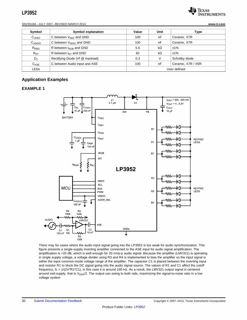
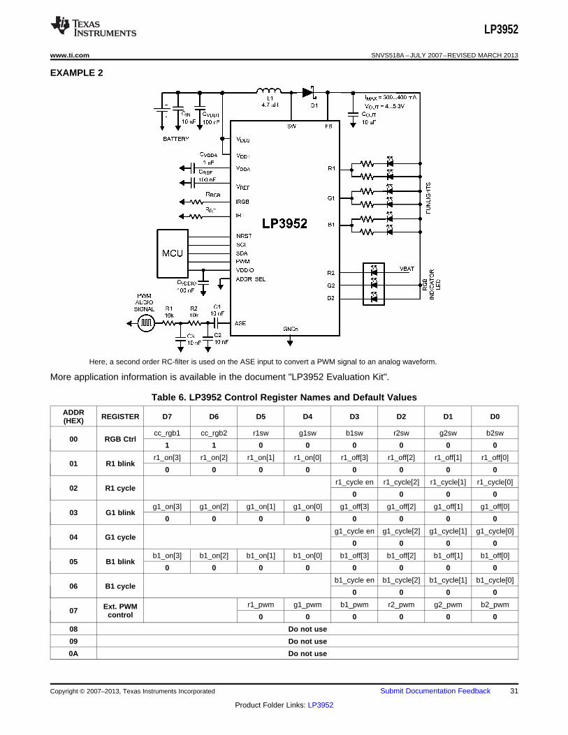
Application Examples
EXAMPLE 1
There may be cases where the audio input signal going into the LP3952 is too weak for audio synchronization. Thisfigure presents a single-supply inverting amplifier connected to the ASE input for audio signal amplification. Theamplification is +20 dB, which is well enough for 20 mVp-p audio signal. Because the amplifier (LMV321) is operatingin single supply voltage, a voltage divider using R3 and R4 is implemented to bias the amplifier so the input signal iswithin the input common-mode voltage range of the amplifier. The capacitor C1 is placed between the inverting inputand resistor R1 to block the DC signal going into the audio signal source. The values of R1 and C1 affect the cutofffrequency, fc = 1/(2π*R1*C1), in this case it is around 160 Hz. As a result, the LMV321 output signal is centeredaround mid-supply, that is VDDA/2. The output can swing to both rails, maximizing the signal-to-noise ratio in a lowvoltage system
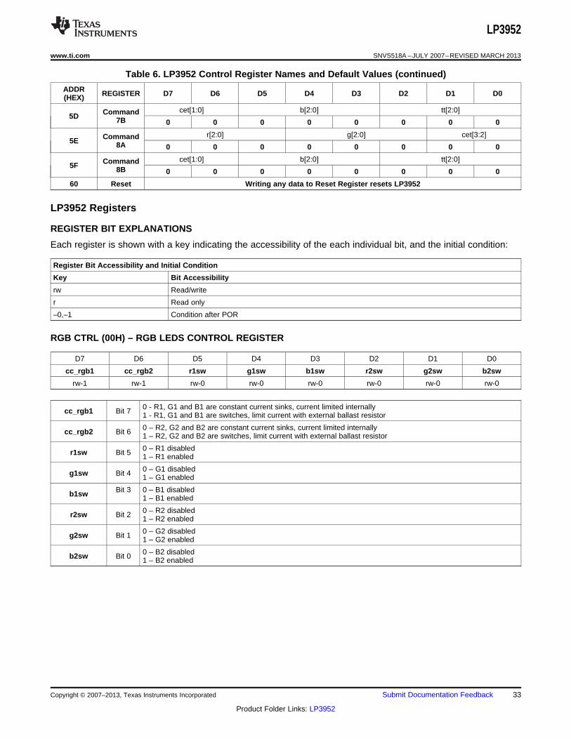
60 Reset Writing any data to Reset Register resets LP3952
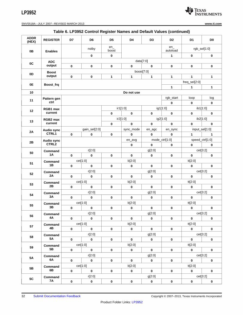
LP3952 Registers
REGISTER BIT EXPLANATIONS
Each register is shown with a key indicating the accessibility of the each individual bit, and the initial condition:
Register Bit Accessibility and Initial Condition
Key Bit Accessibility
rw Read/write
r Read only
–0,–1 Condition after POR
RGB CTRL (00H) – RGB LEDS CONTROL REGISTER
D7 D6 D5 D4 D3 D2 D1 D0
cc_rgb1 cc_rgb2 r1sw g1sw b1sw r2sw g2sw b2sw
rw-1 rw-1 rw-0 rw-0 rw-0 rw-0 rw-0 rw-0
0 - R1, G1 and B1 are constant current sinks, current limited internallycc_rgb1 Bit 7 1 - R1, G1 and B1 are switches, limit current with external ballast resistor
0 – R2, G2 and B2 are constant current sinks, current limited internallycc_rgb2 Bit 6 1 – R2, G2 and B2 are switches, limit current with external ballast resistor
R1/G1/B1 CYCLE (02H, 04H, 06H) – BLINKING CYCLE CONTROL REGISTER
D7 D6 D5 D4 D3 D2 D1 D0
R1/G1/B1_CYCL R1/G1/B1_CYCLE[2:0]E_EN
r-0 r-0 r-0 r-0 rw-0 rw-0 rw-0 rw-0
R1_CYCLE_EN Bit 3 Blinking enableG1_CYCLE_EN 0 = disabled, output state is defined with RGB registersB1_CYCLE_EN 1 = enabled, output state is defined with blinking cycle
00 Single ended input signal (ASE)input_sel[1:0] Bits 1-0
01 Not used
10 Not used
11 No input (default)
AUDIO_SYNC_CTRL2 (2BH) – AUDIO SYNCHRONIZATION AND ADC CONTROL REGISTER 2
D7 D6 D5 D4 D3 D2 D1 D0
en_avg mode_ctrl[1:0] speed_ctrl[1:0]
r-0 r-0 r-0 rw-0 rw-0 rw-0 rw-0 rw-0
0 – averaging disabled. fsample = 122 Hz, data in register changes every 8.2 ms.en_avg Bit 4 1 – averaging enabled. fsample = 244 Hz, averaging of 64 samples, data in register
Changes from Original (March 2013) to Revision A Page
• Changed layout of National Data Sheet to TI format .......................................................................................................... 40
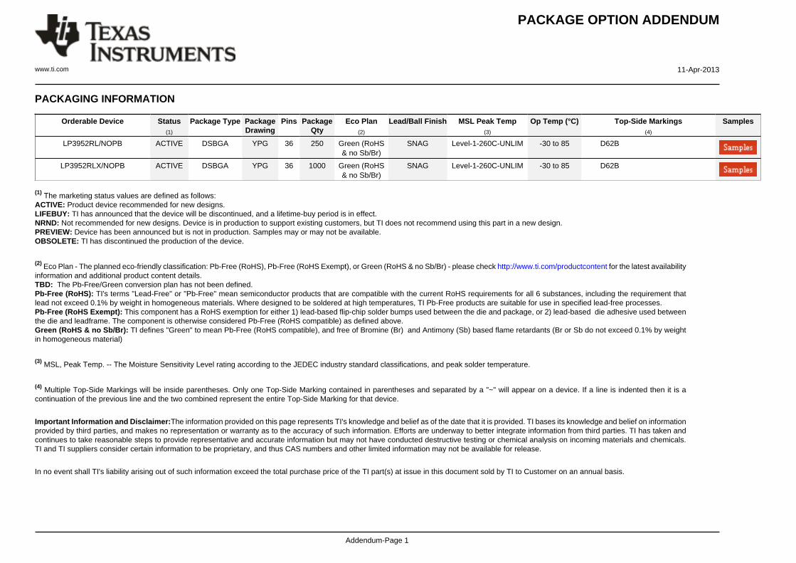
LP3952RL/NOPB ACTIVE DSBGA YPG 36 250 Green (RoHS& no Sb/Br)
SNAG Level-1-260C-UNLIM -30 to 85 D62B
LP3952RLX/NOPB ACTIVE DSBGA YPG 36 1000 Green (RoHS& no Sb/Br)
SNAG Level-1-260C-UNLIM -30 to 85 D62B
(1) The marketing status values are defined as follows:ACTIVE: Product device recommended for new designs.LIFEBUY: TI has announced that the device will be discontinued, and a lifetime-buy period is in effect.NRND: Not recommended for new designs. Device is in production to support existing customers, but TI does not recommend using this part in a new design.PREVIEW: Device has been announced but is not in production. Samples may or may not be available.OBSOLETE: TI has discontinued the production of the device.
(2) Eco Plan - The planned eco-friendly classification: Pb-Free (RoHS), Pb-Free (RoHS Exempt), or Green (RoHS & no Sb/Br) - please check http://www.ti.com/productcontent for the latest availabilityinformation and additional product content details.TBD: The Pb-Free/Green conversion plan has not been defined.Pb-Free (RoHS): TI's terms "Lead-Free" or "Pb-Free" mean semiconductor products that are compatible with the current RoHS requirements for all 6 substances, including the requirement thatlead not exceed 0.1% by weight in homogeneous materials. Where designed to be soldered at high temperatures, TI Pb-Free products are suitable for use in specified lead-free processes.Pb-Free (RoHS Exempt): This component has a RoHS exemption for either 1) lead-based flip-chip solder bumps used between the die and package, or 2) lead-based die adhesive used betweenthe die and leadframe. The component is otherwise considered Pb-Free (RoHS compatible) as defined above.Green (RoHS & no Sb/Br): TI defines "Green" to mean Pb-Free (RoHS compatible), and free of Bromine (Br) and Antimony (Sb) based flame retardants (Br or Sb do not exceed 0.1% by weightin homogeneous material)
(3) MSL, Peak Temp. -- The Moisture Sensitivity Level rating according to the JEDEC industry standard classifications, and peak solder temperature.
(4) Multiple Top-Side Markings will be inside parentheses. Only one Top-Side Marking contained in parentheses and separated by a "~" will appear on a device. If a line is indented then it is acontinuation of the previous line and the two combined represent the entire Top-Side Marking for that device.
Important Information and Disclaimer:The information provided on this page represents TI's knowledge and belief as of the date that it is provided. TI bases its knowledge and belief on informationprovided by third parties, and makes no representation or warranty as to the accuracy of such information. Efforts are underway to better integrate information from third parties. TI has taken andcontinues to take reasonable steps to provide representative and accurate information but may not have conducted destructive testing or chemical analysis on incoming materials and chemicals.TI and TI suppliers consider certain information to be proprietary, and thus CAS numbers and other limited information may not be available for release.
In no event shall TI's liability arising out of such information exceed the total purchase price of the TI part(s) at issue in this document sold by TI to Customer on an annual basis.
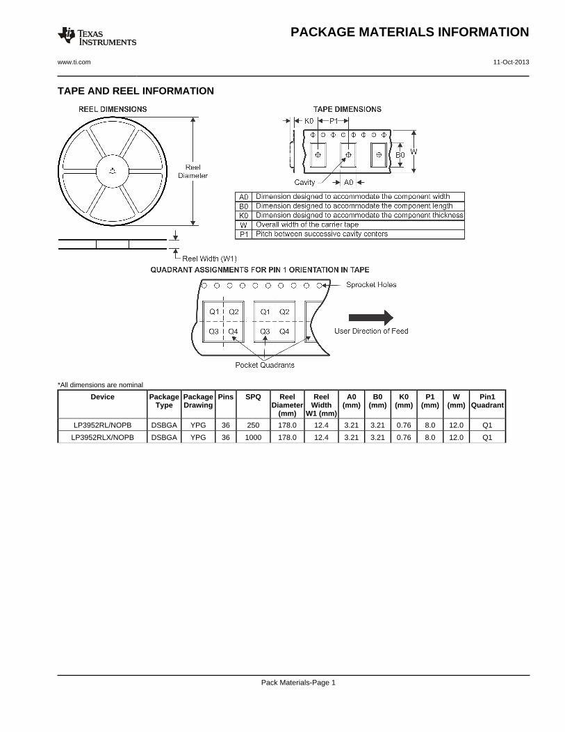
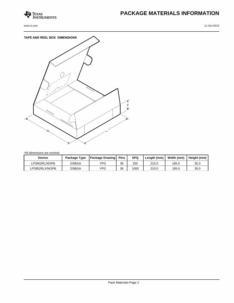
A. All linear dimensions are in millimeters. Dimensioning and tolerancing per ASME Y14.5M-1994. B. This drawing is subject to change without notice.
NOTES:
D: Max =
E: Max =
3.013 mm, Min =
3.013 mm, Min =
2.952 mm
2.952 mm
IMPORTANT NOTICE
Texas Instruments Incorporated and its subsidiaries (TI) reserve the right to make corrections, enhancements, improvements and otherchanges to its semiconductor products and services per JESD46, latest issue, and to discontinue any product or service per JESD48, latestissue. Buyers should obtain the latest relevant information before placing orders and should verify that such information is current andcomplete. All semiconductor products (also referred to herein as “components”) are sold subject to TI’s terms and conditions of salesupplied at the time of order acknowledgment.
TI warrants performance of its components to the specifications applicable at the time of sale, in accordance with the warranty in TI’s termsand conditions of sale of semiconductor products. Testing and other quality control techniques are used to the extent TI deems necessaryto support this warranty. Except where mandated by applicable law, testing of all parameters of each component is not necessarilyperformed.
TI assumes no liability for applications assistance or the design of Buyers’ products. Buyers are responsible for their products andapplications using TI components. To minimize the risks associated with Buyers’ products and applications, Buyers should provideadequate design and operating safeguards.
TI does not warrant or represent that any license, either express or implied, is granted under any patent right, copyright, mask work right, orother intellectual property right relating to any combination, machine, or process in which TI components or services are used. Informationpublished by TI regarding third-party products or services does not constitute a license to use such products or services or a warranty orendorsement thereof. Use of such information may require a license from a third party under the patents or other intellectual property of thethird party, or a license from TI under the patents or other intellectual property of TI.
Reproduction of significant portions of TI information in TI data books or data sheets is permissible only if reproduction is without alterationand is accompanied by all associated warranties, conditions, limitations, and notices. TI is not responsible or liable for such altereddocumentation. Information of third parties may be subject to additional restrictions.
Resale of TI components or services with statements different from or beyond the parameters stated by TI for that component or servicevoids all express and any implied warranties for the associated TI component or service and is an unfair and deceptive business practice.TI is not responsible or liable for any such statements.
Buyer acknowledges and agrees that it is solely responsible for compliance with all legal, regulatory and safety-related requirementsconcerning its products, and any use of TI components in its applications, notwithstanding any applications-related information or supportthat may be provided by TI. Buyer represents and agrees that it has all the necessary expertise to create and implement safeguards whichanticipate dangerous consequences of failures, monitor failures and their consequences, lessen the likelihood of failures that might causeharm and take appropriate remedial actions. Buyer will fully indemnify TI and its representatives against any damages arising out of the useof any TI components in safety-critical applications.
In some cases, TI components may be promoted specifically to facilitate safety-related applications. With such components, TI’s goal is tohelp enable customers to design and create their own end-product solutions that meet applicable functional safety standards andrequirements. Nonetheless, such components are subject to these terms.
No TI components are authorized for use in FDA Class III (or similar life-critical medical equipment) unless authorized officers of the partieshave executed a special agreement specifically governing such use.
Only those TI components which TI has specifically designated as military grade or “enhanced plastic” are designed and intended for use inmilitary/aerospace applications or environments. Buyer acknowledges and agrees that any military or aerospace use of TI componentswhich have not been so designated is solely at the Buyer's risk, and that Buyer is solely responsible for compliance with all legal andregulatory requirements in connection with such use.
TI has specifically designated certain components as meeting ISO/TS16949 requirements, mainly for automotive use. In any case of use ofnon-designated products, TI will not be responsible for any failure to meet ISO/TS16949.
Products Applications
Audio www.ti.com/audio Automotive and Transportation www.ti.com/automotive
Amplifiers amplifier.ti.com Communications and Telecom www.ti.com/communications
Data Converters dataconverter.ti.com Computers and Peripherals www.ti.com/computers