An IMPORTANT NOTICE at the end of this data sheet addresses availability, warranty, changes, use in safety-critical applications,intellectual property matters and other important disclaimers. PRODUCTION DATA.
LP5521SNVS441I –JANUARY 2007–REVISED NOVEMBER 2016
LP5521 Three-Channel RGB, White-LED Driver With Internal Program Memory andIntegrated Charge Pump
1
1 Features1• Adaptive Charge Pump With 1× and 1.5× Gain
Provides Up to 95% LED Drive Efficiency• Charge Pump with Soft Start and Overcurrent,
Short-Circuit Protection• Low Input Ripple and EMI• Very Small Solution Size, No Inductor or Resistors
Required• 200-nA Typical Shutdown Current• Automatic Power Save Mode• I2C-Compatible Interface• Independently Programmable Constant Current
Outputs with 8-Bit Current Setting and 8-Bit PWMControl
• Typical LED Output Saturation Voltage 50 mV andCurrent Matching 1%
• Three Program Execution Engines with FlexibleInstruction Set
• Autonomous Operation Without External Control• Large SRAM Program Memory• Two General Purpose Digital Outputs
2 Applications• Fun and Indicator Lights• LCD Sub-Display Backlighting• Keypad RGB Backlighting and Phone Cosmetics• Vibra, Speakers, Waveform Generator• Blood Glucose Meter• Handheld POS Terminals• Electronic Access Control• Where RGB Indication is Needed
Typical Application Circuit
3 DescriptionThe LP5521 is a three-channel LED driver designedto produce variety of lighting effects for mobiledevices. A high-efficiency charge pump enables LEDdriving over full Li-Ion battery voltage range. Thedevice has a program memory for creating variety oflighting sequences. When program memory has beenloaded, LP5521 can operate autonomously withoutprocessor control allowing power savings.
The device maintains excellent efficiency over a wideoperating range by automatically selecting propercharge pump gain based on LED forward voltagerequirements and is able to automatically enterpower-save mode, when LED outputs are not activeand thus lowering current consumption.
Three independent LED channels have accurateprogrammable current sources and PWM control.Each channel has program memory for creatingdesired lighting sequences with PWM control.
The LP5521 has a flexible digital interface. TriggerI/O and a 32-kHz clock input allow synchronizationbetween multiple devices. Interrupt output can beused to notify processor, when LED sequence hasended. The LP5521 has four pin selectable I2C-compatible addresses. This allows connecting up tofour parallel devices in one I2C-compatible bus. GPOand INT pins can be used as a digital control pin forother devices.
The LP5521 requires only four small, low-costceramic capacitors.
Comprehensive application tools are available,including command compiler for easy LED sequenceprogramming.
Device Information(1)
PART NUMBER PACKAGE BODY SIZELP5521TM DSBGA (20) 2.093 mm × 1.733 mm (MAX)LP5521YQ WQFN (24) 5.00 mm × 4.00 mm (NOM)
(1) For all available packages, see the orderable addendum atthe end of the data sheet.
9 Power Supply Recommendations ...................... 4010 Layout................................................................... 40
10.1 Layout Guidelines ................................................. 4010.2 Layout Example .................................................... 40
11 Device and Documentation Support ................. 4111.1 Device Support...................................................... 4111.2 Documentation Support ........................................ 4111.3 Receiving Notification of Documentation Updates 4111.4 Community Resources.......................................... 4111.5 Trademarks ........................................................... 4111.6 Electrostatic Discharge Caution............................ 4111.7 Glossary ................................................................ 41
12 Mechanical, Packaging, and OrderableInformation ........................................................... 41
4 Revision History
Changes from Revision H (May 2016) to Revision I Page
• Changed wording of title ........................................................................................................................................................ 1
Changes from Revision G (September 2014) to Revision H Page
• Added several new Applications ............................................................................................................................................ 1• Changed Body Size of DSBGA package to MAX dimensions .............................................................................................. 1• Changed Handling Ratings to ESD Ratings table ................................................................................................................. 5• Changed RθJA value for DSBGA from 50 – 90°C/W to 70.7°C/W and WQFN from 37 – 90°C/W to 38.4°C/W; add
additional thermal information ................................................................................................................................................ 6• Added Community Resources ............................................................................................................................................. 41
Changes from Revision F (February 2013) to Revision G Page
• Added Pin Configuration and Functions section, Handling Rating table, Feature Description section, DeviceFunctional Modes, Application and Implementation section, Power Supply Recommendations section, Layoutsection, Device and Documentation Support section, and Mechanical, Packaging, and Orderable Informationsection ................................................................................................................................................................................... 1
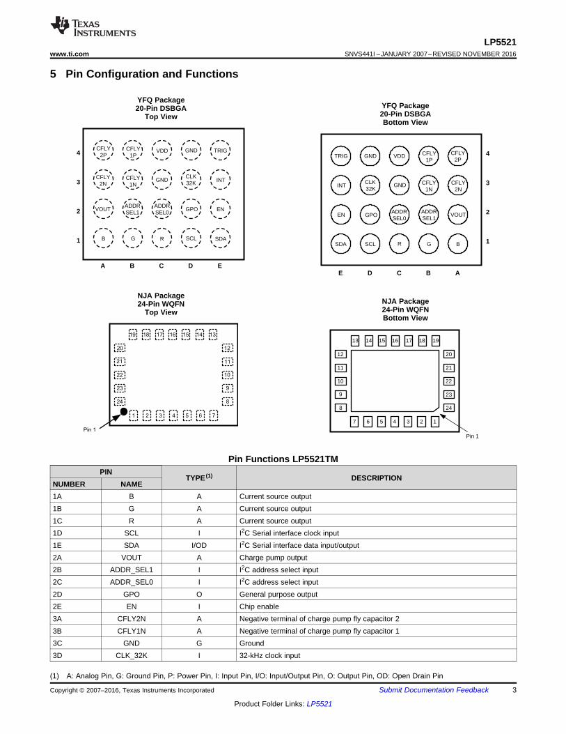
(1) A: Analog Pin, G: Ground Pin, P: Power Pin, I: Input Pin, I/O: Input/Output Pin, O: Output Pin, OD: Open Drain Pin
Pin Functions LP5521TMPIN
TYPE (1) DESCRIPTIONNUMBER NAME1A B A Current source output1B G A Current source output1C R A Current source output1D SCL I I2C Serial interface clock input1E SDA I/OD I2C Serial interface data input/output2A VOUT A Charge pump output2B ADDR_SEL1 I I2C address select input2C ADDR_SEL0 I I2C address select input2D GPO O General purpose output2E EN I Chip enable3A CFLY2N A Negative terminal of charge pump fly capacitor 23B CFLY1N A Negative terminal of charge pump fly capacitor 13C GND G Ground3D CLK_32K I 32-kHz clock input
TYPE (1) DESCRIPTIONNUMBER NAME3E INT OD/O Interrupt output / General Purpose Output4A CFLY2P A Positive terminal of charge pump fly capacitor 24B CFLY1P A Positive terminal of charge pump fly capacitor 14C VDD P Power supply pin4D GND G Ground4E TRIG I/OD Trigger input/output
(1) A: Analog Pin, G: Ground Pin, P: Power Pin, I: Input Pin, I/O: Input/Output Pin, O: Output Pin, OD: Open Drain Pin
Pin Functions LP5521YQPIN
TYPE (1) DESCRIPTIONNUMBER NAME1 CFLY2P A Positive pin of charge pump fly capacitor 22 CFLY1P A Positive pin of charge pump fly capacitor 13 VDD P Power supply pin4 GND G Ground5 CLK_32K I 32-kHz clock input6 INT OD/O Interrupt output / General purpose output7 TRIG I/OD Trigger input/output8 N/C9 N/C10 N/C11 N/C12 N/C13 SDA I/OD I2C serial interface data input/output14 EN I Chip enable15 SCL I I2C Serial interface clock input16 GPO O General purpose output17 R A Current source output18 G A Current source output19 B A Current source output20 ADDR_SEL0 I I2C address select input21 ADDR_SEL1 I I2C address select input22 VOUT A Charge pump output23 CFLY2N A Negative pin of charge pump fly capacitor 224 CFLY1N A Negative pin of charge pump fly capacitor 1
(1) Stresses beyond those listed under Absolute Maximum Ratings may cause permanent damage to the device. These are stress ratingsonly, and functional operation of the device at these or any other conditions beyond those indicated under Recommended OperatingConditions is not implied. Exposure to absolute-maximum-rated conditions for extended periods may affect device reliability.
(2) All voltages are with respect to the potential at the GND pins.(3) If Military/Aerospace specified devices are required, contact the Texas Instruments Sales Office/ Distributors for availability and
specifications.(4) Internal thermal shutdown circuitry protects the device from permanent damage. Thermal shutdown engages at TJ = 150°C (typical) and
disengages at TJ = 130°C (typical).(5) For detailed soldering specifications and information, please refer to DSBGA Wafer Level Chip Scale Package (SNVA009) or Leadless
Leadframe Package (LLP) (SNOA401).
6 Specifications
6.1 Absolute Maximum Ratingsover operating free-air temperature range (unless otherwise noted) (1) (2) (2) (3)
MIN MAX UNITV (VDD , VOUT, R, G, B) –0.3 6 VVoltage on logic pins –0.3 VDD + 0.3 with 6 V maximum VContinuous power dissipation (4) Internally LimitedJunction temperature, TJ-MAX 125 °CMaximum lead temperature (soldering) See (5)
Storage temperature, Tstg –65 150 °C
(1) JEDEC document JEP155 states that 500-V HBM allows safe manufacturing with a standard ESD control process.(2) JEDEC document JEP157 states that 250-V CDM allows safe manufacturing with a standard ESD control process.
6.2 ESD RatingsVALUE UNIT
V(ESD) Electrostatic dischargeHuman-body model (HBM), per ANSI/ESDA/JEDEC JS-001 (1) ±2000
VCharged-device model (CDM), per JEDEC specification JESD22-C101 (2) ±200
(1) Stresses beyond those listed under Absolute Maximum Ratings may cause permanent damage to the device. These are stress ratingsonly, and functional operation of the device at these or any other conditions beyond those indicated under Recommended OperatingConditions is not implied. Exposure to absolute-maximum-rated conditions for extended periods may affect device reliability.
(2) All voltages are with respect to the potential at the GND pins.(3) In applications where high power dissipation and/or poor package thermal resistance is present, the maximum ambient temperature may
have to be derated. Maximum ambient temperature (TA-MAX) is dependent on the maximum operating junction temperature (TJ-MAX-OP =125°C), the maximum power dissipation of the device in the application (PD-MAX), and the junction-to ambient thermal resistance of thepart/package in the application (RθJA), as given by the following equation: TA-MAX = TJ-MAX-OP – (RθJA × PD-MAX).
6.3 Recommended Operating Conditionsover operating free-air temperature range (unless otherwise noted) (1) (2) (2)
MIN MAX UNITVDD 2.7 5.5 VRecommended charge pump load current IOUT 0 100 mAJunction temperature, TJ, –30 125 °CAmbient temperature, TA
(1) All voltages are with respect to the potential at the GND pins.(2) Minimum and Maximum limits are specified by design, test, or statistical analysis.(3) Low-ESR Surface-Mount Ceramic Capacitors (MLCCs) used in setting electrical characteristics.
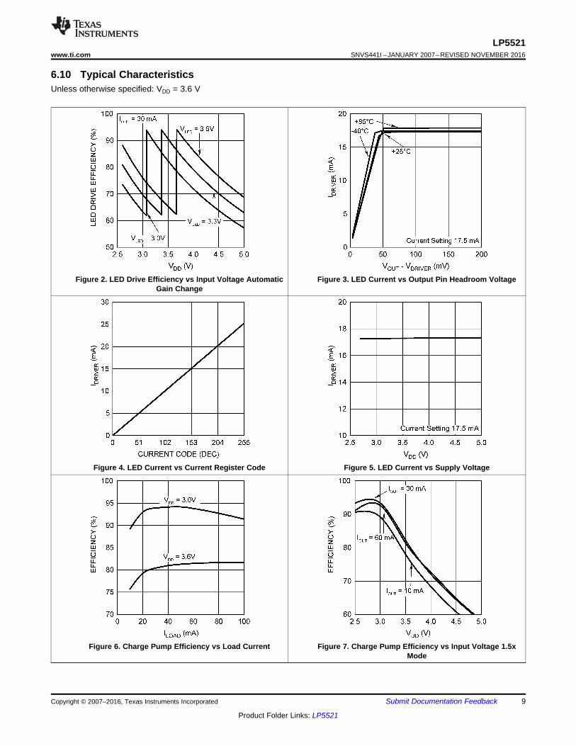
6.5 Electrical CharacteristicsUnless otherwise noted, specifications apply to the LP5521 Functional Block Diagram with: 2.7 V ≤ VDD ≤ 5.5 V, COUT= CIN =1 μF, CFLY1 = CFLY2 = 0.47 μF; limits are for TJ = 25°C unless specified in the test conditions. (1) (2) (3)
SYMBOL PARAMETER TEST CONDITIONS MIN TYP MAX UNIT
IVDD
Standby supply current EN = 0 (pin), CHIP_EN = 0 (bit), external 32kHz clock running or not running 0.2
μAEN = 0 (pin), CHIP_EN = 0 (bit), external 32-kHz clock running or not running, –30°C < TA <85°C
2
EN = 1 (pin), CHIP_EN = 0 (bit), external 32-kHz clock not running
(1) Input, output, and fly capacitors should be of the type X5R or X7R low ESR ceramic capacitor.
6.6 Charge Pump Electrical CharacteristicsLimits are for TJ = 25°C unless specified in the test conditions. (1)
SYMBOL PARAMETER TEST CONDITION MIN TYP MAX UNITROUT Charge pump output
resistanceGain = 1.5× 3.5 ΩGain = 1× 1 Ω
fSW Switching frequency 1.25 MHz–30°C < TA < 85°C –7% 7%
IGND Ground current Gain = 1.5× 1.2 mAGain = 1× 0.5 mA
tONVOUT turn-on time from chargepump off to 1.5x mode
VDD = 3.6 V, CHIP_EN = HIOUT = 60 mA 100 μs
VOUT Charge pump output voltage VDD = 3.6 V, no load, Gain = 1.5× 4.55 V
(1) Matching is the maximum difference from the average of the three output's currents.(2) Saturation voltage is defined as the voltage when the LED current has dropped 10% from the value measured at VOUT – 1 V.
6.7 LED Driver Electrical Characteristics (R, G, B Outputs)Limits are for TJ = 25°C unless specified in the test conditions.
SYMBOL PARAMETER TEST CONDITION MIN TYP MAX UNITILEAKAGE R, G, B pin leakage current 0.1 µA
–30°C < TA < 85°C 1IMAX Maximum source current Outputs R, G, B 25.5 mAIOUT Accuracy of output current Output current set to 17.5 mA, VDD = 3.6 V –4% 4%
Output current set to 17.5 mA, VDD = 3.6 V,–30°C < TA < 85°C
–5% 5%
IMATCH Matching (1) IOUT = 17.5 mA, VDD = 3.6 V 1% 2%fLED LED PWM switching
frequencyPWM_HF = 1Frequency defined by internal oscillator 558 Hz
PWM_HF = 0Frequency defined by 32-kHz clock(internal or external)
256 Hz
VSAT Saturation voltage (2) IOUT set to 17.5 mA 50 100 mV
(1) The I2C-compatible host should allow at least 1 ms before sending data to the LP5521 after the rising edge of the enable line.
6.8 Logic Interface Characteristics(V(EN) = 1.65 V...VDD, and limits apply through ambient temperature range –30°C < TA < +85°C, unless otherwise noted.
PARAMETER TEST CONDITIONS MIN TYP MAX UNITLOGIC INPUT ENVIL Input low level 0.5 VVIH Input high level 1.2 VII Logic input current –1 1 µAtDELAY Input delay (1) TJ = 25°C 2 µs
Logic Interface Characteristics (continued)(V(EN) = 1.65 V...VDD, and limits apply through ambient temperature range –30°C < TA < +85°C, unless otherwise noted.
PARAMETER TEST CONDITIONS MIN TYP MAX UNITLOGIC INPUT SCL, SDA, TRIG, CLK_32KVIL Input low level 0.2 × V(EN) VVIH Input high level 0.8 × V(EN) VII Input current –1 1 µAƒCLK_32K Clock frequency TJ = 25°C 32 kHzƒSCL Clock frequency 400 kHzLOGIC OUTPUT SDA, TRIG, INT
IOUT = 3 mA (pullup current),TJ = 25°C 0.3
VOL Output low level IOUT = 3 mA (pull-up current) 0.5 VIL Output leakage current 1 µALOGIC INPUT ADDR_SEL0, ADDR_SEL1VIL Input low level 0.2 × VDD VVIH Input high level 0.8 × VDD VII Input current –1 1 µALOGIC OUTPUT GPO, INT (IN GPO STATE)
IOUT = 3 mA, TJ = 25°C 0.3VOL Output low level IOUT = 3 mA 0.5 V
TJ = 25°C VDD – 0.3VOH Output high level IOUT = –2 mA VDD – 0.5 VIL Output leakage current 1 µA
(1) Verified by design.
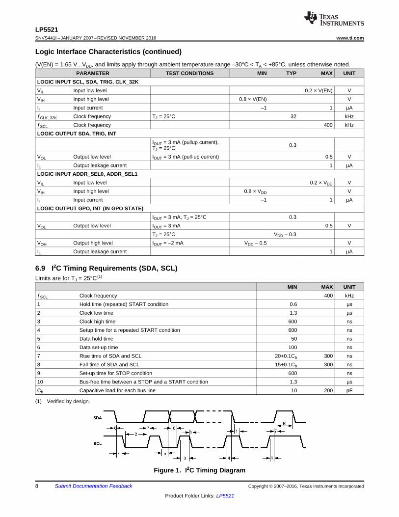
6.9 I2C Timing Requirements (SDA, SCL)Limits are for TJ = 25°C (1)
MIN MAX UNITƒSCL Clock frequency 400 kHz1 Hold time (repeated) START condition 0.6 µs2 Clock low time 1.3 µs3 Clock high time 600 ns4 Setup time for a repeated START condition 600 ns5 Data hold time 50 ns6 Data set-up time 100 ns7 Rise time of SDA and SCL 20+0.1Cb 300 ns8 Fall time of SDA and SCL 15+0.1Cb 300 ns9 Set-up time for STOP condition 600 ns10 Bus-free time between a STOP and a START condition 1.3 µsCb Capacitive load for each bus line 10 200 pF
7.1 OverviewThe LP5521 is a three-channel LED driver designed to produce variety of lighting effects for mobile devices. Ahigh-efficiency charge pump enables LED driving over full Li-Ion battery voltage range. The device has aprogram memory for creating variety of lighting sequences. When program memory has been loaded, theLP5521 can operate autonomously without processor control allowing power savings.
The device maintains excellent efficiency over a wide operating range by automatically selecting proper chargepump gain based on LED forward voltage requirements. the LP5521 is able to automatically enter power-savemode, when LED outputs are not active and thus lowering current consumption.
Three independent LED channels have accurate programmable current sources and PWM control. Each channelhas program memory for creating desired lighting sequences with PWM control.
The LP5521 has a flexible digital interface. A trigger I/O and 32-kHz clock input allow synchronization betweenmultiple devices. Interrupt output can be used to notify processor, when LED sequence has ended. LP5521 hasfour pin-selectable I2C-compatible addresses. This allows connecting up to four parallel devices in one I2C-compatible bus. GPO and INT pins can be used as a digital control pin for other devices.
The LP5521 requires only four small and low-cost ceramic capacitors.
Comprehensive application tools are available, including command compiler for easy LED sequenceprogramming.
7.3.1 Charge Pump Operational DescriptionThe LP5521 includes a pre-regulated switched-capacitor charge pump with a programmable voltagemultiplication of 1 and 1.5×.
In 1.5× mode by combining the principles of a switched-capacitor charge pump and a linear regulator, the devicegenerates a regulated 4.5-V output from Li-Ion input voltage range. A two-phase non-overlapping clockgenerated internally controls the operation of the charge pump. During the charge phase, both flying capacitors(CFLY1 and CFLY2) are charged from input voltage. In the pump phase that follows, the flying capacitors aredischarged to output. A traditional switched capacitor charge pump operating in this manner uses switches withvery low on-resistance, ideally 0 Ω, to generate an output voltage that is 1.5× the input voltage. The LP5521regulates the output voltage by controlling the resistance of the input-connected pass-transistor switches in thecharge pump.
7.3.1.1 Output ResistanceAt lower input voltages, the charge pump output voltage may degrade due to effective output resistance (ROUT) ofthe charge pump. The expected voltage drop can be calculated by using a simple model for the charge pumpshown in Figure 14.
Figure 14. Charge Pump Block Diagram
The model shows a linear pre-regulation block (REG), a voltage multiplier (1.5×), and an output resistance(ROUT). Output resistance models the output voltage drop that is inherent to switched capacitor converters. Theoutput resistance is 3.5 Ω (typical) and is function of switching frequency, input voltage, capacitance value of theflying capacitors, internal resistances of switches, and ESR of flying capacitors. When the output voltage is inregulation, the regulator in the model controls the voltage V’ to keep the output voltage equal to 4.5 V (typical).With increased output current, the voltage drop across ROUT increases. To prevent drop in output voltage, thevoltage drop across the regulator is reduced, V’ increases, and VOUT remains at 4.5 V. When the output currentincreases to the point that there is zero voltage drop across the regulator, V’ equals the input voltage, and theoutput voltage is on the edge of regulation. Additional output current causes the output voltage to fall out ofregulation, so that the operation is similar to a basic open-loop 1.5× charge pump. In this mode, output currentresults in output voltage drop proportional to the output resistance of the charge pump. The out-of-regulationoutput voltage can be approximated by: VOUT= 1.5 × VIN – IOUT × ROUT.
7.3.1.2 Controlling Charge PumpThe charge pump is controlled with two CP_MODE bits in register 08H. When both bits are low, the charge pumpis disabled, and the output voltage is pulled down with 300 kΩ. Charge pump can be forced to bypass mode, sothat battery voltage is going directly to RGB outputs. In 1.5× mode output voltage is boosted to 4.5 V. Inautomatic mode, charge pump operation mode is defined by LED outputs saturation described in LED ForwardVoltage Monitoring. Table 1 lists operation modes and selection bits.
Table 1. CONFIG Register (08H)NAME BIT DESCRIPTION
7.3.1.3 LED Forward Voltage MonitoringWhen charge pump automatic mode selection is enabled, voltages over LED drivers are monitored. If drivers donot have enough headroom, charge pump gain is set to 1.5×. Driver saturation monitor does not have a fixedvoltage limit, since saturation voltage is a function of temperature and current. Charge pump gain is set to 1×,when battery voltage is high enough to supply all LEDs.
In automatic gain change mode, charge pump is switched to bypass mode (1×), when LEDs are inactive for over50 ms.
Charge pump gain control utilizes digital filtering to prevent supply voltage disturbances from triggering gainchanges. If the R driver current source is connected to a battery (address 08H, bit R_TO_BATT = 1), voltagemonitoring is disabled in R output, but still functional in B and G outputs.
LED forward voltage monitoring and gain control block diagram is shown in Figure 15.
Figure 15. Voltage Monitoring Block Diagram for One Output
7.3.2 LED Driver Operational DescriptionThe LP5521 LED drivers are constant current sources with 8-bit PWM control. Output current can beprogrammed with I2C register up to 25.5 mA. Current setting resolution is 100 μA (8-bit control).
R driver has two modes: current source can be connected to the battery (VDD) or to the charge pump output. If acurrent source is connected to the battery, automatic charge pump gain control is not used for this output. Thisapproach provides better efficiency when LED with low VF is connected to R driver, and battery voltage is highenough to drive this LED in all conditions. R driver mode can be selected with I2C register bit. When address08H, bit R_TO_BATT = 1, R current source is connected to battery. When it is 0 (default), R current source isconnected to charge pump same way as in G and B drivers. G and B drivers are always connected to chargepump output.
Some LED configuration examples are given in Table 2. When LEDs with low VF are used, charge pump can beoperating in bypass mode (1×). This eliminates the need of having double drivers for all outputs; one connectedto battery and another connected to charge pump output. When LP5521 is driving a RGB LED, R channel can beconfigured to use battery power. This configuration increases power efficiency by minimizing the voltage dropacross the LED driver.
Table 2. LED Configuration ExamplesCONFIGURATION R OUTPUT TO BATT R OUTPUT TO CP CP MODE
RGB LED with low VF red X Auto (1× or 1.5×)3 × low VF LED X 1×3 × white LED X Auto (1× or 1.5×)
PWM frequency is either 256 Hz or 558 Hz, frequency is set with PWM_HF bit in register 08H. When PWM_HFis 0, the frequency is 256 Hz, and when bit is 1, the PWM frequency is 558 Hz. Brightness adjustment is eitherlinear or logarithmic. This can be set with register 00H LOG_EN bit. When LOG_EN = 0 linear adjustment scaleis used, and when LOG_EN = 1 logarithmic scale is used. By using logarithmic scale the visual effect seemslinear to the eye. Register control bits are presented in Table 3, Table 4, and Table 5:
Table 5. CONFIG Register (08H):NAME BIT DESCRIPTION
PWM_HF 6 PWM clock frequency0 = 256 Hz, frequency defined by the 32-kHz clock (internal or external)1 = 558 Hz, frequency defined by internal oscillator
Figure 16. Logarithmic and Linear PWM Adjustment Curves
7.3.3 Automatic Power SaveAutomatic power save mode is enabled when PWRSAVE_EN bit in register address 08H is 1. Almost all analogblocks are powered down in power save, if external clock is used. Only charge pump protection circuits remainactive. However if internal clock has been selected only charge pump and led drivers are disabled during powersave since digital part of the LED controller need to remain active. In both cases charge pump enters 'weak 1×'mode. In this mode charge pump utilizes a passive current limited keep-alive switch, which keeps the outputvoltage at battery level.
During program execution LP5521 can enter power save if there is no PWM activity in R, G and B outputs. Toprevent short power save sequences during program execution, LP5521 has command look-ahead filter. In everyinstruction cycle R, G, B commands are analyzed, and if there is sufficient time left with no PWM activity, thedevice enters power save. In power save program execution continues uninterruptedly. When a command thatrequires PWM activity is executed, fast internal start-up sequence will be started automatically. Table 6 describecommands and conditions that can activate power save. All channels (R,G,B) need to meet power save conditionin order to enable power save.
Table 6. LED Controller OperationLED CONTROLLER OPERATION
MODE (R,G,B_MODE)POWER SAVE CONDITION
00b Disabled mode enables power save01b Load program to SRAM mode prevents power save
10b Run program mode enables power save if there is no PWM activity and commandlook-ahead filter condition is met
11b Direct control mode enables power save if there is no PWM activity
COMMAND POWER SAVE CONDITION
Wait No PWM activity and current command wait time longer than 50 ms. If prescale = 1then wait time needs to be longer than 80 ms.
Ramp Ramp Command PWM value reaches minimum 0 and current command executiontime left more than 50 ms. If prescale = 1 then time left needs to be more than 80 ms.
Trigger No PWM activity during wait for trigger command execution.End No PWM activity or Reset bit = 1
Set PWM Enables power save if PWM set to 0 and next command generates at least 50 ms waitOther commands No effect to power save
See application note LP5521 Power Efficiency Considerations (SNVA185) for more information.
7.3.4 External Clock DetectionThe presence of external clock can be detected by the LP5521. Program execution is clocked with internal 32kHz clock or with external clock. Clocking is controlled with register address 08H bits, INT_CLK_EN andCLK_DET_EN as seen on the following table.
External clock can be used if clock is present at CLK_32K pin. External clock frequency must be 32 kHz for theprogram execution / PWM timing to be like specified. If higher or lower frequency is used, it will affect theprogram engine execution speed. If other than 32 kHz clock frequency is used, the program execution timingsmust be scaled accordingly. The external clock detector block only detects too low clock frequency (< 15 kHz). Ifexternal clock frequency is higher than specified, the external clock detector notifies that external clock ispresent. External clock status can be checked with read only bit EXT_CLK_USED in register address 0CH, whenthe external clock detection is enabled (CLK_DET_EN bit = high). If EXT_CLK_USED = 1, then the externalclock is detected and it is used for timing, if automatic clock selection is enabled (see Table 7).
If external clock is stuck-at-zero or stuck-at-one, or the clock frequency is too low, the clock detector indicatesthat external clock is not present.
If external clock is not used on the application, connect the CLK_32K pin to GND to prevent floating of this pinand extra current consumption.
7.3.5 Logic Interface Operational DescriptionLP5521 features a flexible logic interface for connecting to processor and peripheral devices. Communication isdone with I2C compatible interface and different logic input/output pins makes it possible to synchronizeoperation of several devices.
7.3.5.1 I/O LevelsI2C interface, CLK_32K and TRIG pins input levels are defined by EN pin. Using EN pin as voltage reference forlogic inputs simplifies PWB routing and eliminates the need for dedicated VIO pin. Figure 17 describes EN pinconnections.
Figure 17. Using EN Pin as Digital I/O Voltage Reference
ADDR_SEL0/1 are referenced to VDD voltage. GPO pin level is defined by VDD voltage.
7.3.5.2 GPO/INT PinsLP5521 has one General Purpose Output pin (GPO); the INT pin can also be configured as a GPO pin. WhenINT is configured as GPO output, its level is defined by the VDD voltage. State of the pins can be controlled withGPO register (0EH). GPO pins are digital CMOS outputs and no pullup or pulldown resistors are needed.
When INT pin GPO function is disabled, it operates as an open drain pin. INT signal is active low; that is, wheninterrupt signal is sent, the pin is pulled to GND. External pullup resistor is needed for proper functionality.
Table 8. GPO Register (0EH)NAME BIT DESCRIPTION
INT_AS_GPO 2Enable INT pin GPO function0 = INT pin functions as a INT pin1 = INT pin functions as a GPO pin
GPO 1 0 = GPO pin state is low1 = GPO pin state is high
INT 0 0 = INT pin state is low (INT_AS_GPO=1)1 = INT pin state is high (INT_AS_GPO=1)
7.3.5.3 TRIG PinThe TRIG pin can function as an external trigger input or output. External trigger signal is active low; that is,when trigger is sent or received the pin is pulled to GND. TRIG is an open-drain pin and external pullup resistoris needed for trigger line. External trigger input signal must be at least two 32-kHz clock cycles long to berecognized. Trigger output signal is three 32-kHz clock cycles long. If TRIG pin is not used on application,connected the TRIG pin to GND to prevent floating of this pin and extra current consumption.
7.3.5.4 ADDR_SEL0,1 PinsThe ADDR_SEL0,1 pins define the chip I2C address. Pins are referenced to VDD signal level. See I2C-CompatibleSerial Bus Interface for I2C address definitions.
7.3.5.5 CLK_32K PinThe CLK_32K pin is used for connecting an external 32-kHz clock to LP5521. External clock can be used tosynchronize the sequence engines of several LP5521. Using external clock can also improve automatic powersave mode efficiency, because internal clock can be switched off automatically when device has entered powersave mode, and external clock is present. See application note LP5521 Power Efficiency Considerations(SNVA185) for more information.
Device can be used without the external clock. If external clock is not used on the application, connect theCLK_32K pin to GND to prevent floating of this pin and extra current consumption.
(1) Internal thermal shutdown circuitry protects the device from permanent damage. Thermal shutdown engages at TJ = 150°C (typical) anddisengages at TJ = 130°C (typical).
7.4 Device Functional Modes
7.4.1 Modes of OperationRESET: In the RESET mode all the internal registers are reset to the default values. Reset is done always if
Reset Register (0DH) is written FFH or internal power on reset (POR) is activated. POR activateswhen supply voltage is connected or when the supply voltage VDD falls below 1.5 V typical (0.8 Vminimum). Once VDD rises above 1.5 V, POR inactivates, and the chip continues to the STANDBYmode. CHIP_EN control bit is low after POR by default.
STANDBY: The STANDBY mode is entered if the register bit CHIP_EN or EN pin is LOW and Reset is notactive. This is the low power consumption mode, when all circuit functions are disabled. Registerscan be written in this mode if EN pin is high. Control bits are effective after start-up.
START-UP: When CHIP_EN bit is written high and EN pin is high, the INTERNAL STARTUP SEQUENCEpowers up all the needed internal blocks (VREF, bias, oscillator, etc.). Start-up delay is after settingEN pin high is 1 ms (typical). Start-up delay after setting CHIP_EN to 1 is 500 μs (typical). If thechip temperature rises too high, the thermal shutdown (TSD) disables the chip operation, and thechip state is in START-UP mode until no TSD event is present. (1)
NORMAL: During NORMAL mode the user controls the chip using the Control Registers. If EN pin is set low,the CHIP_EN bit is reset to 0.
POWER SAVE: In POWER SAVE mode analog blocks are disabled to minimize power consumption. SeeAutomatic Power Save for further information.
7.5.1.1 Interface Bus OverviewThe I2C compatible synchronous serial interface provides access to the programmable functions and registers onthe device. This protocol uses a two-wire interface for bidirectional communications between the IC's connectedto the bus. The two interface lines are the serial data line (SDA), and the serial clock line (SCL). These linesshould be connected to a positive supply, via a pullup resistor and remain HIGH even when the bus is idle.
Every device on the bus is assigned a unique address and acts as either a Master or a Slave depending onwhether it generates or receives the serial clock (SCL).
7.5.1.2 Data TransactionsOne data bit is transferred during each clock pulse. Data is sampled during the high state of the serial clock(SCL). Consequently, throughout the high period of the clock the data should remain stable. Any changes on theSDA line during the high state of the SCL and in the middle of a transaction, aborts the current transaction. Newdata should be sent during the low SCL state. This protocol permits a single data line to transfer bothcommand/control information and data using the synchronous serial clock.
Figure 19. Data Validity
Each data transaction is composed of a start condition, a number of byte transfers (set by the software) and astop condition to terminate the transaction. Every byte written to the SDA bus must be 8 bits long and istransferred with the most significant bit first. After each byte, an acknowledge signal must follow. The followingsections provide further details of this process.
Figure 20. Acknowledge Signal
The Master device on the bus always generates the start and stop conditions (control codes). After a startcondition is generated, the bus is considered busy and it retains this status until a certain time after a stopcondition is generated. A high-to-low transition of the data line (SDA) while the clock (SCL) is high indicates astart condition. A low-to-high transition of the SDA line while the SCL is high indicates a stop condition.
In addition to the first start condition, a repeated start condition can be generated in the middle of a transaction.This allows another device to be accessed, or a register read cycle.
7.5.1.3 Acknowledge CycleThe acknowledge cycle consists of two signals: the acknowledge clock pulse the master sends with each bytetransferred, and the acknowledge signal sent by the receiving device.
The master generates the acknowledge clock pulse on the ninth clock pulse of the byte transfer. The transmitterreleases the SDA line (permits it to go high) to allow the receiver to send the acknowledge signal. The receivermust pull down the SDA line during the acknowledge clock pulse and ensure that SDA remains low during thehigh period of the clock pulse, thus signaling the correct reception of the last data byte and its readiness toreceive the next byte.
7.5.1.4 Acknowledge After Every Byte RuleThe master generates an acknowledge clock pulse after each byte transfer. The receiver sends an acknowledgesignal after every byte received.
There is one exception to the acknowledge after every byte rule. When the master is the receiver, it mustindicate to the transmitter an end of data by not-acknowledging (negative acknowledge) the last byte clocked outof the slave. This negative acknowledge still includes the acknowledge clock pulse (generated by the master),but the SDA line is not pulled down.
7.5.1.5 Addressing Transfer FormatsEach device on the bus has a unique slave address. The LP5521 operates as a slave device with the 7-bitaddress. The LP5521 I2C address is pin selectable from four different choices. If 8-bit address is used forprogramming, the 8th bit is 1 for read and 0 for write. Table 9 shows the 8-bit I2C addresses.
Before any data is transmitted, the master transmits the address of the slave being addressed. The slave devicesends an acknowledge signal on the SDA line, once it recognizes its address.
The slave address is the first seven bits after a start condition. The direction of the data transfer (R/W) dependson the bit sent after the slave address — the eighth bit.
When the slave address is sent, each device in the system compares this slave address with its own. If there is amatch, the device considers itself addressed and sends an acknowledge signal. Depending upon the state of theR/W bit (1:read, 0:write), the device acts as a transmitter or a receiver.
7.5.1.6 Control Register Write Cycle• Master device generates start condition.• Master device sends slave address (7 bits) and the data direction bit (r/w = 0).• Slave device sends acknowledge signal if the slave address is correct.• Master sends control register address (8 bits).• Slave sends acknowledge signal.• Master sends data byte to be written to the addressed register.• Slave sends acknowledge signal.• If master will send further data bytes the control register address is incremented by one after acknowledge
signal.• Write cycle ends when the master creates stop condition.
7.5.1.7 Control Register Read Cycle• Master device generates a start condition.• Master device sends slave address (7 bits) and the data direction bit (r/w = 0).• Slave device sends acknowledge signal if the slave address is correct.• Master sends control register address (8 bits).• Slave sends acknowledge signal.• Master device generates repeated start condition.• Master sends the slave address (7 bits) and the data direction bit (r/w = 1).• Slave sends acknowledge signal if the slave address is correct.• Slave sends data byte from addressed register.• If the master device sends acknowledge signal, the control register address is incremented by one. Slave
device sends data byte from addressed register.• Read cycle ends when the master does not generate acknowledge signal after data byte and generates stop
When a READ function is to be accomplished, a WRITE function must precede the READ function, as shown inFigure 24.
w = write (SDA = 0)r = read (SDA = 1)ack = acknowledge (SDA pulled down by either master or slavers = repeated startid = 7-bit chip address
Figure 24. Register Read Format
7.5.2 LED Controller Operation Modes
Operation modes are defined in register address 01H. Each output channel (R, G, B) operation mode can beconfigured separately. MODE registers are synchronized to a 32-kHz clock. Delay between consecutive I2Cwrites to OP_MODE register (01H) need to be longer than 153 µs (typical).
Table 10. OP_MODE Register (01H):NAME BIT DESCRIPTION
R_MODE 5:4 R channel operation mode00b = Disabled, reset R channel PC01b = Load program to SRAM, reset R channel PC10b = Run program defined by R_EXEC11b = Direct control, reset R channel PC
G_MODE 3:2 G channel operation mode00b = Disabled, reset G channel PC01b = Load program to SRAM, reset G channel PC10b = Run program defined by G_EXEC11b = Direct control, reset G channel PC
B_MODE 1:0 B channel operation mode00b = Disabled, reset B channel PC01b = Load program to SRAM, reset B channel PC10b = Run program defined by B_EXEC11b = Direct control, reset B channel PC
7.5.2.1 DisabledEach channel can be configured to disabled mode. LED output current is 0 during this mode. Disabled moderesets PC of respective channel.
7.5.2.2 LOAD ProgramLP5521 can store 16 commands for each channel (R, G, B). Each command consists of 16 bits. Because oneregister has only 8 bits, one command requires two I2C register addresses. In order to reduce program load timeLP5521 supports address auto incrementation. Register address is incremented after each 8 data bits. Wholeprogram memory can be written in one I2C write sequence.
Program memory is defined in the LP5521 register table, 10H to 2FH for R channel, 30H to 4FH for G channeland 50H to 6FH for B channel. In order to be able to access program memory at least one channel operationmode needs to be LOAD Program.
Memory writes are allowed only to the channel in LOAD mode. All channels are in hold while one or severalchannels are in LOAD program mode, and PWM values are frozen for the channels which are not in LOADmode. Program execution continues when all channels are out of LOAD program mode. LOAD Program moderesets PC of respective channel.
7.5.2.3 RUN ProgramRUN Program mode executes the commands defined in program memory for respective channel (R, G, B).Execution register bits in ENABLE register define how program is executed. Program start position can beprogrammed to Program Counter register (see the following tables). By manually selecting the PC start value,user can write different lighting sequences to the memory, and select appropriate sequence with the PC register.If program counter runs to end (15) the next command will be executed from program location 0.
If internal clock is used in the RUN program mode, operation mode needs to be written disabled (00b) beforedisabling the chip (with CHIP_EN bit or EN pin) to ensure that the sequence starts from the correct programcounter (PC) value when restarting the sequence.
PC registers are synchronized to 32 kHz clock. Delay between consecutive I2C writes to PC registers (09H, 0AH,0BH) need to be longer than 153 µs (typ.).
Note that entering LOAD program or Direct Control Mode from RUN PROGRAM mode is not allowed. Engineexecution mode should be set to Hold, and Operation Mode to disabled, when changing operation mode fromRUN mode.
Table 11. R Channel PC Register (09H), G CHANNEL PC Register (0AH), B CHANNEL PC Register (0BH)NAME BIT DESCRIPTION
PC 3:0 Program counter value from 0 to 15d
Table 12. ENABLE Register (00H)NAME BIT DESCRIPTION
R_EXEC 5:4 R channel program execution00b = Hold: Wait until current command is finished then stop while EXEC mode is hold. PC can be reador written only in this mode.01b = Step: Execute instruction defined by current R channel PC value, increment PC and changeR_EXEC to 00b (Hold)10b = Run: Start at program counter value defined by current R channel PC value11b = Execute instruction defined by current R channel PC value and change R_EXEC to 00b (Hold)
G_EXEC 3:2 G channel program execution00b = Hold: Wait until current command is finished then stop while EXEC mode is hold. PC can be reador written only in this mode.01b = Step: Execute instruction defined by current G channel PC value, increment PC and changeG_EXEC to 00b (Hold)10b = Run: Start at program counter value defined by current G channel PC value11b = Execute instruction defined by current G channel PC value and change G_EXEC to 00b (Hold)
Table 12. ENABLE Register (00H) (continued)NAME BIT DESCRIPTION
B_EXEC 1:0 B channel program execution00b = Hold: Wait until current command is finished then stop while EXEC mode is hold. PC can be reador written only in this mode.01b = Step: Execute instruction defined by current B channel PC value, increment PC and changeB_EXEC to 00b (Hold)10b = Run: Start at program counter value defined by current B channel PC value11b = Execute instruction defined by current B channel PC value and change B_EXEC to 00b (Hold)
EXEC registers are synchronized to 32-kHz clock. Delay between consecutive I2C writes to ENABLE register(00H) need to be longer than 488 μs (typ.).
7.5.2.3.1 DIRECT Control
When R, G or B channel mode is set to 11b, the LP5521 drivers work in direct control mode. LP5521 LEDchannels can be controlled independently through I2C. For each channel there is a PWM control register and aoutput current control register. With output current control register is set what is the maximum output current with8-bit resolution, step size is 100 μA. Duty cycle can be set with 8-bit resolution. Direct control mode resetsrespective channel’s PC. PWM control bits are presented in Table 13:
Table 13. R_PWM Register (02H), G_PWM Register (03H), B_PWM Register (04H):NAME BIT DESCRIPTIONPWM 7:0 LED PWM value during direct control operation mode
0000 0000b = 0%1111 1111b = 100%
If charge pump automatic gain change is used in this mode, then PWM values need to be written 0 beforechanging the drivers’ operation mode to disabled (00b) to ensure proper automatic gain change operation.
7.5.3 LED Controller Programming CommandsLP5521 has three independent programmable channels (R, G, B). Trigger connections between channels arecommon for all channels. All channels have own program memories for storing complex patterns. Brightnesscontrol and patterns are done with 8-bit PWM control (256 steps) to get accurate and smooth color control.
Program execution is timed with 32 768 Hz clock. This clock can be generated internally or external 32 kHz clockcan be connected to CLK_32K pin. Using external clock enables synchronization of LED timing to this clockrather than internal clock. Selection of the clock is made with address 08H bits INT_CLK_EN and CLK_DET_EN.See External Clock Detection for details.
Supported commands are listed in Table 14. Command compiler is available for easy sequenceprogramming. With Command compiler it is possible to write sequences with simple ASCII commands,which are then converted to binary or hex format. See application note "LP5521 ProgrammingConsiderations" for examples of Command compiler usage.
7.5.3.1 RAMP/WAITRamp command generates a PWM ramp starting from current value. At each ramp step the output isincremented by one. Time for one step is defined with Prescale and Step time bits. Minimum time for one step is0.49 ms and maximum time is 63 × 15.6 ms = 1 second/step, so it is possible to program very fast and also veryslow ramps. Increment value defines how many steps are taken in one command. Number of actual steps isIncrement + 1. Maximum value is 127d, which corresponds to half of full scale (128 steps). If during rampcommand PWM reaches minimum/maximum (0/255) ramp command is executed to the end, and PWM stays atminimum/maximum. This enables ramp command to be used as combined ramp and wait command in a singleinstruction.
Ramp command can be used as wait instruction when increment is zero.
Setting register 00H bit LOG_EN sets the scale from linear to logarithmic. When LOG_EN = 0 linear scale isused, and when LOG_EN = 1 logarithmic scale is used. By using logarithmic scale the visual effect of the rampcommand seems linear to the eye.
Prescale0 Divides master clock (32 768Hz) by 16 = 2048 Hz, 0.49 ms cycle time1 Divides master clock (32 768Hz) by 512 = 64 Hz, 15.6 ms cycle time
Step time 1-63 One ramp increment done in (step time) x (clock after prescale) Note: 0 means SetPMW command.
Sign0 Increase PWM output1 Decrease PWM output
Increment 0-127 The number of steps is Increment + 1. Note: 0 is a wait instruction.
Application example:For example if following parameters are used for ramp:• Prescale = 1 → cycle time = 15.6 ms• Step time = 2 → time = 15.6 ms x 2 = 31.2 ms• Sign = 0 → rising ramp• Increment = 4 → 5 cycles
Ramp command will be: 0100 0010 0000 0100b = 4204H
If current PWM value is 3, and the first command is as described above and next command is a ramp withotherwise same parameters, but with Sign = 1 (Command = 4284H), the result will be like in Figure 25:
7.5.3.2 Set PWMSet PWM output value from 0 to 255. Command takes sixteen 32 kHz clock cycles (= 488 μs). Setting register00H bit LOG_EN sets the scale from linear to logarithmic.
7.5.3.3 Go to StartGo to start command resets Program Counter register and continues executing program from the 00H location.Command takes sixteen 32 kHz clock cycles. Note that default value for all program memory registers is 0000H,which is Go to start command.
7.5.3.4 BranchWhen branch command is executed, the 'step number' value is loaded to PC and program execution continuesfrom this location. Looping is done by the number defined in loop count parameter. Nested looping is supported(loop inside loop). The number of nested loops is not limited. Command takes sixteen 32-kHz clock cycles.
Table 17. Branch Command15 14 13 12 11 10 9 8 7 6 5 4 3 2 1 01 0 1 Loop count X X X Step number
NAME VALUE(d) DESCRIPTIONloop count 0-63 The number of loops to be done. 0 means infinite loop.
step number 0-15 The step number to be loaded to program counter.
7.5.3.5 EndEnd program execution, resets the program counter and sets the corresponding EXEC register to 00b (hold).Command takes sixteen 32-kHz clock cycles.
Table 18. End Command15 14 13 12 11 10 9 8 7 6 5 4 3 2 1 01 1 0 int reset X X X X X X X X X X X
NAME VALUE DESCRIPTION
int
0 No interrupt will be sent.
1Send interrupt to processor by pulling the INT pin down and setting corresponding statusregister bit high to notify that program has ended. Interrupt can only be cleared by readinginterrupt status register 0CH.
reset0 Keep the current PWM value.1 Set PWM value to 0.
7.5.3.6 TriggerWait or send triggers can be used to, for example, synchronize operation between different channels. Sendtrigger command takes sixteen 32-kHz clock cycles, and wait for trigger takes at least sixteen 32 kHz clockcycles. The receiving channel stores sent triggers. Received triggers are cleared by wait for trigger command ifreceived triggers match to channels defined in the command. Channel waits for until all defined triggers havebeen received.
External trigger input signal must be at least two 32-kHz clock cycles (= 61 μs typical) long to be recognized.Trigger output signal is three 32-kHz clock cycles (92 μs typical) long. External trigger signal is active low; that is,when trigger is sent/received the pin is pulled to GND. Sent external trigger is masked; that is, the device whichhas sent the trigger does not recognize it. If send and wait external trigger are used on the same command, thesend external trigger is executed first, then the wait external trigger.
wait trigger<5:0> 0-31Wait for trigger for the channel(s) defined. Several triggers can be defined in the samecommand. Bit 0 is R, bit 1 is G, bit 2 is B and bit 5 is external trigger I/O. Bits 3 and 4are not in use.
send trigger<5:0> 0-31Send trigger for the channel(s) defined. Several triggers can be defined in the samecommand. Bit 0 is R, bit 1 is G, bit 2 is B and bit 5 is external trigger I/O. Bits 3 and 4are not in use.
Table 20. LP5521 Control Register Names and Default ValuesADDR(HEX) REGISTER D7 D6 D5 D4 D3 D2 D1 D0 DEFAULT
00 ENABLE LOG_EN CHIP_EN R_EXEC[1:0] G_EXEC[1:0] B_EXEC[1:0] 0000 000001 OP MODE R_MODE[1:0] G_MODE[1:0] B_MODE[1:0] 0000 000002 R PWM R_PWM[7:0] 0000 000003 G PWM G_PWM[7:0] 0000 000004 B PWM B_PWM[7:0] 0000 000005 R CURRENT R_CURRENT[7:0] 1010 111106 G CURRENT G_CURRENT[7:0] 1010 111107 B CURRENT B_CURRENT[7:0] 1010 111108 CONFIG PWM_HF PWRSAVE_EN CP_MODE[1:0] R_TO_BATT CLK_DET_EN INT_CLK_EN 0000 000009 R PC R_PC[3:0] 0000 00000A G PC G_PC[3:0] 0000 00000B B PC B_PC[3:0] 0000 00000C STATUS EXT_CLK_USED R_INT G_INT B_INT 0000 00000D RESET RESET[7:0] 0000 00000E GPO INT_AS_GPO GPO INT 0000 000010 PROG MEM R CMD_R1[15:8] 0000 000011 PROG MEM R CMD_R1[7:0] 0000 0000
...2E PROG MEM R CMD_R16[15:8] 0000 00002F PROG MEM R CMD_R16[7:0] 0000 000030 PROG MEM G CMD_G1[15:8] 0000 000031 PROG MEM G CMD_G1[7:0] 0000 0000
...4E PROG MEM G CMD_G16[15:8] 0000 00004F PROG MEM G CMD_G16[7:0] 0000 000050 PROG MEM B CMD_B1[15:8] 0000 000051 PROG MEM B CMD_B1[7:0] 0000 0000
...6E PROG MEM B CMD_B16[15:8] 0000 00006F PROG MEM B CMD_B16[7:0] 0000 0000
NAME BIT ACCESS ACTIVE DESCRIPTIONLOG_EN 7 R/W High Logarithmic PWM adjustment generation enable
CHIP_EN 6 R/W HighMaster chip enable. Enables device internal startup sequence. Startup delayafter setting CHIP_EN is 500 μs. See Operation for further information.Setting EN pin low resets the CHIP_EN state to 0.
R_EXEC 5:4 R/W
R channel program execution.00b = Hold: Wait until current command is finished then stop while EXECmode is hold. PC can be read or written only in this mode.01b = Step: Execute instruction defined by current R channel PC value,increment PC and change R_EXEC to 00b (Hold)10b = Run: Start at program counter value defined by current R Channel PCvalue11b = Execute instruction defined by current R channel PC value and changeR_EXEC to 00b (Hold)
G_EXEC 3:2 R/W
G channel program execution00b = Hold: Wait until current command is finished then stop while EXECmode is hold. PC can be read or written only in this mode.01b = Step: Execute instruction defined by current G channel PC value,increment PC and change G_EXEC to 00b (Hold)10b = Run: Start at program counter value defined by current G Channel PCvalue11b = Execute instruction defined by current G channel PC value andchange G_EXEC to 00b (Hold)
B_EXEC 1:0 R/W
B channel program execution00b = Hold: Wait until current command is finished then stop while EXECmode is hold. PC can be read or written only in this mode.01b = Step: Execute instruction defined by current B channel PC value,increment PC and change B_EXEC to 00b (Hold)10b = Run: Start at program counter value defined by current B Channel PCvalue11b = Execute instruction defined by current B channel PC value and changeB_EXEC to 00b (Hold)
EXEC registers are synchronized to 32 kHz clock. Delay between consecutive I2C writes to ENABLE register(00H) need to be longer than 488 μs (typ).
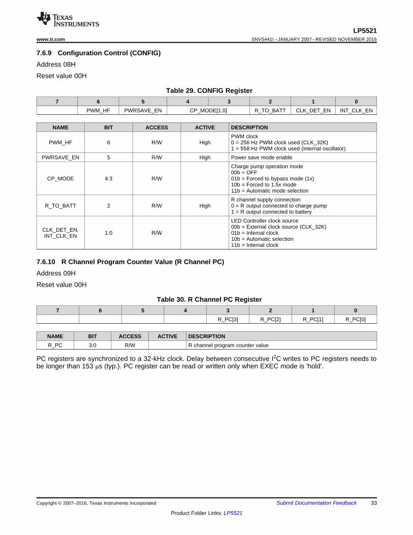
7.6.10 R Channel Program Counter Value (R Channel PC)Address 09H
Reset value 00H
Table 30. R Channel PC Register7 6 5 4 3 2 1 0
R_PC[3] R_PC[2] R_PC[1] R_PC[0]
NAME BIT ACCESS ACTIVE DESCRIPTIONR_PC 3:0 R/W R channel program counter value
PC registers are synchronized to a 32-kHz clock. Delay between consecutive I2C writes to PC registers needs tobe longer than 153 μs (typ.). PC register can be read or written only when EXEC mode is 'hold'.
7.6.11 G Channel Program Counter Value (G Channel PC)Address 0AH
Reset value 00H
Table 31. G Channel PC Register7 6 5 4 3 2 1 0
G_PC[3] G_PC[2] G_PC[1] G_PC[0]
NAME BIT ACCESS ACTIVE DESCRIPTIONG_PC 3:0 R/W G channel program counter value
PC registers are synchronized to 32 kHz clock. Delay between consecutive I2C writes to PC registers needs tobe longer than 153 μs (typ.). PC register can be read or written only when EXEC mode is 'hold'.
7.6.12 B Channel Program Counter Value (B Channel PC)Address 0BH
Reset value 00H
Table 32. B Channel PC Register7 6 5 4 3 2 1 0
B_PC[3] B_PC[2] B_PC[1] B_PC[0]
NAME BIT ACCESS ACTIVE DESCRIPTIONB_PC 3:0 R/W B channel program counter value
PC registers are synchronized to a 32-kHz clock. Delay between consecutive I2C writes to PC registers must belonger than 153 μs (typ.). PC register can be read or written only when EXEC mode is 'hold'.
USED 3 RExternal clock state0 = Internal 32kHz clock used1 = External 32kHz clock used
R_INT 2 R High Interrupt from R channelG_INT 1 R High Interrupt from G channelB_INT 0 R High Interrupt from B channel
Note: Register INT bits will be cleared when read operation to Status/Interrupt register occurs. INT output pin(active low) will go high after read operation.
NOTEInformation in the following applications sections is not part of the TI componentspecification, and TI does not warrant its accuracy or completeness. TI’s customers areresponsible for determining suitability of components for their purposes. Customers shouldvalidate and test their design implementation to confirm system functionality.
8.1 Application InformationThe LP5521 is designed as a autonomous lighting controller for mobile devices. These devices need extremelysmall form factor; therefore, the LP5521 is designed to require only 4 small capacitors: input, output, and two fly-capacitors for charge pump. If charge pump is not needed in the application (input voltage is high enough fordriving LEDs), the charge pump capacitors can be omitted thus reducing the solution size even further. LED canbe RGB LED or any color if desired.
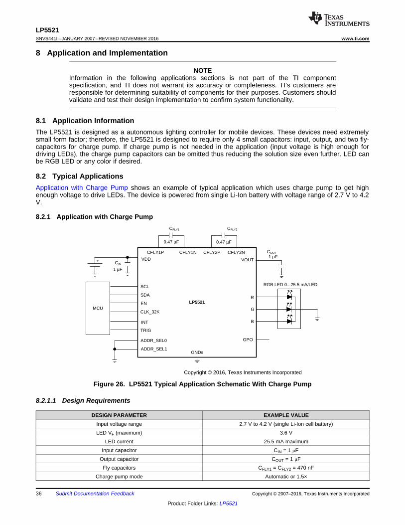
8.2 Typical ApplicationsApplication with Charge Pump shows an example of typical application which uses charge pump to get highenough voltage to drive LEDs. The device is powered from single Li-Ion battery with voltage range of 2.7 V to 4.2V.
8.2.1 Application with Charge Pump
Figure 26. LP5521 Typical Application Schematic With Charge Pump
8.2.1.1 Design Requirements
DESIGN PARAMETER EXAMPLE VALUEInput voltage range 2.7 V to 4.2 V (single Li-Ion cell battery)LED VF (maximum) 3.6 V
LED current 25.5 mA maximumInput capacitor CIN = 1 μF
The LP5521 requires 4 external capacitors for proper operation (CIN = COUT = 1 μF, CFLY1 = CFLY2 = 470 nF).Surface-mount multi-layer ceramic capacitors are recommended. These capacitors are small, inexpensive andhave very low equivalent series resistance (ESR < 20 mΩ typical). Tantalum capacitors, OS-CON capacitors,and aluminum electrolytic capacitors are not recommended for use with the LP5521 due to their high ESR, ascompared to ceramic capacitors.
For most applications, ceramic capacitors with X7R or X5R temperature characteristic are preferred for use withthe LP5521. These capacitors have tight capacitance tolerance (as good as ±10%) and hold their value overtemperature (X7R: ±15% over –55°C to 125°C; X5R: ±15% over –55°C to 85°C).
Capacitors with Y5V or Z5U temperature characteristic are generally not recommended for use with the LP5521.Capacitors with these temperature characteristics typically have wide capacitance tolerance (+80%, –20%) andvary significantly over temperature (Y5V: +22%, –82% over –30°C to +85°C range; Z5U: +22%, –56% over+10°C to +85°C range). Under some conditions, a nominal 1-μF Y5V or Z5U capacitor could have a capacitanceof only 0.1 μF. Such detrimental deviation is likely to cause Y5V and Z5U capacitors to fail to meet the minimumcapacitance requirements of the LP5521.
The minimum voltage rating acceptable for all capacitors is 6.3 V. The recommended voltage rating of the outputcapacitor is 10 V to account for DC bias capacitance losses.
NOTESome ceramic capacitors, especially those in small packages, exhibit a strong capacitancereduction with the increased applied voltage (DC bias effect). The capacitance value canfall below half of the nominal capacitance. Choose output and input capacitor with DC biasvoltage effect better than –50% at 5 V voltage (0.5 μF at 5 V).
Table 36. External Component ExamplesMODEL TYPE VENDOR VOLTAGE RATING SIZE INCH (mm)
1 μF for COUT and CIN
C1005X5R1A105K Ceramic X5R TDK 10 V 0402 (1005)ECJ0EB1A105M Ceramic X5R Panasonic 10 V 0402 (1005)ECJUVBPA105M Ceramic X5R, array of two Panasonic 10 V 0504
470 nF for CFLY1-2
C1005X5R1A474K Ceramic X5R TDK 10 V 0402 (1005)ECJ0EB0J474K Ceramic X5R Panasonic 10 V 0402 (1005)
Figure 27. Charge Pump Load Transient Response in 1.5×Mode (0 to 25.5 mA)
Figure 28. Charge Pump Line Transient Response1.5× Mode (VIN 3.5V to 4 V)
8.2.2 Application Without Charge PumpIn this application example the input voltage is high enough to drive the LEDs even without charge pump. In thatcase the charge pump components are omitted, allowing savings on bill-of-material and also board space.Charge pump must be set to 1× mode (bypass) in this case.
Figure 29. Typical Application Schematic Without Charge Pump
8.2.2.1 Design Requirements
DESIGN PARAMETER EXAMPLE VALUEInput voltage range 4.5 V to 5.5 V
8.2.2.2 Detailed Design ProceduresSelecting input and output capacitors follows the same procedure as in the application with charge pump.
8.3 Initialization Setup
8.3.1 Program Load and Execution Example1. Startup Device and Configure Device to SRAM Write Mode:
– Supply e.g. 3.6 V to VDD– Supply e.g. 1.8 V to EN– Wait 1 ms (startup delay)– Generate 32 kHz clock to CLK_32K pin– Write to address 00H 0100 0000b (enable LP5521)– Wait 500 μs (startup delay)– Write to address 01H 0001 0000b (Configure R channel into "Load program to SRAM" mode)
2. Program Load to SRAM (see Figure 30):– Write to address 10H 0000 0011b (1st ramp command 8 MSB)– Write to address 11H 0111 1111b (1st ramp command 8 LSB)– Write to address 12H 0100 1101b (1st wait command 8 MSB)– Write to address 13H 0000 0000b (1st wait command 8 LSB)– Write to address 14H 0000 0011b (2nd ramp command 8 MSB)– Write to address 15H 1111 1111b (2nd ramp command 8 LSB)– Write to address 16H 0110 0000b (2nd wait command 8 MSB)– Write to address 17H 0000 0000b (2nd wait command 8 LSB)
3. Enable Powersave, charge pump automatic mode (1x / 1.5x) and use external 32 kHz clock:– Write to address 08H 0011 1000b
4. Run program:– Write to address 01H 0010 0000b (Configure LED controller operation mode to "Run program" in R
channel– Write to address 00H 0110 0000b (Configure program execution mode from "Hold" to "Run" in R channel
LP5521 will generate 1100 ms long LED pattern which will be repeated infinitely. LED pattern is illustrated inFigure 30.
Figure 30. Sequence Diagram
8.3.2 Direct PWM Control Example1. Start up device:
– Supply, for example, 3.6 V to VDD– Supply, for example,1.8 V to EN– Wait 1 ms (start-up delay)– Write to address 00H 0100 0000b (enable LP5521)
LEDs are turned on after the PWM values are written. Changes to the PWM value registers are reflectedimmediately to the LED brightness. Default LED current (17.5 mA) is used for LED outputs, if no other values arewritten.
9 Power Supply RecommendationsThe device is designed to operate from an input voltage supply range between 2.7 V and 5.5V. In a typicalapplication this is from single Li-ion battery cell. This input supply must be well regulated and able to withstandmaximum input current and maintain stable voltage without voltage drop even at load transition condition (start-up or rapid brightness change). The resistance of the input supply rail must be low enough that the input currenttransient does not cause drop below a 2.7-V level in the LP5521 supply voltage.
10 Layout
10.1 Layout GuidelinesPlace capacitors as close to the LP5521 device as possible to minimize the current loops. Figure 31 shows anexample of LP5521 PCB layout and component placement.
11.1.1 Third-Party Products DisclaimerTI'S PUBLICATION OF INFORMATION REGARDING THIRD-PARTY PRODUCTS OR SERVICES DOES NOTCONSTITUTE AN ENDORSEMENT REGARDING THE SUITABILITY OF SUCH PRODUCTS OR SERVICESOR A WARRANTY, REPRESENTATION OR ENDORSEMENT OF SUCH PRODUCTS OR SERVICES, EITHERALONE OR IN COMBINATION WITH ANY TI PRODUCT OR SERVICE.
11.2 Documentation Support
11.2.1 Related Documentation• See LP5521 Programming Considerations for more information about programming of the device.• See LP5521 Power Efficiency Consideration for more information about powering the device and partitioning
the system.• See LP5521TM Evaluation Kit for more information about evaluation kit for LP5521TM.
11.3 Receiving Notification of Documentation UpdatesTo receive notification of documentation updates, navigate to the device product folder on ti.com. In the upperright corner, click on Alert me to register and receive a weekly digest of any product information that haschanged. For change details, review the revision history included in any revised document.
11.4 Community ResourcesThe following links connect to TI community resources. Linked contents are provided "AS IS" by the respectivecontributors. They do not constitute TI specifications and do not necessarily reflect TI's views; see TI's Terms ofUse.
TI E2E™ Online Community TI's Engineer-to-Engineer (E2E) Community. Created to foster collaborationamong engineers. At e2e.ti.com, you can ask questions, share knowledge, explore ideas and helpsolve problems with fellow engineers.
Design Support TI's Design Support Quickly find helpful E2E forums along with design support tools andcontact information for technical support.
11.5 TrademarksE2E is a trademark of Texas Instruments.All other trademarks are the property of their respective owners.
11.6 Electrostatic Discharge CautionThese devices have limited built-in ESD protection. The leads should be shorted together or the device placed in conductive foamduring storage or handling to prevent electrostatic damage to the MOS gates.
11.7 GlossarySLYZ022 — TI Glossary.
This glossary lists and explains terms, acronyms, and definitions.
12 Mechanical, Packaging, and Orderable InformationThe following pages include mechanical, packaging, and orderable information. This information is the mostcurrent data available for the designated devices. This data is subject to change without notice and revision ofthis document. For browser-based versions of this data sheet, refer to the left-hand navigation.
LP5521TM/NOPB ACTIVE DSBGA YFQ 20 250 Green (RoHS& no Sb/Br)
SNAGCU Level-1-260C-UNLIM -30 to 85 5521
LP5521TMX/NOPB ACTIVE DSBGA YFQ 20 3000 Green (RoHS& no Sb/Br)
SNAGCU Level-1-260C-UNLIM -30 to 85 5521
LP5521YQ/NOPB ACTIVE WQFN NJA 24 1000 Green (RoHS& no Sb/Br)
CU SNAGCU Level-1-260C-UNLIM -30 to 85 L5521YQ
LP5521YQX/NOPB ACTIVE WQFN NJA 24 4500 Green (RoHS& no Sb/Br)
CU SNAGCU Level-1-260C-UNLIM -30 to 85 L5521YQ
(1) The marketing status values are defined as follows:ACTIVE: Product device recommended for new designs.LIFEBUY: TI has announced that the device will be discontinued, and a lifetime-buy period is in effect.NRND: Not recommended for new designs. Device is in production to support existing customers, but TI does not recommend using this part in a new design.PREVIEW: Device has been announced but is not in production. Samples may or may not be available.OBSOLETE: TI has discontinued the production of the device.
(2) Eco Plan - The planned eco-friendly classification: Pb-Free (RoHS), Pb-Free (RoHS Exempt), or Green (RoHS & no Sb/Br) - please check http://www.ti.com/productcontent for the latest availabilityinformation and additional product content details.TBD: The Pb-Free/Green conversion plan has not been defined.Pb-Free (RoHS): TI's terms "Lead-Free" or "Pb-Free" mean semiconductor products that are compatible with the current RoHS requirements for all 6 substances, including the requirement thatlead not exceed 0.1% by weight in homogeneous materials. Where designed to be soldered at high temperatures, TI Pb-Free products are suitable for use in specified lead-free processes.Pb-Free (RoHS Exempt): This component has a RoHS exemption for either 1) lead-based flip-chip solder bumps used between the die and package, or 2) lead-based die adhesive used betweenthe die and leadframe. The component is otherwise considered Pb-Free (RoHS compatible) as defined above.Green (RoHS & no Sb/Br): TI defines "Green" to mean Pb-Free (RoHS compatible), and free of Bromine (Br) and Antimony (Sb) based flame retardants (Br or Sb do not exceed 0.1% by weightin homogeneous material)
(3) MSL, Peak Temp. - The Moisture Sensitivity Level rating according to the JEDEC industry standard classifications, and peak solder temperature.
(4) There may be additional marking, which relates to the logo, the lot trace code information, or the environmental category on the device.
(5) Multiple Device Markings will be inside parentheses. Only one Device Marking contained in parentheses and separated by a "~" will appear on a device. If a line is indented then it is a continuationof the previous line and the two combined represent the entire Device Marking for that device.
(6) Lead/Ball Finish - Orderable Devices may have multiple material finish options. Finish options are separated by a vertical ruled line. Lead/Ball Finish values may wrap to two lines if the finishvalue exceeds the maximum column width.
Important Information and Disclaimer:The information provided on this page represents TI's knowledge and belief as of the date that it is provided. TI bases its knowledge and belief on informationprovided by third parties, and makes no representation or warranty as to the accuracy of such information. Efforts are underway to better integrate information from third parties. TI has taken andcontinues to take reasonable steps to provide representative and accurate information but may not have conducted destructive testing or chemical analysis on incoming materials and chemicals.TI and TI suppliers consider certain information to be proprietary, and thus CAS numbers and other limited information may not be available for release.
In no event shall TI's liability arising out of such information exceed the total purchase price of the TI part(s) at issue in this document sold by TI to Customer on an annual basis.
A. All linear dimensions are in millimeters. Dimensioning and tolerancing per ASME Y14.5M-1994.B. This drawing is subject to change without notice.
NOTES:
4215083/A 12/12
D: Max =
E: Max =
2.093 mm, Min =
1.733 mm, Min =
2.033 mm
1.672 mm
www.ti.com
PACKAGE OUTLINE
C
24X 0.30.2
2.4 0.1
24X 0.50.3
0.8 MAXNOTE 4
SOLDER BUMP
0.1100.035
20X 0.5
2X3
2X 2
3.4 0.1
B 4.13.9
A
5.14.9
(0.2) TYP
WQFN - 0.8 mm max heightNJA0024APLASTIC QUAD FLATPACK - NO LEAD
4215212/A 04/2017
PIN 1 INDEX AREA
0.08 C
SEATING PLANE
1
713
19
8 12
24 20
(OPTIONAL)PIN 1 ID 0.1 C A B
0.05
EXPOSEDTHERMAL PAD
25
SYMM
SYMM
NOTES: 1. All linear dimensions are in millimeters. Any dimensions in parenthesis are for reference only. Dimensioning and tolerancing per ASME Y14.5M. 2. This drawing is subject to change without notice. 3. The package thermal pad must be soldered to the printed circuit board for optimal thermal and mechanical performance.4. Package maximum height does not include the solder bump height.
SCALE 2.800
www.ti.com
EXAMPLE BOARD LAYOUT
0.07 MINALL AROUND
0.07 MAXALL AROUND
24X (0.4)
24X (0.25)
( 0.2) TYPVIA
20X (0.5)
(4.4)
(3.4)
3X(1.18)
(2.4)
(R0.05) TYP
(3.4)
2X(0.86)
(0.95) TYP
WQFN - 0.8 mm max heightNJA0024APLASTIC QUAD FLATPACK - NO LEAD
4215212/A 04/2017
SYMM
1
7
8 12
13
19
2024
SYMM
LAND PATTERN EXAMPLEEXPOSED METAL SHOWN
SCALE:18X
25
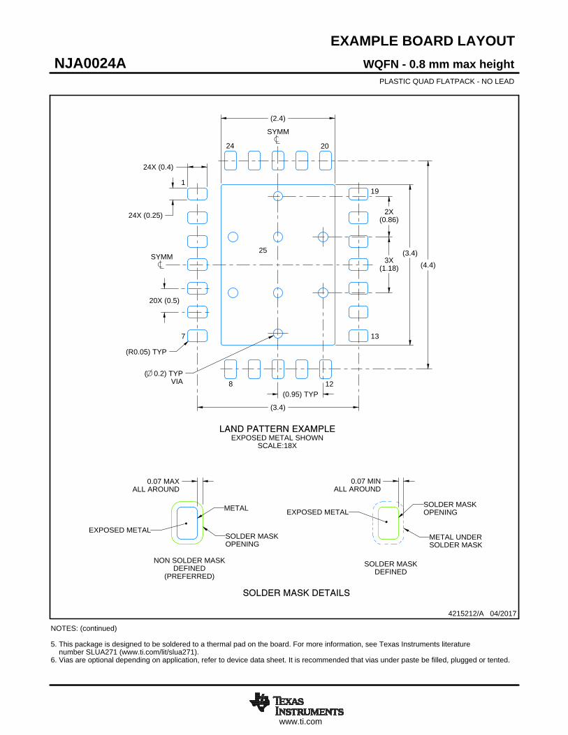
NOTES: (continued) 5. This package is designed to be soldered to a thermal pad on the board. For more information, see Texas Instruments literature number SLUA271 (www.ti.com/lit/slua271).6. Vias are optional depending on application, refer to device data sheet. It is recommended that vias under paste be filled, plugged or tented.
SOLDER MASKOPENING
METAL UNDERSOLDER MASK
SOLDER MASKDEFINED
EXPOSED METALMETAL
SOLDER MASKOPENING
SOLDER MASK DETAILS
NON SOLDER MASKDEFINED
(PREFERRED)
EXPOSED METAL
www.ti.com
EXAMPLE STENCIL DESIGN
24X (0.25)
24X (0.4)
20X (0.5)
(3.4)
(4.4)
6X (1.06)
(R0.05) TYP
6X(0.98)
(0.63) TYP
(1.18)TYP
WQFN - 0.8 mm max heightNJA0024APLASTIC QUAD FLATPACK - NO LEAD
4215212/A 04/2017
NOTES: (continued) 7. Laser cutting apertures with trapezoidal walls and rounded corners may offer better paste release. IPC-7525 may have alternate design recommendations.
SYMM
METALTYP
SOLDER PASTE EXAMPLEBASED ON 0.1 mm THICK STENCIL
EXPOSED PAD 25:
76% PRINTED SOLDER COVERAGE BY AREA UNDER PACKAGESCALE:25X
SYMM
1
7
8 12
13
19
2024
25
IMPORTANT NOTICE
Texas Instruments Incorporated (TI) reserves the right to make corrections, enhancements, improvements and other changes to itssemiconductor products and services per JESD46, latest issue, and to discontinue any product or service per JESD48, latest issue. Buyersshould obtain the latest relevant information before placing orders and should verify that such information is current and complete.TI’s published terms of sale for semiconductor products (http://www.ti.com/sc/docs/stdterms.htm) apply to the sale of packaged integratedcircuit products that TI has qualified and released to market. Additional terms may apply to the use or sale of other types of TI products andservices.Reproduction of significant portions of TI information in TI data sheets is permissible only if reproduction is without alteration and isaccompanied by all associated warranties, conditions, limitations, and notices. TI is not responsible or liable for such reproduceddocumentation. Information of third parties may be subject to additional restrictions. Resale of TI products or services with statementsdifferent from or beyond the parameters stated by TI for that product or service voids all express and any implied warranties for theassociated TI product or service and is an unfair and deceptive business practice. TI is not responsible or liable for any such statements.Buyers and others who are developing systems that incorporate TI products (collectively, “Designers”) understand and agree that Designersremain responsible for using their independent analysis, evaluation and judgment in designing their applications and that Designers havefull and exclusive responsibility to assure the safety of Designers' applications and compliance of their applications (and of all TI productsused in or for Designers’ applications) with all applicable regulations, laws and other applicable requirements. Designer represents that, withrespect to their applications, Designer has all the necessary expertise to create and implement safeguards that (1) anticipate dangerousconsequences of failures, (2) monitor failures and their consequences, and (3) lessen the likelihood of failures that might cause harm andtake appropriate actions. Designer agrees that prior to using or distributing any applications that include TI products, Designer willthoroughly test such applications and the functionality of such TI products as used in such applications.TI’s provision of technical, application or other design advice, quality characterization, reliability data or other services or information,including, but not limited to, reference designs and materials relating to evaluation modules, (collectively, “TI Resources”) are intended toassist designers who are developing applications that incorporate TI products; by downloading, accessing or using TI Resources in anyway, Designer (individually or, if Designer is acting on behalf of a company, Designer’s company) agrees to use any particular TI Resourcesolely for this purpose and subject to the terms of this Notice.TI’s provision of TI Resources does not expand or otherwise alter TI’s applicable published warranties or warranty disclaimers for TIproducts, and no additional obligations or liabilities arise from TI providing such TI Resources. TI reserves the right to make corrections,enhancements, improvements and other changes to its TI Resources. TI has not conducted any testing other than that specificallydescribed in the published documentation for a particular TI Resource.Designer is authorized to use, copy and modify any individual TI Resource only in connection with the development of applications thatinclude the TI product(s) identified in such TI Resource. NO OTHER LICENSE, EXPRESS OR IMPLIED, BY ESTOPPEL OR OTHERWISETO ANY OTHER TI INTELLECTUAL PROPERTY RIGHT, AND NO LICENSE TO ANY TECHNOLOGY OR INTELLECTUAL PROPERTYRIGHT OF TI OR ANY THIRD PARTY IS GRANTED HEREIN, including but not limited to any patent right, copyright, mask work right, orother intellectual property right relating to any combination, machine, or process in which TI products or services are used. Informationregarding or referencing third-party products or services does not constitute a license to use such products or services, or a warranty orendorsement thereof. Use of TI Resources may require a license from a third party under the patents or other intellectual property of thethird party, or a license from TI under the patents or other intellectual property of TI.TI RESOURCES ARE PROVIDED “AS IS” AND WITH ALL FAULTS. TI DISCLAIMS ALL OTHER WARRANTIES ORREPRESENTATIONS, EXPRESS OR IMPLIED, REGARDING RESOURCES OR USE THEREOF, INCLUDING BUT NOT LIMITED TOACCURACY OR COMPLETENESS, TITLE, ANY EPIDEMIC FAILURE WARRANTY AND ANY IMPLIED WARRANTIES OFMERCHANTABILITY, FITNESS FOR A PARTICULAR PURPOSE, AND NON-INFRINGEMENT OF ANY THIRD PARTY INTELLECTUALPROPERTY RIGHTS. TI SHALL NOT BE LIABLE FOR AND SHALL NOT DEFEND OR INDEMNIFY DESIGNER AGAINST ANY CLAIM,INCLUDING BUT NOT LIMITED TO ANY INFRINGEMENT CLAIM THAT RELATES TO OR IS BASED ON ANY COMBINATION OFPRODUCTS EVEN IF DESCRIBED IN TI RESOURCES OR OTHERWISE. IN NO EVENT SHALL TI BE LIABLE FOR ANY ACTUAL,DIRECT, SPECIAL, COLLATERAL, INDIRECT, PUNITIVE, INCIDENTAL, CONSEQUENTIAL OR EXEMPLARY DAMAGES INCONNECTION WITH OR ARISING OUT OF TI RESOURCES OR USE THEREOF, AND REGARDLESS OF WHETHER TI HAS BEENADVISED OF THE POSSIBILITY OF SUCH DAMAGES.Unless TI has explicitly designated an individual product as meeting the requirements of a particular industry standard (e.g., ISO/TS 16949and ISO 26262), TI is not responsible for any failure to meet such industry standard requirements.Where TI specifically promotes products as facilitating functional safety or as compliant with industry functional safety standards, suchproducts are intended to help enable customers to design and create their own applications that meet applicable functional safety standardsand requirements. Using products in an application does not by itself establish any safety features in the application. Designers mustensure compliance with safety-related requirements and standards applicable to their applications. Designer may not use any TI products inlife-critical medical equipment unless authorized officers of the parties have executed a special contract specifically governing such use.Life-critical medical equipment is medical equipment where failure of such equipment would cause serious bodily injury or death (e.g., lifesupport, pacemakers, defibrillators, heart pumps, neurostimulators, and implantables). Such equipment includes, without limitation, allmedical devices identified by the U.S. Food and Drug Administration as Class III devices and equivalent classifications outside the U.S.TI may expressly designate certain products as completing a particular qualification (e.g., Q100, Military Grade, or Enhanced Product).Designers agree that it has the necessary expertise to select the product with the appropriate qualification designation for their applicationsand that proper product selection is at Designers’ own risk. Designers are solely responsible for compliance with all legal and regulatoryrequirements in connection with such selection.Designer will fully indemnify TI and its representatives against any damages, costs, losses, and/or liabilities arising out of Designer’s non-compliance with the terms and provisions of this Notice.