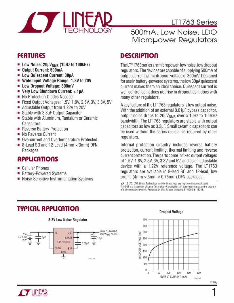
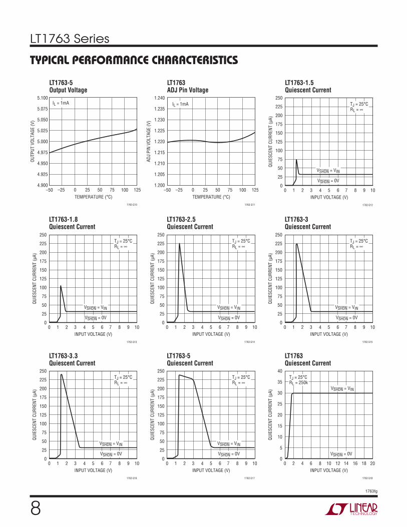
LT1763 Series 1 1763fg TYPICAL APPLICATION DESCRIPTION 500mA, Low Noise, LDO Micropower Regulators The LT ® 1763 series are micropower, low noise, low dropout regulators. The devices are capable of supplying 500mA of output current with a dropout voltage of 300mV. Designed for use in battery-powered systems, the low 30μA quiescent current makes them an ideal choice. Quiescent current is well controlled; it does not rise in dropout as it does with many other regulators. A key feature of the LT1763 regulators is low output noise. With the addition of an external 0.01μF bypass capacitor, output noise drops to 20μV RMS over a 10Hz to 100kHz bandwidth. The LT1763 regulators are stable with output capacitors as low as 3.3μF. Small ceramic capacitors can be used without the series resistance required by other regulators. Internal protection circuitry includes reverse battery protection, current limiting, thermal limiting and reverse current protection. The parts come in fixed output voltages of 1.5V, 1.8V, 2.5V, 3V, 3.3V and 5V, and as an adjustable device with a 1.22V reference voltage. The LT1763 regulators are available in 8-lead SO and 12-lead, low profile (4mm × 3mm × 0.75mm) DFN packages. 3.3V Low Noise Regulator FEATURES APPLICATIONS n Low Noise: 20μV RMS (10Hz to 100kHz) n Output Current: 500mA n Low Quiescent Current: 30μA n Wide Input Voltage Range: 1.8V to 20V n Low Dropout Voltage: 300mV n Very Low Shutdown Current: < 1μA n No Protection Diodes Needed n Fixed Output Voltages: 1.5V, 1.8V, 2.5V, 3V, 3.3V, 5V n Adjustable Output from 1.22V to 20V n Stable with 3.3μF Output Capacitor n Stable with Aluminum, Tantalum or Ceramic Capacitors n Reverse Battery Protection n No Reverse Current n Overcurrent and Overtemperature Protected n 8-Lead SO and 12-Lead (4mm × 3mm) DFN Packages n Cellular Phones n Battery-Powered Systems n Noise-Sensitive Instrumentation Systems Dropout Voltage IN SHDN 0.01μF 10μF 1763 TA01 OUT SENSE V IN 3.7V TO 20V BYP GND LT1763-3.3 3.3V AT 500mA 20μV RMS NOISE 1μF + OUTPUT CURRENT (mA) 0 DROPOUT VOLTAGE (mV) 400 350 300 250 200 150 100 50 0 400 1763 TA02 100 200 300 500 L, LT, LTC, LTM, Linear Technology and the Linear logo are registered trademarks and ThinSOT is a trademark of Linear Technology Corporation. All other trademarks are the property of their respective owners. Protected by U.S. Patents including 6144250, 6118263.
Transcript
LT1763 Series
11763fg
TYPICAL APPLICATION
DESCRIPTION
500mA, Low Noise, LDO Micropower Regulators
The LT®1763 series are micropower, low noise, low dropout regulators. The devices are capable of supplying 500mA of output current with a dropout voltage of 300mV. Designed for use in battery-powered systems, the low 30μA quiescent current makes them an ideal choice. Quiescent current is well controlled; it does not rise in dropout as it does with many other regulators.
A key feature of the LT1763 regulators is low output noise. With the addition of an external 0.01μF bypass capacitor, output noise drops to 20μVRMS over a 10Hz to 100kHz bandwidth. The LT1763 regulators are stable with output capacitors as low as 3.3μF. Small ceramic capacitors can be used without the series resistance required by other regulators.
Internal protection circuitry includes reverse battery protection, current limiting, thermal limiting and reverse current protection. The parts come in fi xed output voltages of 1.5V, 1.8V, 2.5V, 3V, 3.3V and 5V, and as an adjustable device with a 1.22V reference voltage. The LT1763 regulators are available in 8-lead SO and 12-lead, low profi le (4mm × 3mm × 0.75mm) DFN packages.
3.3V Low Noise Regulator
FEATURES
APPLICATIONS
n Low Noise: 20μVRMS (10Hz to 100kHz)n Output Current: 500mAn Low Quiescent Current: 30μAn Wide Input Voltage Range: 1.8V to 20Vn Low Dropout Voltage: 300mVn Very Low Shutdown Current: < 1μAn No Protection Diodes Neededn Fixed Output Voltages: 1.5V, 1.8V, 2.5V, 3V, 3.3V, 5Vn Adjustable Output from 1.22V to 20Vn Stable with 3.3μF Output Capacitorn Stable with Aluminum, Tantalum or Ceramic
Capacitorsn Reverse Battery Protectionn No Reverse Currentn Overcurrent and Overtemperature Protectedn 8-Lead SO and 12-Lead (4mm × 3mm) DFN
Packages
n Cellular Phonesn Battery-Powered Systemsn Noise-Sensitive Instrumentation Systems
Dropout Voltage
IN
SHDN
0.01μF
10μF
1763 TA01
OUT
SENSE
VIN3.7V TO
20V
BYPGND
LT1763-3.3
3.3V AT 500mA20μVRMS NOISE
1μF+
OUTPUT CURRENT (mA)
0
DR
OP
OU
T V
OLTA
GE (
mV
)
400
350
300
250
200
150
100
50
0400
1763 TA02
100 200 300 500
L, LT, LTC, LTM, Linear Technology and the Linear logo are registered trademarks and ThinSOT is a trademark of Linear Technology Corporation. All other trademarks are the property of their respective owners. Protected by U.S. Patents including 6144250, 6118263.
LT1763 Series
21763fg
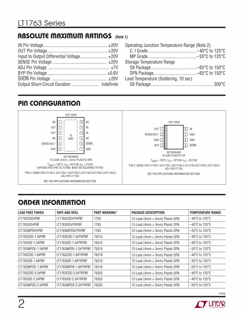
ABSOLUTE MAXIMUM RATINGSIN Pin Voltage ........................................................ ±20VOUT Pin Voltage ..................................................... ±20VInput to Output Differential Voltage ........................ ±20VSENSE Pin Voltage ............................................... ±20VADJ Pin Voltage ...................................................... ±7VBYP Pin Voltage .....................................................±0.6VSHDN Pin Voltage ................................................ ±20VOutput Short-Circuit Duration ........................ Indefi nite
(Note 1)
12
11
10
9
8
7
13GND
1
2
3
4
5
6
NC
IN
IN
NC
SHDN
GND
NC
OUT
OUT
NC
SENSE/ADJ*
BYP
TOP VIEW
DE PACKAGE12-LEAD (4mm × 3mm) PLASTIC DFN
TJMAX = 125°C, θJA = 40°C/W, θJC = 5°C/WEXPOSED PAD (PIN 13) IS GND, MUST BE SOLDERED TO PCB
*PIN 5: SENSE FOR LT1763-1.5/LT1763-1.8/LT1763-2.5/LT1763-3/LT1763-3.3/LT1763-5ADJ FOR LT1763
SEE THE APPLICATIONS INFORMATION SECTION.
TOP VIEW
IN
GND
GND
SHDN
OUT
SENSE/ADJ*
GND
BYP
S8 PACKAGE8-LEAD PLASTIC SO
1
2
3
4
8
7
6
5
TJMAX = 150°C, θJA = 70°C/W, θJC = 35°C/W
*PIN 2: SENSE FOR LT1763-1.5/LT1763-1.8/LT1763-2.5/LT1763-3/LT1763-3.3/LT1763-5ADJ FOR LT1763
SEE THE APPLICATIONS INFORMATION SECTION.
ORDER INFORMATIONLEAD FREE FINISH TAPE AND REEL PART MARKING* PACKAGE DESCRIPTION TEMPERATURE RANGE
Operating Junction Temperature Range (Note 2) C, I Grade ...........................................–40°C to 125°C MP Grade ...........................................–55°C to 125°CStorage Temperature Range S8 Package ........................................–65°C to 150°C DFN Package ......................................–65°C to 150°CLead Temperature (Soldering, 10 sec)
LT1763CS8 LT1763CS8#TR 1763 8-Lead Plastic SO –40°C to 125°C
LT1763IS8 LT1763IS8#TR 1763 8-Lead Plastic SO –40°C to 125°C
LT1763MPS8 LT1763MPS8#TR 1763MP 8-Lead Plastic SO –55°C to 125°C
LT1763CS8-1.5 LT1763CS8-1.5#TR 176315 8-Lead Plastic SO –40°C to 125°C
LT1763IS8-1.5 LT1763IS8-1.5#TR 176315 8-Lead Plastic SO –40°C to 125°C
LT1763CS8-1.8 LT1763CS8-1.8#TR 176318 8-Lead Plastic SO –40°C to 125°C
LT1763IS8-1.8 LT1763IS8-1.8#TR 176318 8-Lead Plastic SO –40°C to 125°C
LT1763CS8-2.5 LT1763CS8-2.5#TR 176325 8-Lead Plastic SO –40°C to 125°C
LT1763IS8-2.5 LT1763IS8-2.5#TR 176325 8-Lead Plastic SO –40°C to 125°C
LT1763CS8-3 LT1763CS8-3#TR 17633 8-Lead Plastic SO –40°C to 125°C
LT1763IS8-3 LT1763IS8-3#TR 17633 8-Lead Plastic SO –40°C to 125°C
LT1763CS8-3.3 LT1763CS8-3.3#TR 176333 8-Lead Plastic SO –40°C to 125°C
LT1763IS8-3.3 LT1763IS8-3.3#TR 176333 8-Lead Plastic SO –40°C to 125°C
LT1763CS8-5 LT1763CS8-5#TR 17635 8-Lead Plastic SO –40°C to 125°C
LT1763IS8-5 LT1763IS8-5#TR 17635 8-Lead Plastic SO –40°C to 125°C
Consult LTC Marketing for parts specifi ed with wider operating temperature ranges. *The temperature grade is identifi ed by a label on the shipping container.
For more information on lead free part marking, go to: http://www.linear.com/leadfree/
For more information on tape and reel specifi cations, go to: http://www.linear.com/tapeandreel/
ORDER INFORMATION
LT1763 Series
51763fg
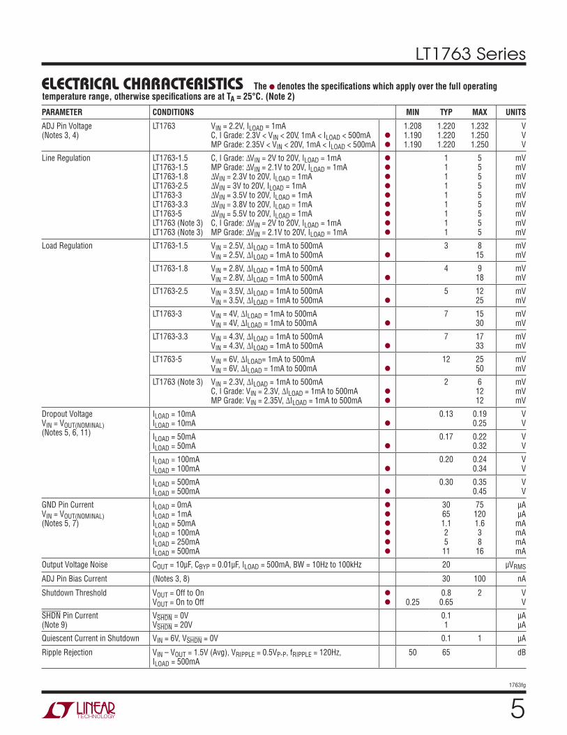
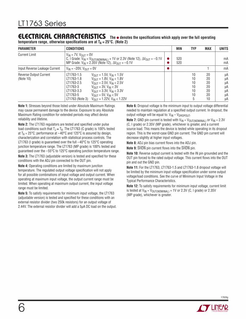
ELECTRICAL CHARACTERISTICS The l denotes the specifi cations which apply over the full operating temperature range, otherwise specifi cations are at TA = 25°C. (Note 2)
Output Noise Spectral DensityRMS Output Noise vs Bypass Capacitor
RMS Output Noise vs Load Current (10Hz to 100kHz)
FREQUENCY (Hz)
10 1k 10k 100k
1763 G49
100
10
1
0.1
0.01
OU
TP
UT N
OIS
E S
PEC
TR
AL D
EN
SIT
Y (
μV
/H
z)
LT1763
LT1763-5 CBYP = 1000pF
CBYP = 0.01μF
CBYP = 100pF
COUT = 10μFIL = 500mA
CBYP (pF)
10
OU
TP
UT N
OIS
E (
μV
RM
S)
160
140
120
100
80
60
40
20
0100 1000 10000
1763 G50
COUT = 10μFIL = 500mAf = 10Hz TO 100kHz
LT1763-5
LT1763-3.3
LT1763
LT1763-1.5
LT1763-3
LT1763-2.5
LT1763-1.8
LOAD CURRENT (mA)
0.01
OU
TP
UT N
OIS
E (
μV
RM
S)
160
140
120
100
80
60
40
20
00.1 1
1763 G51
10 100 1000
COUT = 10μF
LT1763-5
LT1763-5
LT1763
LT1763
CBYP = 0CBYP = 0.01μF
LT1763 Series
131763fg
TYPICAL PERFORMANCE CHARACTERISTICSLT1763-510Hz to 100kHz Output NoiseCBYP = 0.01μF
LT1763-5Transient ResponseCBYP = 0
LT1763-5Transient ResponseCBYP = 0.01μF
1ms/DIV
VOUT100μV/DIV
COUT = 10μFIL = 500mA
1763 G55
TIME (μs)
0.4
0.2
0
–0.2
–0.4OU
TP
UT V
OLTA
GE
DEV
IATIO
N (
V)
600
400
200
0
LO
AD
CU
RR
EN
T(m
A)
1763 G56
0 200 400 600 800 1000
VIN = 6VCIN = 10μFCOUT = 10μF
TIME (μs)
0.10
0.05
0
–0.05
–0.10OU
TP
UT V
OLTA
GE
DEV
IATIO
N (
V)
600
400
200
0
LO
AD
CU
RR
EN
T(m
A)
1763 G57
0 20 30 50 70 9010 40 60 80 100
VIN = 6VCIN = 10μFCOUT = 10μF
LT1763 Series
141763fg
PIN FUNCTIONSNC (Pins 1, 4, 9, 12) DE12 Only: No Connect. No connect pins have no connection to any internal circuitry. These pins may be tied to either GND or VIN, or left fl oating.
OUT (Pins 2, 3/Pin 1): Output. The output supplies power to the load. A minimum output capacitor of 3.3μF is re-quired to prevent oscillations. Larger output capacitors will be required for applications with large transient loads to limit peak voltage transients. See the Applications Infor-mation section for more information on output capacitance and reverse output characteristics.
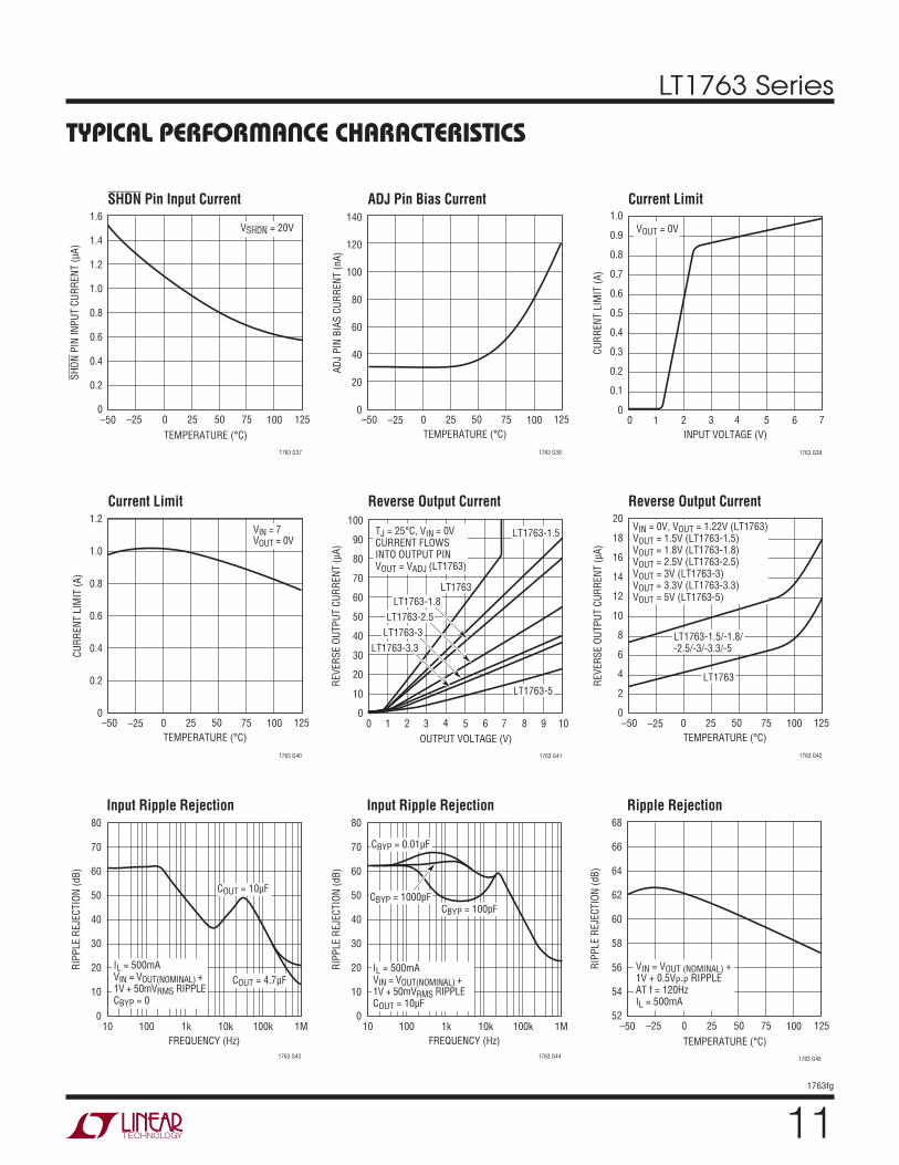
ADJ (Pin 5/Pin 2): Adjust. For the adjustable LT1763, this is the input to the error amplifi er. This pin is internally clamped to ±7V. It has a bias current of 30nA which fl ows into the pin (see the curve of ADJ Pin Bias Current vs Temperature in the Typical Performance Characteristics section). The ADJ pin voltage is 1.22V referenced to ground and the output voltage range is 1.22V to 20V.
SENSE (Pin 5/Pin 2): Output Sense. For fi xed volt-age versions of the LT1763 (LT1763-1.5/LT1763-1.8/LT1763-2.5/LT1763-3/LT1763-3.3/LT1763-5), the SENSE pin is the input to the error amplifi er. Optimum regula-tion will be obtained at the point where the SENSE pin is connected to the OUT pin of the regulator. In critical applications, small voltage drops are caused by the re-sistance (RP) of PC traces between the regulator and the load. These may be eliminated by connecting the SENSE pin to the output at the load as shown in Figure 1 (Kelvin Sense Connection).
BYP (Pin 6/Pin 4): Bypass. The BYP pin is used to bypass the reference of the LT1763 regulators to achieve low noise performance from the regulator. The BYP pin is clamped internally to ±0.6V (one VBE). A small capacitor from the output to this pin will bypass the reference to lower the output voltage noise. A maximum value of 0.01μF can be used for reducing output voltage noise to a typical 20μVRMS over a 10Hz to 100kHz bandwidth. If not used, this pin must be left unconnected.
GND (Pins 7, Exposed Pad Pin 13/Pins 3, 6, 7): Ground. The exposed pad of the DFN package is an electrical con-nection to GND. To ensure proper electrical and thermal performance, solder Pin 13 to the PCB ground and tie directly to Pin 7. Connect the bottom of the output volt-age setting resistor divider directly to the GND pins for optimum load regulation performance.
SHDN (Pin 8/Pin 5): Shutdown. The SHDN pin is used to put the LT1763 regulators into a low power shutdown state. The output will be off when the SHDN pin is pulled low. The SHDN pin can be driven either by 5V logic or open-collector logic with a pull-up resistor. The pull-up resistor is required to supply the pull-up current of the open-collector gate, normally several microamperes, and the SHDN pin current, typically 1μA. If unused, the SHDN pin must be connected to VIN. The device will be in the low power shutdown state if the SHDN pin is not connected.
IN (Pin 10, 11/Pin 8): Input. Power is supplied to the device through the IN pin. A bypass capacitor is required on this pin if the device is more than six inches away from the main input fi lter capacitor. In general, the output imped-ance of a battery rises with frequency, so it is advisable to include a bypass capacitor in battery-powered circuits. A bypass capacitor in the range of 1μF to 10μF is suffi cient. The LT1763 regulators are designed to withstand reverse voltages on the IN pin with respect to ground and the OUT pin. In the case of a reverse input, which can happen if a battery is plugged in backwards, the device will act as if there is a diode in series with its input. There will be no reverse current fl ow into the regulator and no reverse voltage will appear at the load. The device will protect both itself and the load.
(DE12/S8)
Note that the voltage drop across the external PC traces will add to the dropout voltage of the regulator. The SENSE pin bias current is 10μA at the nominal rated output voltage. The SENSE pin can be pulled below ground (as in a dual supply system where the regulator load is returned to a negative supply) and still allow the device to start and operate.
IN
SHDN
1763 F01
RPOUT
VINSENSE
GND
LT1763
RP
3
2
1
5
8
++LOAD
Figure 1. Kelvin Sense Connection
LT1763 Series
151763fg
The LT1763 series are 500mA low dropout regulators with micropower quiescent current and shutdown. The devices are capable of supplying 500mA at a dropout voltage of 300mV. Output voltage noise can be lowered to 20μVRMS over a 10Hz to 100kHz bandwidth with the addition of a 0.01μF reference bypass capacitor. Additionally, the reference bypass capacitor will improve transient response of the regulator, lowering the settling time for transient load conditions. The low operating quiescent current (30μA) drops to less than 1μA in shutdown. In addition to the low quiescent current, the LT1763 regulators incorporate several protection features which make them ideal for use in battery-powered systems. The devices are protected against both reverse input and reverse output voltages. In battery backup applications where the output can be held up by a backup battery when the input is pulled to ground, the LT1763-X acts like it has a diode in series with its output and prevents reverse current fl ow. Additionally, in dual supply applications where the regulator load is returned to a negative supply, the output can be pulled below ground by as much as 20V and still allow the device to start and operate.
Adjustable Operation
The adjustable version of the LT1763 has an output voltage range of 1.22V to 20V. The output voltage is set by the ratio of two external resistors, as shown in Figure 2. The device servos the output to maintain the ADJ pin voltage at 1.22V referenced to ground. The current in R1 is then equal to 1.22V/R1 and the current in R2 is the current in R1 plus the ADJ pin bias current. The ADJ pin bias current, 30nA at 25°C, fl ows through R2 into the ADJ pin. The output voltage can be calculated using the formula in Figure 2. The value of R1 should be no greater than 250k to minimize errors in the output voltage caused by the ADJ pin bias current. Note that in shutdown the output is turned off and the divider current will be zero. Curves of ADJ Pin Voltage vs Temperature and ADJ Pin Bias Current vs Temperature appear in the Typical Performance Characteristics section.
The adjustable device is tested and specifi ed with the ADJ pin tied to the OUT pin for an output voltage of 1.22V. Specifi cations for output voltages greater than 1.22V will be proportional to the ratio of the desired output voltage
APPLICATIONS INFORMATION
Figure 2. Adjustable Operation
to 1.22V: VOUT/1.22V. For example, load regulation for an output current change of 1mA to 500mA is –2mV typical at VOUT = 1.22V. At VOUT = 12V, load regulation is:
(12V/1.22V)(–2mV) = –19.6mV
Bypass Capacitance and Low Noise Performance
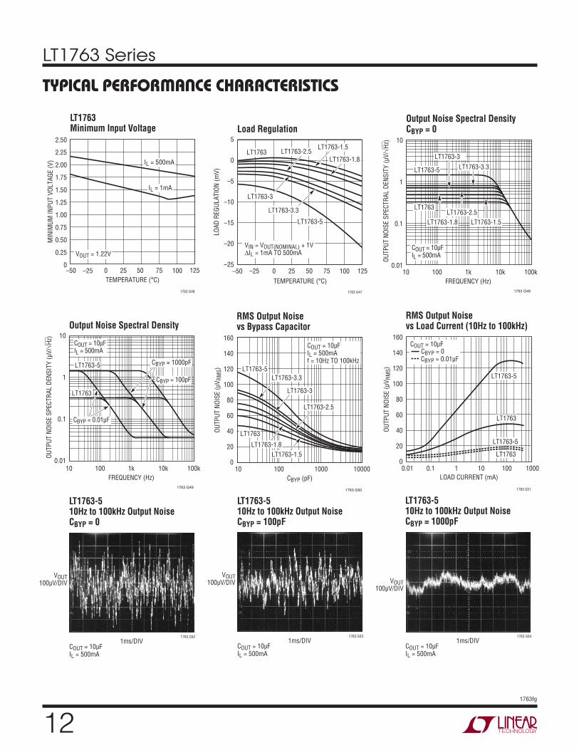
The LT1763 regulators may be used with the addition of a bypass capacitor from VOUT to the BYP pin to lower output voltage noise. A good quality low leakage capacitor is recommended. This capacitor will bypass the reference of the regulator, providing a low frequency noise pole. The noise pole provided by this bypass capacitor will lower the output voltage noise to as low as 20μVRMS with the addition of a 0.01μF bypass capacitor. Using a bypass capacitor has the added benefi t of improving transient response. With no bypass capacitor and a 10μF output capacitor, a 10mA to 500mA load step will settle to within 1% of its fi nal value in less than 100μs. With the addition of a 0.01μF bypass capacitor, the output will settle to within 1% for a 10mA to 500mA load step in less than 10μs, with total output voltage deviation of less than 2.5% (see the LT1763-5 Transient Response curve in the Typical Performance Characteristics section). However, regulator start-up time is proportional to the size of the bypass capacitor, slowing to 15ms with a 0.01μF bypass capacitor and 10μF output capacitor.
IN
1763 F02
R2
OUT
VIN
VOUT
ADJGND
LT1763
R1
+
V VRR
I R
V VI nA
OUT ADJ
ADJ
ADJ
= +⎛⎝⎜
⎞⎠⎟ + ( )( )
=
= °
1 22 121
2
1 2230
.
. AT 25 C
OUTPUT RANGE = 1.22V TO 20V
LT1763 Series
161763fg
Output Capacitance and Transient Response
The LT1763 regulators are designed to be stable with a wide range of output capacitors. The ESR of the output capacitor affects stability, most notably with small capaci-tors. A minimum output capacitor of 3.3μF with an ESR of 3Ω, or less, is recommended to prevent oscillations. The LT1763-X is a micropower device and output transient response will be a function of output capacitance. Larger values of output capacitance decrease the peak deviations and provide improved transient response for larger load current changes. Bypass capacitors, used to decouple individual components powered by the LT1763-X, will increase the effective output capacitor value. With larger capacitors used to bypass the reference (for low noise operation), larger values of output capacitors are needed. For 100pF of bypass capacitance, 4.7μF of output capaci-tor is recommended. With a 1000pF bypass capacitor or larger, a 6.8μF output capacitor is recommended.
The shaded region of Figure 3 defi nes the range over which the LT1763 regulators are stable. The minimum ESR needed is defi ned by the amount of bypass capacitance used, while the maximum ESR is 3Ω.
Extra consideration must be given to the use of ceramic capacitors. Ceramic capacitors are manufactured with a variety of dielectrics, each with different behavior across temperature and applied voltage. The most common dielectrics used are specifi ed with EIA temperature characteristic codes of Z5U, Y5V, X5R and X7R. The Z5U and Y5V dielectrics are good for providing high capacitances in a small package, but they tend to have strong voltage and temperature coeffi cients, as shown in Figures 4 and 5. When used with a 5V regulator, a 16V 10μF Y5V capacitor can exhibit an effective value as low as 1μF to 2μF for the DC bias voltage applied and over the operating temperature range. The X5R and X7R dielectrics result in more stable characteristics and are more suitable for use as the output capacitor. The X7R type has better stability across temperature, while the X5R is less expensive and is available in higher values. Care still must be exercised when using X5R and X7R capacitors; the X5R and X7R codes only specify operating temperature range and maximum capacitance change over temperature. Capacitance change due to DC bias with X5R and X7R capacitors is better than
APPLICATIONS INFORMATION
OUTPUT CAPACITANCE (μF)
1
ES
R (
Ω)
4.0
3.5
3.0
2.5
2.0
1.5
1.0
0.5
03 10
1763 F03
2 4 5 6 7 8 9
STABLE REGION
CBYP = 330pFCBYP 1000pF
CBYP = 100pF
CBYP = 0
Figure 3. Stability
DC BIAS VOLTAGE (V)
CH
AN
GE I
N V
ALU
E (
%)
1763 F04
20
0
–20
–40
–60
–80
–1000 4 8 102 6 12 14
X5R
Y5V
16
BOTH CAPACITORS ARE 16V,1210 CASE SIZE, 10μF
TEMPERATURE (°C)
–50
40
20
0
–20
–40
–60
–80
–10025 75
1763 F05
–25 0 50 100 125
Y5V
CH
AN
GE I
N V
ALU
E (
%)
X5R
BOTH CAPACITORS ARE 16V,1210 CASE SIZE, 10μF
Figure 4. Ceramic Capacitor DC Bias Characteristics
Figure 5. Ceramic Capacitor Temperature Characteristics
LT1763 Series
171763fg
Figure 6. Noise Resulting from Tapping on a Ceramic Capacitor
Y5V and Z5U capacitors, but can still be signifi cant enough to drop capacitor values below appropriate levels. Capacitor DC bias characteristics tend to improve as component case size increases, but expected capacitance at operating voltage should be verifi ed.
Voltage and temperature coeffi cients are not the only sources of problems. Some ceramic capacitors have a piezoelectric response. A piezoelectric device generates voltage across its terminals due to mechanical stress, similar to the way a piezoelectric accelerometer or microphone works. For a ceramic capacitor, the stress can be induced by vibrations in the system or thermal transients. The resulting voltages produced can cause appreciable amounts of noise, especially when a ceramic capacitor is used for noise bypassing. A ceramic capacitor produced Figure 6’s trace in response to light tapping from a pencil. Similar vibration induced behavior can masquerade as increased output voltage noise.
Thermal Considerations
The power handling capability of the device will be limited by the maximum rated junction temperature (125°C). The power dissipated by the device will be made up of two components:
1. Output current multiplied by the input/output voltage differential: (IOUT)(VIN – VOUT), and
2. GND pin current multiplied by the input voltage: (IGND)(VIN).
The GND pin current can be found by examining the GND Pin Current curves in the Typical Performance Character-istics section. Power dissipation will be equal to the sum of the two components listed above.
The LT1763 series regulators have internal thermal limiting designed to protect the device during overload conditions. For continuous normal conditions, the maximum junction temperature rating of 125°C must not be exceeded. It is important to give careful consideration to all sources of thermal resistance from junction-to-ambient. Additional heat sources mounted nearby must also be considered.
For surface mount devices, heat sinking is accomplished by using the heat spreading capabilities of the PC board and its copper traces. Copper board stiffeners and plated through-holes can also be used to spread the heat gener-ated by power devices.
The following tables list thermal resistance for several different board sizes and copper areas. All measurements were taken in still air on 3/32" FR-4 board with one ounce
copper.
Table 1. DE Package, 12-Lead DFN
COPPER AREA
BOARD AREATHERMAL RESISTANCE
(JUNCTION-TO-AMBIENT)TOPSIDE* BACKSIDE
2500mm2 2500mm2 2500mm2 40°C/W
1000mm2 2500mm2 2500mm2 45°C/W
225mm2 2500mm2 2500mm2 50°C/W
100mm2 2500mm2 2500mm2 60°C/W
* Device is mounted on topside
APPLICATIONS INFORMATION
100ms/DIV
VOUT500μV/DIV
1763 F06
LT1763-5COUT = 10μFCBYP = 0.01μFILOAD = 100mA
LT1763 Series
181763fg
APPLICATIONS INFORMATIONTable 2. SO-8 Package, 8-Lead SO
COPPER AREA
BOARD AREATHERMAL RESISTANCE
(JUNCTION-TO-AMBIENT)TOPSIDE* BACKSIDE
2500mm2 2500mm2 2500mm2 60°C/W
1000mm2 2500mm2 2500mm2 60°C/W
225mm2 2500mm2 2500mm2 68°C/W
100mm2 2500mm2 2500mm2 74°C/W
50mm2 2500mm2 2500mm2 86°C/W
* Device is mounted on topside
Calculating Junction Temperature
Example: Given an output voltage of 3.3V, an input voltage range of 4V to 6V, an output current range of 0mA to 250mA and a maximum ambient temperature of 50°C, what will the maximum junction temperature be?
The power dissipated by the device will be equal to:
IOUT(MAX)(VIN(MAX) – VOUT) + IGND(VIN(MAX))
where,
IOUT(MAX) = 250mA VIN(MAX) = 6V IGND at (IOUT = 250mA, VIN = 6V) = 5mA So,
P = 250mA(6V – 3.3V) + 5mA(6V) = 0.71W
The thermal resistance will be in the range of 60°C/W to 86°C/W, depending on the copper area. So, the junction temperature rise above ambient will be approximately equal to:
0.71W(75°C/W) = 53.3°C
The maximum junction temperature will then be equal to the maximum junction temperature rise above ambient plus the maximum ambient temperature, or :
TJMAX = 50°C + 53.3°C = 103.3°C
Protection Features
The LT1763 regulators incorporate several protection features which make them ideal for use in battery-powered circuits. In addition to the normal protection features associated with monolithic regulators, such as current limiting and thermal limiting, the devices are protected against reverse input voltages, reverse output voltages and reverse voltages from output to input.
Current limit protection and thermal overload protection are intended to protect the device against current overload conditions at the output of the device. For normal operation, the junction temperature should not exceed 125°C.
The input of the device will withstand reverse voltages of 20V. Current fl ow into the device will be limited to less than 1mA (typically less than 100μA) and no negative voltage will appear at the output. The device will protect both itself and the load. This provides protection against batteries which can be plugged in backward.
The output of the LT1763-X can be pulled below ground without damaging the device. If the input is left open-circuit or grounded, the output can be pulled below ground by 20V. For fi xed voltage versions, the output will act like a large resistor, typically 500k or higher, limiting current fl ow to less than 100μA. For adjustable versions, the output will act like an open circuit; no current will fl ow out of the pin. If the input is powered by a voltage source, the output will source the short-circuit current of the device and will protect itself by thermal limiting. In this case, grounding the SHDN pin will turn off the device and stop the output from sourcing the short-circuit current.
The ADJ pin of the adjustable device can be pulled above or below ground by as much as 7V without damaging the device. If the input is left open-circuit or grounded, the ADJ pin will act like an open circuit when pulled below ground and like a large resistor (typically 100k) in series with a diode when pulled above ground.
In situations where the ADJ pin is connected to a resistor divider that would pull the ADJ pin above its 7V clamp voltage if the output is pulled high, the ADJ pin input current must be limited to less than 5mA. For example, a resistor divider is used to provide a regulated 1.5V output from the 1.22V reference when the output is forced to 20V.
LT1763 Series
191763fg
Figure 7. Reverse Output Current
The top resistor of the resistor divider must be chosen to limit the current into the ADJ pin to less than 5mA when the ADJ pin is at 7V. The 13V difference between output and ADJ pin divided by the 5mA maximum current into the ADJ pin yields a minimum top resistor value of 2.6k.
In circuits where a backup battery is required, several different input/output conditions can occur. The output voltage may be held up while the input is either pulled to ground, pulled to some intermediate voltage or is left open-circuit. Current fl ow back into the output will follow the curve shown in Figure 7.
When the IN pin of the LT1763-X is forced below the OUT pin, or the OUT pin is pulled above the IN pin, input cur-rent will typically drop to less than 2μA. This can happen if the input of the device is connected to a discharged (low voltage) battery and the output is held up by either a backup battery or a second regulator circuit. The state of the SHDN pin will have no effect on the reverse output current when the output is pulled above the input.
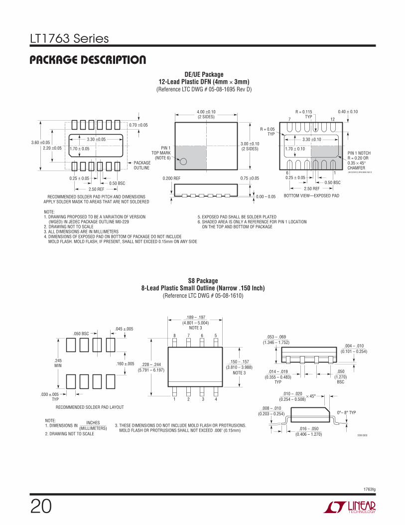
S8 Package8-Lead Plastic Small Outline (Narrow .150 Inch)
(Reference LTC DWG # 05-08-1610)
.016 – .050
(0.406 – 1.270)
.010 – .020
(0.254 – 0.508) 45°
0°– 8° TYP.008 – .010
(0.203 – 0.254)
SO8 0303
.053 – .069
(1.346 – 1.752)
.014 – .019
(0.355 – 0.483)TYP
.004 – .010
(0.101 – 0.254)
.050
(1.270)BSC
1 2 3 4
.150 – .157
(3.810 – 3.988)
NOTE 3
8 7 6 5
.189 – .197
(4.801 – 5.004)NOTE 3
.228 – .244
(5.791 – 6.197)
.245MIN .160 ±.005
RECOMMENDED SOLDER PAD LAYOUT
.045 ±.005.050 BSC
.030 ±.005 TYP
INCHES
(MILLIMETERS)
NOTE:1. DIMENSIONS IN
2. DRAWING NOT TO SCALE
3. THESE DIMENSIONS DO NOT INCLUDE MOLD FLASH OR PROTRUSIONS. MOLD FLASH OR PROTRUSIONS SHALL NOT EXCEED .006" (0.15mm)
4.00 0.10(2 SIDES)
3.00 0.10(2 SIDES)
NOTE:1. DRAWING PROPOSED TO BE A VARIATION OF VERSION (WGED) IN JEDEC PACKAGE OUTLINE M0-2292. DRAWING NOT TO SCALE3. ALL DIMENSIONS ARE IN MILLIMETERS4. DIMENSIONS OF EXPOSED PAD ON BOTTOM OF PACKAGE DO NOT INCLUDE MOLD FLASH. MOLD FLASH, IF PRESENT, SHALL NOT EXCEED 0.15mm ON ANY SIDE
5. EXPOSED PAD SHALL BE SOLDER PLATED6. SHADED AREA IS ONLY A REFERENCE FOR PIN 1 LOCATION ON THE TOP AND BOTTOM OF PACKAGE
0.40 0.10
BOTTOM VIEW—EXPOSED PAD
1.70 0.10
0.75 0.05
R = 0.115TYP
R = 0.05TYP
2.50 REF
16
127
PIN 1 NOTCHR = 0.20 OR0.35 45CHAMFER
PIN 1TOP MARK
(NOTE 6)
0.200 REF
0.00 – 0.05
(UE12/DE12) DFN 0806 REV D
2.50 REF
RECOMMENDED SOLDER PAD PITCH AND DIMENSIONSAPPLY SOLDER MASK TO AREAS THAT ARE NOT SOLDERED
2.20 0.05
0.70 0.05
3.60 0.05
PACKAGEOUTLINE
3.30 0.10
0.25 0.050.50 BSC
1.70 0.05
3.30 0.05
0.50 BSC0.25 0.05
LT1763 Series
211763fg
Information furnished by Linear Technology Corporation is believed to be accurate and reliable. However, no responsibility is assumed for its use. Linear Technology Corporation makes no representa-tion that the interconnection of its circuits as described herein will not infringe on existing patent rights.
REVISION HISTORYREV DATE DESCRIPTION PAGE NUMBER
G 5/10 Updated Order Information to add MP-grade to all versions of DFN package
Revised Line Regulation section of Electrical Characteristics
Consolidated GND and exposed pad descriptions in Pin Descriptions section