LTC2310-14 1 231014f For more information www.linear.com/LTC2310-14 TYPICAL APPLICATION FEATURES DESCRIPTION 14-Bit + Sign, 2Msps Differential Input ADC with Wide Input Common Mode Range The LTC ® 2310-14 is a low noise, high speed 14-bit + sign successive approximation register (SAR) ADC with differential inputs and wide input common mode range. Operating from a single 3.3V or 5V supply, the LTC2310-14 has an 8V P-P differential input range, making it ideal for applications which require a wide dynamic range with high common mode rejection. The LTC2310-14 achieves ±2.5LSB INL guaranteed, no missing codes at 14 bits and 82dB SNR typical. The LTC2310-14 has an onboard low drift (20ppm/°C max) 2.048V or 4.096V temperature-compensated reference and provides an external 1.25V buffered reference input. The LTC2310-14 also has a high speed SPI-compatible serial interface that supports CMOS or LVDS. The fast 2Msps throughput with no cycle latency makes the LTC2310-14 ideally suited for a wide variety of high speed applications. The LTC2310-14 dissipates only 35mW with a 5V supply and offers nap and sleep modes to reduce the power consumption for further power savings during inactive periods. 32k Point FFT f SMPL = 2Msps, f IN = 500kHz APPLICATIONS n 2Msps Throughput Rate n ±2.5LSB INL Guaranteed n Guaranteed 14-Bit, No Missing Codes n 8V P-P Differential Inputs with Wide Input Common Mode Range n 82dB SNR (Typ) at f IN = 500kHz n –93dB THD (Typ) at f IN = 500kHz n No Cycle Latency n Guaranteed Operation –40°C to 125°C n Single 3.3V or 5V Supply n Low Drift (20ppm/°C Max) 2.048V or 4.096V Internal Reference with 1.25V External Reference Input n 1.8V to 2.5V I/O Voltages n CMOS or LVDS SPI-Compatible Serial I/O n Power Dissipation 35mW at V DD = 5V (Typ) n Small 16-Lead (4mm × 5mm) MSOP Package n High Speed Data Acquisition Systems n Communications n Remote Data Acquisition n Imaging n Optical Networking n Automotive n Multiphase Motor Control L, LT, LTC, LTM, Linear Technology and the Linear logo are registered trademarks of Linear Technology Corporation. All other trademarks are the property of their respective owners. BIPOLAR 25Ω 25Ω 47pF UNIPOLAR ARBITRARY DIFFERENTIAL INPUTS NO CONFIGURATION REQUIRED IN + , IN – DIFFERENTIAL OV DD V DD LTC2310-14 GND 1.8V TO 2.5V 231014 TA01a 1μF 3.3V OR 5V 0V 0V 0V 0V V DD V DD V DD V DD REFIN REFOUT SDO A IN – A IN + SCK CNV CMOS/LVDS 1μF LVDS OR CMOS CONFIGURABLE I/O 10μF 10μF SNR = 82dB THD = –93dB SINAD = 81.7dB SFDR = 97dB FREQUENCY (MHz) 0 0.2 0.4 0.6 0.8 1.0 –140 –120 –100 –80 –60 –40 –20 0 AMPLITUDE (dBFS) 231014 TA01b
Transcript
LTC2310-14
1231014f
For more information www.linear.com/LTC2310-14
Typical applicaTion
FeaTures DescripTion
14-Bit + Sign, 2MspsDifferential Input ADC with Wide
Input Common Mode Range
The LTC®2310-14 is a low noise, high speed 14-bit + sign successive approximation register (SAR) ADC with differential inputs and wide input common mode range. Operating from a single 3.3V or 5V supply, the LTC2310-14 has an 8VP-P differential input range, making it ideal for applications which require a wide dynamic range with high common mode rejection. The LTC2310-14 achieves ±2.5LSB INL guaranteed, no missing codes at 14 bits and 82dB SNR typical.
The LTC2310-14 has an onboard low drift (20ppm/°C max) 2.048V or 4.096V temperature-compensated reference and provides an external 1.25V buffered reference input. The LTC2310-14 also has a high speed SPI-compatible serial interface that supports CMOS or LVDS. The fast 2Msps throughput with no cycle latency makes the LTC2310-14 ideally suited for a wide variety of high speed applications. The LTC2310-14 dissipates only 35mW with a 5V supply and offers nap and sleep modes to reduce the power consumption for further power savings during inactive periods.
32k Point FFT fSMPL = 2Msps, fIN = 500kHz
applicaTions
n 2Msps Throughput Rate n ±2.5LSB INL Guaranteed n Guaranteed 14-Bit, No Missing Codes n 8VP-P Differential Inputs with Wide Input Common
Mode Range n 82dB SNR (Typ) at fIN = 500kHz n –93dB THD (Typ) at fIN = 500kHz n No Cycle Latency n Guaranteed Operation –40°C to 125°C n Single 3.3V or 5V Supply n Low Drift (20ppm/°C Max) 2.048V or 4.096V Internal
Reference with 1.25V External Reference Input n 1.8V to 2.5V I/O Voltages n CMOS or LVDS SPI-Compatible Serial I/O n Power Dissipation 35mW at VDD = 5V (Typ) n Small 16-Lead (4mm × 5mm) MSOP Package
n High Speed Data Acquisition Systems n Communications n Remote Data Acquisition n Imaging n Optical Networking n Automotive n Multiphase Motor Control
L, LT, LTC, LTM, Linear Technology and the Linear logo are registered trademarks of Linear Technology Corporation. All other trademarks are the property of their respective owners.
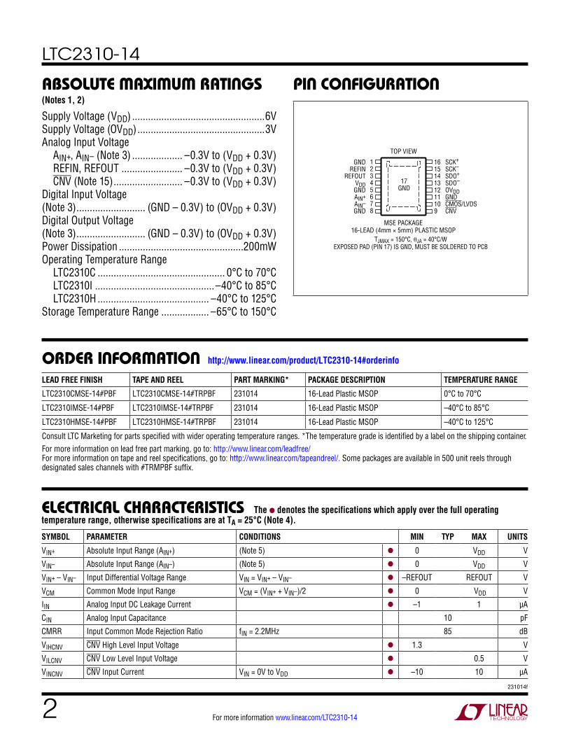
Supply Voltage (VDD) ..................................................6VSupply Voltage (OVDD) ................................................3VAnalog Input Voltage AIN+, AIN– (Note 3) ................... –0.3V to (VDD + 0.3V) REFIN, REFOUT ....................... –0.3V to (VDD + 0.3V) CNV (Note 15) .......................... –0.3V to (VDD + 0.3V)Digital Input Voltage(Note 3) .......................... (GND – 0.3V) to (OVDD + 0.3V)Digital Output Voltage(Note 3) .......................... (GND – 0.3V) to (OVDD + 0.3V)Power Dissipation ...............................................200mWOperating Temperature Range LTC2310C ................................................ 0°C to 70°C LTC2310I .............................................–40°C to 85°C LTC2310H .......................................... –40°C to 125°CStorage Temperature Range .................. –65°C to 150°C
(Notes 1, 2)
12345678
GNDREFIN
REFOUTVDDGNDAIN+AIN–GND
161514131211109
17GND
SCK+
SCK–
SDO+
SDO–
OVDDGNDCMOS/LVDSCNV
TOP VIEW
MSE PACKAGE16-LEAD (4mm × 5mm) PLASTIC MSOP
TJMAX = 150°C, θJA = 40°C/W EXPOSED PAD (PIN 17) IS GND, MUST BE SOLDERED TO PCB
LEAD FREE FINISH TAPE AND REEL PART MARKING* PACKAGE DESCRIPTION TEMPERATURE RANGE
LTC2310CMSE-14#PBF LTC2310CMSE-14#TRPBF 231014 16-Lead Plastic MSOP 0°C to 70°C
LTC2310IMSE-14#PBF LTC2310IMSE-14#TRPBF 231014 16-Lead Plastic MSOP –40°C to 85°C
LTC2310HMSE-14#PBF LTC2310HMSE-14#TRPBF 231014 16-Lead Plastic MSOP –40°C to 125°C
Consult LTC Marketing for parts specified with wider operating temperature ranges. *The temperature grade is identified by a label on the shipping container.For more information on lead free part marking, go to: http://www.linear.com/leadfree/ For more information on tape and reel specifications, go to: http://www.linear.com/tapeandreel/. Some packages are available in 500 unit reels through designated sales channels with #TRMPBF suffix.
elecTrical characTerisTics
SYMBOL PARAMETER CONDITIONS MIN TYP MAX UNITS
VIN+ Absolute Input Range (AIN+) (Note 5) l 0 VDD V
VIN– Absolute Input Range (AIN–) (Note 5) l 0 VDD V
VIN+ – VIN– Input Differential Voltage Range VIN = VIN+ – VIN– l –REFOUT REFOUT V
VCM Common Mode Input Range VCM = (VIN+ + VIN–)/2 l 0 VDD V
IIN Analog Input DC Leakage Current l –1 1 µA
CIN Analog Input Capacitance 10 pF
CMRR Input Common Mode Rejection Ratio fIN = 2.2MHz 85 dB
VIHCNV CNV High Level Input Voltage l 1.3 V
VILCNV CNV Low Level Input Voltage l 0.5 V
VINCNV CNV Input Current VIN = 0V to VDD l –10 10 µA
The l denotes the specifications which apply over the full operating temperature range, otherwise specifications are at TA = 25°C (Note 4).
orDer inForMaTion http://www.linear.com/product/LTC2310-14#orderinfo
SINAD Signal-to-(Noise + Distortion) Ratio fIN = 500kHz, VREFOUT = 4.096V, Internal Reference fIN = 500kHz, VREFOUT = 5V, External Reference
l 75.5 81.7 82
dB dB
SNR Signal-to-Noise Ratio fIN = 500kHz, VREFOUT = 4.096V, Internal Reference fIN = 500kHz, VREFOUT = 5V, External Reference
l 76 82 82.6
dB dB
THD Total Harmonic Distortion fIN = 500kHz, VREFOUT = 4.096V, Internal Reference fIN = 500kHz, VREFOUT = 5V, External Reference
l –93 –90
–78 dB dB
SFDR Spurious Free Dynamic Range fIN = 500kHz, VREFOUT = 4.096V, Internal Reference fIN = 500kHz, VREFOUT = 5V, External Reference
l 78 97 95
dB dB
–3dB Input Bandwidth 100 MHz
Aperture Delay 500 ps
Aperture Jitter 1 psRMS
Transient Response Full-Scale Step 3 ns
The l denotes the specifications which apply over the full operating temperature range, otherwise specifications are at TA = 25°C (Note 4).
The l denotes the specifications which apply over the full operating temperature range, otherwise specifications are at TA = 25°C and AIN = –1dBFS (Notes 4, 8).
inTernal reFerence characTerisTicsSYMBOL PARAMETER CONDITIONS MIN TYP MAX UNITS
The l denotes the specifications which apply over the full operating temperature range, otherwise specifications are at TA = 25°C (Note 4).
inTernal reFerence characTerisTics The l denotes the specifications which apply over the full operating temperature range, otherwise specifications are at TA = 25°C (Note 4).
power requireMenTs The l denotes the specifications which apply over the full operating temperature range, otherwise specifications are at TA = 25°C (Note 4).
aDc TiMing characTerisTicsSYMBOL PARAMETER CONDITIONS MIN TYP MAX UNITS
CMOS, LVDS I/O Modes
fSMPL Maximum Sampling Frequency l 2 Msps
tCYC Time Between Conversions (Note 11) l 500 1000000 ns
tACQ Acquisition Time (Note 11) l 280 ns
tCONV Conversion Time l 220 ns
tREADOUT Readout Time l 250 ns
tCNVH CNV High Time l 30 ns
tDCNVSCKL SCK Quiet Time from CNV↓ (Note 11) l 220 ns
tDSCKLCNVH SCK Delay Time to CNV↑ (Note 11) l 0 ns
tSCK SCK Period (Notes 12, 13) l 15.6 ns
tSCKH SCK High Time l 5 ns
tSCKL SCK Low Time l 5 ns
The l denotes the specifications which apply over the full operating temperature range, otherwise specifications are at TA = 25°C (Note 4).
SYMBOL PARAMETER CONDITIONS MIN TYP MAX UNITS
VDD Supply Voltage 5V Operation 3.3V Operation
l
l
4.75 3.13
5.25 3.47
V V
OVDD Supply Voltage l 1.71 2.63 V
IVDD Supply Current 2Msps Sample Rate (AIN+ = AIN– = 0V) l 6.8 11 mA
INAP Nap Mode Current Conversion Done (IVDD) l 2.8 4 mA
ISLEEP Sleep Mode Current VDD = 3.3V, Sleep Mode (IVDD + IOVDD) l 0.1 10 μA
CMOS I/O Mode
IOVDD Supply Current 2Msps Sample Rate (CL = 5pF) l 0.5 1 mA
Note 1: Stresses beyond those listed under Absolute Maximum Ratings may cause permanent damage to the device. Exposure to any Absolute Maximum Rating condition for extended periods may affect device reliability and lifetime.Note 2: All voltage values are with respect to ground.Note 3: When these pin voltages are taken below ground, or above VDD or OVDD, they will be clamped by internal diodes. This product can handle input currents up to 100mA below ground, or above VDD or OVDD, without latch-up.Note 4: VDD = 5V, OVDD = 2.5V, REFOUT = 4.096V, fSMPL = 2MHz.Note 5: Recommended operating conditions.Note 6: Integral nonlinearity is defined as the deviation of a code from a straight line passing through the actual endpoints of the transfer curve. The deviation is measured from the center of the quantization band.Note 7: Bipolar zero error is the offset voltage measured from –0.5LSB when the output code flickers between 0000 0000 0000 000 and 1111 1111 1111 111. Full-scale bipolar error is the worst-case of –FS or +FS
untrimmed deviation from ideal first and last code transitions and includes the effect of offset error. Note 8: All specifications in dB are referred to a full-scale ±4.096V input with REFOUT = 4.096V.Note 9: When REFOUT is overdriven, the internal reference buffer must be turned off by setting REFIN = 0V.Note 10: fSMPL = 2MHz, IREFOUT varies proportionally with sample rate.Note 11: Guaranteed by design, not subject to test.Note 12: Parameter tested and guaranteed at OVDD = 1.71V and OVDD = 2.5V.Note 13: tSCK of 15.6ns minimum allows a shift clock frequency up to 64MHz for falling edge capture. Note 14: Temperature coefficient is calculated by dividing the maximum change in output voltage by the specified temperature range.Note 15: CNV is driven from a low jitter digital source, typically at OVDD logic levels. This input pin has a TTL style input that will draw a small amount of current.
Figure 1. Voltage Levels for Timing Specifications
0.8 • OVDD
0.2 • OVDD
50% 50%
231014 F01
0.2 • OVDD
0.8 • OVDD
0.2 • OVDD
0.8 • OVDD
tDELAY
tWIDTH
tDELAY
aDc TiMing characTerisTics
SYMBOL PARAMETER CONDITIONS MIN TYP MAX UNITS
tDSCKSDOV SDO Data Valid Delay from SCK↓ CL = 5pF (Note 11) l 4 7.4 ns
tHSDO SDO Data Remains Valid Delay from SCK↓
CL = 5pF (Note 11) l 2 ns
tDCNVSDOV Bus Acquisition Time from CNV↓ CL = 5pF (Note 11) l 2.5 5 ns
tDCNVSDOZ Bus Relinquish Time After CNV↑ (Note 11) l 5 ns
tWAKE REFOUT Wake-Up Time CREFOUT = 10μF 10 ms
The l denotes the specifications which apply over the full operating temperature range, otherwise specifications are at TA = 25°C (Note 4).
pin FuncTionsGND (Pins 1, 5, 8, 11): Ground. These pins and the exposed pad (Pin 17) must be tied directly to a solid ground plane.
REFIN (Pin 2): Reference Buffer 1.25V Input/Output. An onboard buffer nominally outputs 1.25V to this pin. This pin should be decoupled closely to the pin (no vias) with a 10μF (X5R, 0805 size) ceramic capacitor. The internal buffer driving this pin may be overdriven with an external reference. The REFIN pin, when pulled to GND disables the REFOUT pin buffer allowing an external reference to drive REFOUT directly.
REFOUT (Pin 3): Reference Buffer Output. An onboard buffer nominally outputs 4.096V to this pin. This pin should be decoupled closely to the pin (no vias) with a 10μF (X5R, 0805 size) ceramic capacitor. The internal buffer driving this pin may be disabled by grounding the REFIN pin. If the buffer is disabled, an external reference may drive this pin in the range of 1.25V to VDD.
VDD (Pin 4): Power Supply. Bypass VDD to GND with a 1µF ceramic capacitor close to the VDD pin.
AIN+, AIN– (Pins 6, 7): Analog Differential Input Pins. Full-scale range (AIN+ to AIN–) is ±REFOUT voltage. These pins can be driven from VDD to GND.
CNV (Pin 9): Convert Input. When this pin is driven low, the conversion phase is initiated and output data is clocked out after the conversion delay (tCONV). This input pin is a TTL style input typically driven at OVDD levels with a low jitter pulse, but it is bound to VDD levels. This pin is unaf-fected by the CMOS/LVDS pin.
CMOS/LVDS (Pin 10): I/O mode select. Ground this pin to enable CMOS mode, tie to OVDD to enable LVDS mode. Float this pin to enable low power LVDS mode.
OVDD (Pin 12): I/O Interface Digital Power. The range of OVDD is 1.71V to 2.5V. This supply is nominally set to the same supply as the host interface (CMOS: 1.8V or 2.5V, LVDS: 2.5V). Bypass OVDD to GND with a 1μF ceramic capacitor close to the OVDD pin.
Exposed Pad (Pin 17): Ground. Solder this pad to ground.
CMOS I/O Mode
SDO+ (Pin 14): Serial Data Output. The conversion result is shifted MSB first on each falling edge of SCK. The result is output on SDO+. The logic level is determined by OVDD. Do not connect SDO– (Pin 13).
SCK+ (Pin 16): Serial Data Clock Input. The falling edge of this clock shifts the conversion result MSB first onto the SDO pins. Drive SCK+ with a single-ended clock. The logic level is determined by OVDD. Do not connect SCK– (Pin 15).
LVDS I/O Mode
SDO+, SDO– (Pins 14, 13): Serial Data Output. The con-version result is shifted MSB first on each falling edge of SCK. The result is output differentially on SDO+ and SDO–. These pins must be differentially terminated by an external 100Ω resistor at the receiver (FPGA).
SCK+, SCK– (Pins 16, 15): Serial Data Clock Input. The falling edge of this clock shifts the conversion result MSB first onto the SDO pins. Drive SCK+ and SCK– with a dif-ferential clock. These pins must be differentially terminated by an external 100Ω resistor at the receiver (ADC).
The LTC2310-14 is a low noise, high speed 14-bit + sign successive approximation register (SAR) ADC with dif-ferential inputs and a wide input common mode range. Operating from a single 3.3V or 5V supply, the LTC2310-14 has an 8VP-P differential input range, making it ideal for applications which require a wide dynamic range. The LTC2310-14 achieves ±2LSB INL guaranteed, no missing codes at 14 bits and 82dB SNR typical.
The LTC2310-14 has an onboard reference buffer and low drift (20ppm/°C max) 4.096V temperature-compensated reference. The LTC2310-14 also has a high speed SPI-compatible serial interface that supports CMOS or LVDS. The fast 2Msps throughput with no cycle latency makes the LTC2310-14 ideally suited for a wide variety of high speed applications. The LTC2310-14 dissipates only 35mW operating at a 5V supply. Nap and sleep modes are also pro-vided to reduce the power consumption of the LTC2310-14 during inactive periods for further power savings.
CONVERTER OPERATION
The LTC2310-14 operates in two phases. During the acquisition phase, the sample capacitor is connected to the analog input pins AIN+ and AIN– to sample the dif-ferential analog input voltage, as shown in Figure 3. A falling edge on the CNV pin initiates a conversion. Dur-ing the conversion phase, the 15-bit CDAC is sequenced through a successive approximation algorithm for each input SCK pulse, effectively comparing the sampled input
with binary-weighted fractions of the reference voltage (e.g., VREFOUT/2, VREFOUT/4 … VREFOUT/32768) using a differential comparator. At the end of conversion, the CDAC output approximates the sampled analog input. The ADC control logic then prepares the 15-bit digital output code for serial transfer. The data is clocked out on each falling edge of the SCK input clock.
TRANSFER FUNCTION
The LTC2310-14 digitizes the full-scale voltage of 2 × REFOUT into 215 levels, resulting in an LSB size of 250µV with REFOUT = 4.096V. The ideal transfer function is shown in Figure 2. The output data is in 2’s comple-ment format.
Analog Input
The differential inputs of the LTC2310-14 provide great flexibility to convert a wide variety of analog signals with no configuration required. The LTC2310-14 digitizes the difference voltage between the AIN+ and AIN– pins while supporting a wide common mode input range. The analog input signals can have an arbitrary relationship to each other, provided that they remain between VDD and GND. The LTC2310-14 can also digitize more limited classes of analog input signals such as pseudo-differential unipolar/bipolar and fully differential with no configuration required.
The analog inputs of the LTC2310-14 can be modeled by the equivalent circuit shown in Figure 3. The back-to-back diodes at the inputs form clamps that provide ESD
Figure 2. LTC2310-14 Transfer FunctionFigure 3. The Equivalent Circuit for the Differential Analog Input of the LTC2310-14
applicaTions inForMaTionprotection. In the acquisition phase, 10pF (CIN) from the sampling capacitor in series with approximately 15Ω (RON) from the on-resistance of the sampling switch is connected to the input. Any unwanted signal that is com-mon to both inputs will be reduced by the common mode rejection of the ADC sampler. The inputs of the ADC core draw a small current spike while charging the CIN capaci-tors during acquisition.
Single-Ended Signals
Single-ended signals can be directly digitized by the LTC2310-14. These signals should be sensed pseudo-differentially for improved common mode rejection. By connecting the reference signal (e.g., ground sense) of the main analog signal to the other AIN pin, any noise or disturbance common to the two signals will be rejected by the high CMRR of the ADC. The LTC2310-14 flexibility handles both pseudo-differential unipolar and bipolar sig-
nals, with no configuration required. The wide common mode input range relaxes the accuracy requirements of any signal conditioning circuits prior to the analog inputs.
Pseudo-Differential Bipolar Input Range
The pseudo-differential bipolar configuration represents driving one of the analog inputs at a fixed voltage, typically VREF/2, and applying a signal to the other AIN pin. In this case the analog input swings symmetrically around the fixed input yielding bipolar two’s complement output codes with an ADC span of half of full-scale. This configuration is illustrated in Figure 4, and the corresponding transfer function in Figure 5. The fixed analog input pin need not be set at VREF/2, but at some point within the VDD rails allowing the alternate input to swing symmetrically around this voltage. If the input signal (AIN+ – AIN–) swings beyond ±REFOUT/2, valid codes will be generated by the ADC and must be clamped by the user, if necessary.
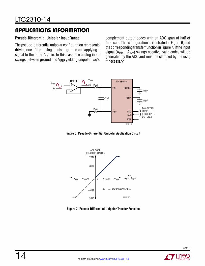
applicaTions inForMaTionPseudo-Differential Unipolar Input Range
The pseudo-differential unipolar configuration represents driving one of the analog inputs at ground and applying a signal to the other AIN pin. In this case, the analog input swings between ground and VREF yielding unipolar two’s
complement output codes with an ADC span of half of full-scale. This configuration is illustrated in Figure 6, and the corresponding transfer function in Figure 7. If the input signal (AIN+ – AIN–) swings negative, valid codes will be generated by the ADC and must be clamped by the user, if necessary.
While single-ended signals can be directly digitized as pre-viously discussed, single-ended to differential conversion circuits may also be used when higher dynamic range is desired. By producing a differential signal at the inputs of the LTC2310-14, the signal swing presented to the ADC is maximized, thus increasing the achievable SNR.
The LT®1819 high speed dual operational amplifier is recommended for performing single-ended-to-differential conversions, as shown in Figure 8. In this case, the first amplifier is configured as a unity-gain buffer and the single-ended input signal directly drives the high imped-ance input of this amplifier.
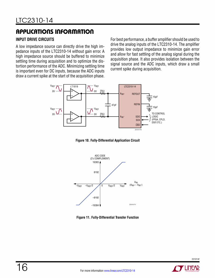
Fully-Differential Inputs
To achieve the best distortion performance of the LTC2310-14, we recommend driving a fully differential signal through LT1819 amplifiers configured as two unity-gain buffers, as shown in Figure 9. This circuit achieves the full data sheet THD specification of –90dB at input frequencies up to 500kHz. A full-differential input signal can span the maximum full-scale of the ADC, up to ±REFOUT. The common mode input voltage can span the entire supply range up to VDD limited by the input signal swing. The fully-differential configuration is illustrated in Figure 10, with the corresponding transfer function illustrated in Figure 11.
Figure 8. Single-Ended to Differential Driver Figure 9. LT1819 Buffering a Fully-Differential Signal Source
A low impedance source can directly drive the high im-pedance inputs of the LTC2310-14 without gain error. A high impedance source should be buffered to minimize settling time during acquisition and to optimize the dis-tortion performance of the ADC. Minimizing settling time is important even for DC inputs, because the ADC inputs draw a current spike at the start of the acquisition phase.
For best performance, a buffer amplifier should be used to drive the analog inputs of the LTC2310-14. The amplifier provides low output impedance to minimize gain error and allow for fast settling of the analog signal during the acquisition phase. It also provides isolation between the signal source and the ADC inputs, which draw a small current spike during acquisition.
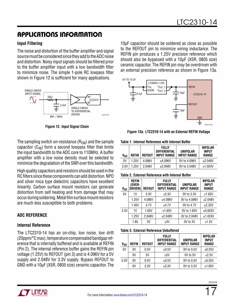
The noise and distortion of the buffer amplifier and signal source must be considered since they add to the ADC noise and distortion. Noisy input signals should be filtered prior to the buffer amplifier input with a low bandwidth filter to minimize noise. The simple 1-pole RC lowpass filter shown in Figure 12 is sufficient for many applications.
10µF capacitor should be soldered as close as possible to the REFOUT pin to minimize wiring inductance. The REFIN pin produces a 1.25V precision reference which should also be bypassed with a 10μF (X5R, 0805 size) ceramic capacitor. The REFIN pin may be overdriven with an external precision reference as shown in Figure 13a.
Figure 12. Input Signal Chain
50Ω
SINGLE-ENDEDINPUT SIGNAL
231014 F12BW = 1MHz
3.3nFSINGLE-ENDEDTO DIFFERENTIALDRIVER
IN+
IN–LTC2310
The sampling switch on-resistance (RON) and the sample capacitor (CIN) form a second lowpass filter that limits the input bandwidth to the ADC core to 110MHz. A buffer amplifier with a low noise density must be selected to minimize the degradation of the SNR over this bandwidth.
High quality capacitors and resistors should be used in the RC filters since these components can add distortion. NPO and silver mica type dielectric capacitors have excellent linearity. Carbon surface mount resistors can generate distortion from self heating and from damage that may occur during soldering. Metal film surface mount resistors are much less susceptible to both problems.
ADC REFERENCE
Internal Reference
The LTC2310-14 has an on-chip, low noise, low drift (20ppm/°C max), temperature compensated bandgap ref-erence that is internally buffered and is available at REFIN (Pin 2). The internal reference buffer gains the REFIN pin voltage (1.25V) to REFOUT (pin 3) and is 4.096V for a 5V supply and 2.048V for 3.3V supply. Bypass REFOUT to GND with a 10μF (X5R, 0805 size) ceramic capacitor. The
Figure 13a. LTC2310-14 with an External REFIN Voltage
The internal reference buffer can also be overdriven from 1.25V to 5V with an external reference at REFOUT as shown in Figure 13b. In this configuration, REFIN must be grounded to disable the internal reference buffer. A 55kΩ internal resistance loads the REFOUT pin when the reference buffer is disabled. To maximize the input signal swing and corresponding SNR, the LTC6655-5 is recommended when overdriving REFOUT. The LTC6655-5 offers the same small size, accuracy, drift and extended temperature range as the LTC6655-4.096. By using a 5V reference, a higher SNR can be achieved. We recommend bypassing the LTC6655-5 with a 10μF ceramic capacitor (X5R, 0805 size) as close as possible to the REFOUT pin.
since any deviation in the voltage at REFOUT will affect the accuracy of the output code. If an external reference is used to buffer/drive the REFOUT pin, the fast settling LTC6655 reference is recommended.
Figure 13b. LTC2310-14 with an External REFOUT Voltage
VINSHDN
VOUT_FVOUT_S
LTC6655-4.096
LTC2310-14
GND
231014 F13b
5V TO 13.2V
REFOUT
REFIN
0.1µF 10µF
Internal Reference Buffer Transient Response
The REFOUT pin of the LTC2310-14 draws charge (QCONV) from the external bypass capacitors during each conver-sion cycle. If the internal reference buffer is overdriven, the external reference must provide all of this charge with a DC current equivalent to IREFOUT = QCONV/tCYC. Thus, the DC current draw of REFOUT depends on the sampling rate and output code. In applications where a burst of samples is taken after idling for long periods, as shown in Figure 14 , IREFOUT quickly goes from approxi-mately ~75µA to a maximum of 350µA for REFOUT = 5V at 2Msps. This step in DC current draw triggers a transient response in the external reference that must be considered
Figure 14. CNV Waveform Showing Burst Sampling
Figure 15. Transient Response of the LTC2310-14
CNV
231014 F14
IDLEPERIOD
231014 F15TIME (ns)
OUTP
UT C
ODE
0 200100
17500
15000
12500
10000
7500
5000
2500
0
–2500
DYNAMIC PERFORMANCE
Fast Fourier transform (FFT) techniques are used to test the ADC’s frequency response, distortion and noise at the rated throughput. By applying a low distortion sine wave and analyzing the digital output using an FFT algorithm, the ADC’s spectral content can be examined for frequen-cies outside the fundamental. The LTC2310-14 provides guaranteed tested limits for both AC distortion and noise measurements.
Signal-to-Noise and Distortion Ratio (SINAD)
The signal-to-noise and distortion ratio (SINAD) is the ratio between the RMS amplitude of the fundamental input frequency and the RMS amplitude of all other frequency components at the A/D output. The output is bandlimited to frequencies from above DC and below half the sampling
applicaTions inForMaTionfrequency. Figure 16 shows that the LTC2310-14 achieves a typical SINAD of 81.7dB at a 2MHz sampling rate with a 500kHz input.
POWER CONSIDERATIONS
The LTC2310-14 requires two power supplies: the 5V power supply (VDD), and the digital input/output interface power supply (OVDD). The flexible OVDD supply allows the LTC2310-14 to communicate with any digital logic operating between 1.8V and 2.5V. When using LVDS I/O, the OVDD supply must be set to 2.5V.
Power Supply Sequencing
The LTC2310-14 does not have any specific power supply sequencing requirements. Care should be taken to adhere to the maximum voltage relationships described in the Absolute Maximum Ratings section. The LTC2310-14 has a power-on-reset (POR) circuit that will reset the LTC2310-14 at initial power-up or whenever the power supply voltage drops below 2V. Once the supply voltage re-enters the nominal supply voltage range, the POR will reinitialize the ADC. No conversions should be initiated until 10ms after a POR event to ensure the reinitialization period has ended. Any conversions initiated before this time will produce invalid results.
Figure 16. 32k Point FFT of the LTC2310-14
SNR = 82dBTHD = –93dBSINAD = 81.7dBSFDR = 97dB
FREQUENCY (MHz)0 0.2 0.4 0.6 0.8 1.0
–140
–120
–100
–80
–60
–40
–20
0
AMPL
ITUD
E (d
BFS)
231014 F16
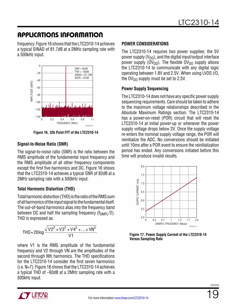
Figure 17. Power Supply Current of the LTC2310-14 Versus Sampling Rate
Signal-to-Noise Ratio (SNR)
The signal-to-noise ratio (SNR) is the ratio between the RMS amplitude of the fundamental input frequency and the RMS amplitude of all other frequency components except the first five harmonics and DC. Figure 16 shows that the LTC2310-14 achieves a typical SNR of 82dB at a 2MHz sampling rate with a 500kHz input.
Total Harmonic Distortion (THD)
Total harmonic distortion (THD) is the ratio of the RMS sum of all harmonics of the input signal to the fundamental itself. The out-of-band harmonics alias into the frequency band between DC and half the sampling frequency (fSMPL/2). THD is expressed as:
THD=20log
V22 + V32 + V42 +…+ VN2
V1
where V1 is the RMS amplitude of the fundamental frequency and V2 through VN are the amplitudes of the second through Nth harmonics. The THD specifications for the LTC2310-14 consider the first seven harmonics (i.e. N=7). Figure 16 shows that the LTC2310-14 achieves a typical THD of –93dB at a 2MHz sampling rate with a 500kHz input.
The LTC2310-14 conversion is controlled by CNV. A falling edge on CNV will start the conversion process. The conversion process is internally timed. For optimum performance, CNV should be driven by a clean low jitter signal. The Typical Application at the back of the data sheet illustrates a recommended implementation to reduce the relatively large jitter from an FPGA CNV pulse source. Note the low jitter input clock times the falling edge of the CNV signal. The rising edge jitter of CNV is much less critical to performance. The minimum pulse width of the CNV signal is 30ns at a 2Msps conversion rate.
SCK Serial Data Clock Input
The falling edge of this clock shifts the conversion result MSB first onto the SDO pins. A 64MHz external clock must be applied at the SCK pin to achieve 2Msps throughput.
Nap/Sleep Modes
Nap mode is a method to save power without sacrificing power-up delays for subsequent conversions. Sleep mode has substantial power savings, but a power-up delay is incurred to allow the reference and power systems to
become valid. To enter nap mode on the LTC2310-14, the SCK signal must be held high or low and a series of two CNV pulses must be applied. This is the case for both CMOS and LVDS modes. The second rising edge of CNV initiates the nap state. The nap state will persist until either a single rising edge of SCK is applied, or further CNV pulses are applied. The SCK rising edge will put the LTC2310-14 back into the operational (full-power) state. When in nap mode, two additional pulses will put the LTC2310-14 in sleep mode. When configured for CMOS I/O operation, a single rising edge of SCK can return the LTC2310-14 into operational mode. A 10ms delay is necessary after exiting sleep mode to allow the reference buffer to recharge the external filter capacitor. In LVDS mode, exit sleep mode by supplying a fifth CNV pulse. The fifth pulse will return the LTC2310-14 to operational mode, and further SCK pulses will keep the part from re-entering nap and sleep modes. The fifth SCK pulse also works in CMOS mode as a method to exit sleep. In the absence of SCK pulses, repetitive CNV pulses will cycle the LTC2310-14 between operational, nap and sleep modes indefinitely.
Refer to the timing diagrams in Figure 18, Figure 19, Figure 20 and Figure 21 for more detailed timing information about sleep and nap modes.
Figure 18. CMOS and LVDS Mode NAP and WAKE Using SCK
The LTC2310-14 features a serial digital interface that is simple and straightforward to use. The flexible OVDD supply allows the LTC2310-14 to communicate with any digital logic operating between 1.8V and 2.5V. A 64MHz external clock must be applied at the SCK pin to achieve 2Msps throughput.
In addition to a standard CMOS SPI interface, the LTC2310-14 provides an optional LVDS SPI interface to support low noise digital design. The CMOS/LVDS pin is used to select the digital interface mode.
The falling edge of SCK outputs the conversion result MSB first on the SDO pins. In CMOS mode, use the SDO+ pin as the serial data output and the SCK+ pin as the serial clock input. Do not connect the SDO– and SCK– pins as they have internal pull-downs to GND.
In LVDS mode, use the SDO+/SDO– pins as a differential output. These pins must be differentially terminated by an external 100Ω resistor at the receiver (FPGA). The SCK+/SCK– pins are a differential input and must be terminated differentially by an external 100Ω resistor at the receiver (ADC), see Figure 22.
BOARD LAYOUT
To obtain the best performance from the LTC2310-14, a four layer printed circuit board is recommended. Layout for the printed circuit board (PCB) should ensure the digital and analog signal lines are separated as much as possible. In particular, care should be taken not to run any digital clocks or signals adjacent to analog signals or underneath the ADC.
A single solid ground plane is used. Bypass capacitors to the supplies are placed as close as possible to the supply pins. Low impedance common returns for these bypass capacitors are essential to the low noise operation of the ADC. The analog input traces are screened by ground.
Reference Design
For a detailed look at the reference design for this converter, including schematics and PCB layout, please refer to the DC2425, the evaluation kit for the LTC2310-14.
Information furnished by Linear Technology Corporation is believed to be accurate and reliable. However, no responsibility is assumed for its use. Linear Technology Corporation makes no representa-tion that the interconnection of its circuits as described herein will not infringe on existing patent rights.
package DescripTionPlease refer to http://www.linear.com/product/LTC2310-14#packaging for the most recent package drawings.
MSOP (MSE16) 0213 REV F
0.53 ±0.152(.021 ±.006)
SEATINGPLANE
0.18(.007)
1.10(.043)MAX
0.17 – 0.27(.007 – .011)
TYP
0.86(.034)REF
0.50(.0197)
BSC
16
16151413121110
1 2 3 4 5 6 7 8
9
9
1 8
NOTE:1. DIMENSIONS IN MILLIMETER/(INCH)2. DRAWING NOT TO SCALE3. DIMENSION DOES NOT INCLUDE MOLD FLASH, PROTRUSIONS OR GATE BURRS. MOLD FLASH, PROTRUSIONS OR GATE BURRS SHALL NOT EXCEED 0.152mm (.006") PER SIDE4. DIMENSION DOES NOT INCLUDE INTERLEAD FLASH OR PROTRUSIONS. INTERLEAD FLASH OR PROTRUSIONS SHALL NOT EXCEED 0.152mm (.006") PER SIDE5. LEAD COPLANARITY (BOTTOM OF LEADS AFTER FORMING) SHALL BE 0.102mm (.004") MAX6. EXPOSED PAD DIMENSION DOES INCLUDE MOLD FLASH. MOLD FLASH ON E-PAD SHALL NOT EXCEED 0.254mm (.010") PER SIDE.