LTC3212 3212fb TYPICAL APPLICATION FEATURES APPLICATIONS DESCRIPTION RGB LED Driver and Charge Pump The LTC ® 3212 is a low noise charge pump RGB LED driver capable of driving three LEDs up to 25mA each from a 2.7V to 5.5V input. Low external part count (one flying capacitor, two bypass capacitors and one to three programming resistors) makes the LTC3212 ideally suited for small, battery-powered applications. Built-in soft-start circuitry prevents excessive inrush cur- rent during start-up and mode switching. High switching frequency enables the use of small external capacitors. The charge pump shuts down to a high impedance mode to prevent LED leakage while the LTC3212 is off. Each LED may be individually turned on or off via a single pin interface. The current through the LEDs may be indi- vidually programmed with resistors or may share a single programming resistor. White mode adjusts the red, green and blue LED current ratios for a white light when all three LEDs are programmed to be on. LED currents are regulated using internal low dropout current sources. Automatic mode switching optimizes efficiency by monitoring the LED current drivers and switches mode only when dropout is detected. The part is available in a 3mm × 2mm 12-lead DFN package. RGB Power Supply and Current Control ■ Power and Current Control for Driving RGB LEDs ■ Individually Programmable Current Sources ■ 1x or 2x Mode, Low Noise, Constant Frequency Charge Pump ■ Single Wire Enable Control for All LEDs ■ White Mode Adjusts R, G, B Currents for White Light ■ 25mA Maximum LED Current ■ V IN Range: 2.7V to 5.5V ■ Automatic Soft-Start, Mode Switching and Output Disconnect in Shutdown Mode ■ Available in 12-Lead (3mm × 2mm) DFN Package ■ Cellular Phones ■ Media Players ■ RGB Back Lights , LT, LTC and LTM are registered trademarks of Linear Technology Corporation. All other trademarks are the property of their respective owners. Protected by U.S. Patents, including 6411531. LEDR CPO CM CP V IN LEDEN 1µF 1µF LTC3212 1µF R G B 3212 TA01a 11.8k V IN 2.7V TO 5.5V I SETB I SETR I SETG LEDG LEDB INDIVIDUAL SETTINGS 15mA 15mA 15mA LEDR LEDG LEDB WHITE MODE 13.5mA 15mA 11.2mA
Transcript
LTC3212
3212fb
Typical applicaTion
FeaTures
applicaTions
DescripTion
RGB LED Driver and Charge Pump
The LTC®3212 is a low noise charge pump RGB LED driver capable of driving three LEDs up to 25mA each from a 2.7V to 5.5V input. Low external part count (one flying capacitor, two bypass capacitors and one to three programming resistors) makes the LTC3212 ideally suited for small, battery-powered applications.
Built-in soft-start circuitry prevents excessive inrush cur-rent during start-up and mode switching. High switching frequency enables the use of small external capacitors. The charge pump shuts down to a high impedance mode to prevent LED leakage while the LTC3212 is off.
Each LED may be individually turned on or off via a single pin interface. The current through the LEDs may be indi-vidually programmed with resistors or may share a single programming resistor. White mode adjusts the red, green and blue LED current ratios for a white light when all three LEDs are programmed to be on.
LED currents are regulated using internal low dropout current sources. Automatic mode switching optimizes efficiency by monitoring the LED current drivers and switches mode only when dropout is detected. The part is available in a 3mm × 2mm 12-lead DFN package.
RGB Power Supply and Current Control
Power and Current Control for Driving RGB LEDs Individually Programmable Current Sources 1x or 2x Mode, Low Noise, Constant Frequency
Charge Pump Single Wire Enable Control for All LEDs White Mode Adjusts R, G, B Currents for White Light 25mA Maximum LED Current VIN Range: 2.7V to 5.5V Automatic Soft-Start, Mode Switching and Output
Disconnect in Shutdown Mode Available in 12-Lead (3mm × 2mm) DFN Package
Cellular Phones Media Players RGB Back Lights , LT, LTC and LTM are registered trademarks of Linear Technology Corporation.All other trademarks are the property of their respective owners.Protected by U.S. Patents, including 6411531.
LEDR
CPO
CM CP
VIN
LEDEN
1µF
1µF
LTC3212 1µFR G B
3212 TA01a
11.8k
VIN2.7V TO 5.5V
ISETBISETRISETG
LEDG
LEDB
INDIVIDUALSETTINGS
15mA15mA15mA
LEDRLEDGLEDB
WHITEMODE
13.5mA15mA
11.2mA
LTC3212
3212fb
pin conFiGuraTionabsoluTe MaxiMuM raTinGsVIN to GND ................................................... –0.3V to 6VCPO to GND ................................................. –0.3V to 6VLEDEN ............................................. –0.3V to VIN + 0.3VICPO (Note 2) ..........................................................75mAILED(R,G,B) (Note 2) .................................................30mACPO Short-Circuit Duration .............................. IndefiniteOperating Temperature Range
(Notes 3, 4) .......................................... –40°C to 85°CStorage Temperature Range ................... –65°C to 125°C
(Note 1)TOP VIEW
13
DDB PACKAGE12-LEAD (3mm × 2mm) PLASTIC DFN
CP
CPO
LEDEN
ISETB
ISETR
ISETG
VIN
CM
GND
LEDB
LEDR
LEDG
8
7
10
9
11
12
5
6
4
2
3
1
TJMAX = 125°C, θJA = 76°C/W
EXPOSED PAD (PIN 13) IS GND, MUST BE SOLDERED TO PCB
Consult LTC Marketing for parts specified with wider operating temperature ranges. Consult LTC Marketing for information on non-standard lead based finish parts.For more information on lead free part marking, go to: http://www.linear.com/leadfree/ For more information on tape and reel specifications, go to: http://www.linear.com/tapeandreel/
LTC3212
3212fb
elecTrical characTerisTics
Note 1: Stresses beyond those listed under Absolute Maximum Ratings may cause permanent damage to the device. Exposure to any Absolute Maximum Rating condition for extended periods may affect device reliability and lifetime.Note 2: Based on long-term current density limitations. Note 3: The LTC3212E is guaranteed to meet performance specifications from 0°C to 85°C. Specifications over the –40°C to 85°C ambient operating temperature range are assured by design, characterization and correlation with statistical process controls
The denotes the specifications which apply over the full operating temperature range, otherwise specifications are at TA = 25°C. VIN = 3.6V.
PARAMETER CONDITIONS MIN TYP MAX UNITS
2x Mode Output Impedance (Notes 6, 7) 25 Ω
CLK Frequency 650 900 1275 kHz
LEDEN
High Level Input Voltage (VIH) 1.4 V
Low Level Input Voltage (VIL) 0.4 V
Input Current (IIH) LEDEN = 3.6V 3 10 µA
Input Current (IIL) –1 1 µA
tPWH High Pulse Width 0.08 µs
tPWL Low Pulse Width 0.08 20 µs
tSD Low Time to Shutdown (LEDEN = Low) 350 µs
ISET(R,G,B)
VISET 864 925 985 mV
IISET 140 µA
Note 4: This IC includes overtemperature protection that is intended to protect the device during momentary overload conditions. Junction temperature will exceed 125°C when overtemperature protection is active. Continuous operation above the specified maximum operating junction temperature may impair device reliability.Note 5: If the LTC3212 has been shut down, then the initial enable time is longer due to the bandgap settling time and the CPO output capacitor soft-start time.Note 6: 1x mode output impedance is defined as (VIN – VCPO)/IOUT. 2x mode output impedance is defined as (2VIN – VCPO)/IOUT.Note 7: Guaranteed by design.
Typical perForMance characTerisTics
Dropout Time 2x Mode CPO RippleLED Pin Dropout Voltage vs LED Pin Current
CPO1V/DIV
LED500mV/DIV
50µs/DIV 3212 G01
2x MODE1x MODE3.6V 5.1V
0V
1V
DROPOUT
DROPOUTDELAY
LED CURRENT (mA)0
LED
DROP
OUT
VOLT
AGE
(mV)
100
150
20
3212 G03
50
05 10 15
250
200
500ns/DIVVIN = 3.6VICPO = 75mACCPO = 1µF
3212 G02
VCPO20mV/DIV
AC COUPLED
LTC3212
3212fb
Typical perForMance characTerisTics
1x Mode Charge Pump Resistance vs Temperature
2x Mode CPO Open-Loop Output Resistance
2x Mode CPO Voltage vs CPO Current
Oscillator Frequency vs VIN Voltage
VIN Shutdown Current vs VIN Voltage
1x Mode No-Load VIN Current vs VIN Voltage
2x Mode VIN Current vs VIN Voltage
VIN (V)2.7
OPEN
-LOO
P OU
TPUT
RES
ISTA
NCE
(Ω)
27
31
3.6
3212 G05
23
19
25
29
33
35
21
17
153.0 3.3 4.0
85°C
C1, C2, C3 = 1µFVCPO = 4.8V
25°C
–40°C
CPO CURRENT (mA)0
4.0
CPO
VOLT
AGE
(V)
4.2
4.4
4.6
4.8
5.2
20 30 40 50
3212 G06
6010 25 35 45 55 65 70
5.0
3.6V
3.1V
3.2V3.3V3.4V
VIN = 3.0V
C1, C2, C3 = 1µF
3.5V
VIN (V)2.7
FREQ
UENC
Y (k
Hz)
888
890
892
3.9 4.7
3212 G07
886
884
3.1 3.5 4.3 5.1 5.5
882
880
VIN (V)2.7
0
I VIN
(µA)
1
2
3
4
6
3.53.1 3.9 4.3 4.7 5.1
3212 G08
5.5
5
VIN (V)2.7
290
V IN
CURR
ENT
(µA)
300
310
320
330
350
3.1 3.5 3.9 4.3
3212 G09
5.14.7 5.5
340
Start-Up and Mode Switch
VIN (V)2.7
V IN
CURR
ENT
(mA)
3.5
3.9
3212 G10
2.0
1.0
3.1 3.5 4.3
0.5
0
4.0
3.0
2.5
1.5
4.7 5.1 5.5
CPO1V/DIV
LEDEN2V/DIV
200µs/DIVVIN = 3.6V 3212 G11
SOFT-START
DROPOUTDELAY1x
MODE
2xMODE
0V
0V
3.6V
3.6V
5V
TEMPERATURE (°C)–40
5.0
5.5
6.5
20 60
3212 G04
4.5
4.0
–20 0 40 80
3.5
3.0
6.0
RESI
STAN
CE (Ω
)
VIN = 3V
ICPO = 50mA
VIN = 3.6V
VIN = 4.2V
LTC3212
3212fb
pin FuncTionsCP, CM (Pins 1, 11): Charge Pump Flying Capacitor Pins. A 1µF X5R or X7R ceramic capacitor should be connected from CP to CM.
CPO (Pin 2): CPO is the output of the charge pump. A 1µF X5R or X7R ceramic capacitor is required from CPO to GND. While operating, this pin will supply current to the LEDs and while in shutdown mode this pin will be high impedance.
LEDEN (Pin 3): The LEDEN pin is used to program, enable and shut down the part. A 3µA internal current source pulls this pin to ground.
ISETB, ISETR, ISETG (Pins 4, 5, 6): LED current program-ming resistor pins. A resistor connected between a pin and GND is used to set the LED current. A resistor from ISETG to GND is required. Resistors on ISETR and ISETB are optional. If ISETR and/or ISETB is not connected to a resistor ISETR’s and/or ISETB’s respective output(s) will be
automatically programmed by the resistor connected to ISETG. If ISETR or ISETB is unused the pin should be con-nected to VIN.
LEDG, LEDR, LEDB (Pins 7, 8, 9): These pins are the LED current output pins. The LEDs are connected from either the charge pump or VIN (anode) to LED (R, G, B) (cathode).
GND (Pin 10): This pin should be connected directly to a low impedance ground plane.
VIN (Pin 12): Supply voltage for the LTC3212. VIN should be bypassed with a low impedance ceramic capacitor to GND of at least 1µF of capacitance.
Exposed Pad (Pin 13): GND. The Exposed Pad must be soldered to a low impedance ground plane for optimum performance.
LTC3212
3212fb
block DiaGraM
4
+–
LEDCURRENTSOURCE
ENBLEDB
LEDR
LEDG
3212 BD
ISETB
ENR ENG ENB
3LEDEN
3µA
12VIN
5
+–
LEDCURRENTSOURCE
ENR
ISETR
6
+–
LEDCURRENTSOURCE
OPENDETECTION/
AUTOSET
ENG
ISETG
10GND
CONTROL LOGIC DROPOUTDETECTION
VREF
CP
TSD
9
8
7
10k
SHUTDOWN
CPO2
1
CM
11
–
+
900kHzOSCILLATOR
The LTC3212 uses a switched capacitor charge pump to power three LEDs with a programmable regulated cur-rent. The part powers up into 1x mode. In this mode VIN is directly connected to CPO. When powering up into 1x mode, the LTC3212 charges the CPO capacitor to near VIN before directly connecting VIN to CPO. This prevents a large in-rush current. 1x mode provides maximum ef-ficiency and minimum noise. The LTC3212 will remain in this mode until one of the LED current source drivers
operaTionbegins to drop out of regulation. When this drop out oc-curs the LTC3212 will switch to 2x mode after a soft-start period. The part will return to 1x mode when the part is shut down and reprogrammed.
The current delivered through the LED load is controlled by an internal programmable low dropout current source. The current is programmed by resistors connected between the ISET(R,G,B) pins and GND.
LTC3212
3212fb
operaTionAn overcurrent shutdown mode on the ISET pins will pre-vent damage to the part and the LED by shutting down the LED drivers. Choosing an RSET value of 5.9k or greater will ensure that the part stays out of this mode. When in normal operating mode current, regulation is achieved by controlling an active current source.
In shutdown mode all internal circuitry is turned off and the LTC3212 draws very little current from the VIN supply. The LTC3212 enters shutdown mode after the LEDEN pin is brought low for 350µs.
Short-Circuit Protection
When LEDEN is brought high, the part will connect VIN to CPO through a weak pull-up until CPO has charged to near VIN. After the LTC3212 detects that the CPO voltage is near the VIN voltage, it then enables 1x mode. If the CPO is shorted or falls below approximately 1V, then the LTC3212 is disabled. After falling below 1V the LTC3212 will use the weak pull-up to charge CPO to near VIN before re-enabling the chip.
Soft-Start
To prevent excessive inrush during start-up and mode switching, the LTC3212 employs built-in soft-start circuitry. Soft-start is achieved by increasing the current available to the CPO capacitor over a period of approximately 100µs.
Charge Pump Strength
When the LTC3212 operates in 2x mode, the charge pump can be modeled as a Thevenin equivalent circuit to determine the amount of current available from the effective input voltage and the effective open-loop output resistance, ROL.
+
–
+–
ROL
CPO2VIN
3212 F01
Figure 1. CPO Equivalent Open-Loop
ROL is dependent on a number of factors including the oscillator frequency, flying capacitor values and switch resistances. From Figure 1 we can see that the maximum output current in 2x mode is proportional to:
2V CPOR
IN
OL
–
LED Current Programming
The LTC3212 includes three accurate, programmable cur-rent sources that are capable of driving LED currents up to 25mA continuously. The current is programmed using an external resistor for each channel. The equation for each external resistance is:
RI
RI
R
SETGLEDG
SETBLEDB
SETR
=
=
=
177 6
177 6
177 6
.
.
.IILEDR
Alternatively, if either the ISETR or ISETB pins are connected to VIN, the respective LEDR and/or LEDB current will au-tomatically use the RSETG resistor and be set to:
IR
IR
LEDRSETG
LEDBSETG
=
=
177 6
177 6
.
.
LTC3212
3212fb
White Mode
The LTC3212 has a white mode that automatically scales the current in the red, green and blue LEDs to a preset mix when selected. This allows the currents programmed with the external resistors to be set independently of the ratio needed for white light, increasing the flexibility of program-ming other colors. The intensity of the white is set by the resistor on ISETG. The ratio used for white mode is:
IR
IR
I
LEDGSETG
LEDRSETG
LEDB
=
=
=
177 6
159 8
133 2
.
.
.RRSETG
Enable
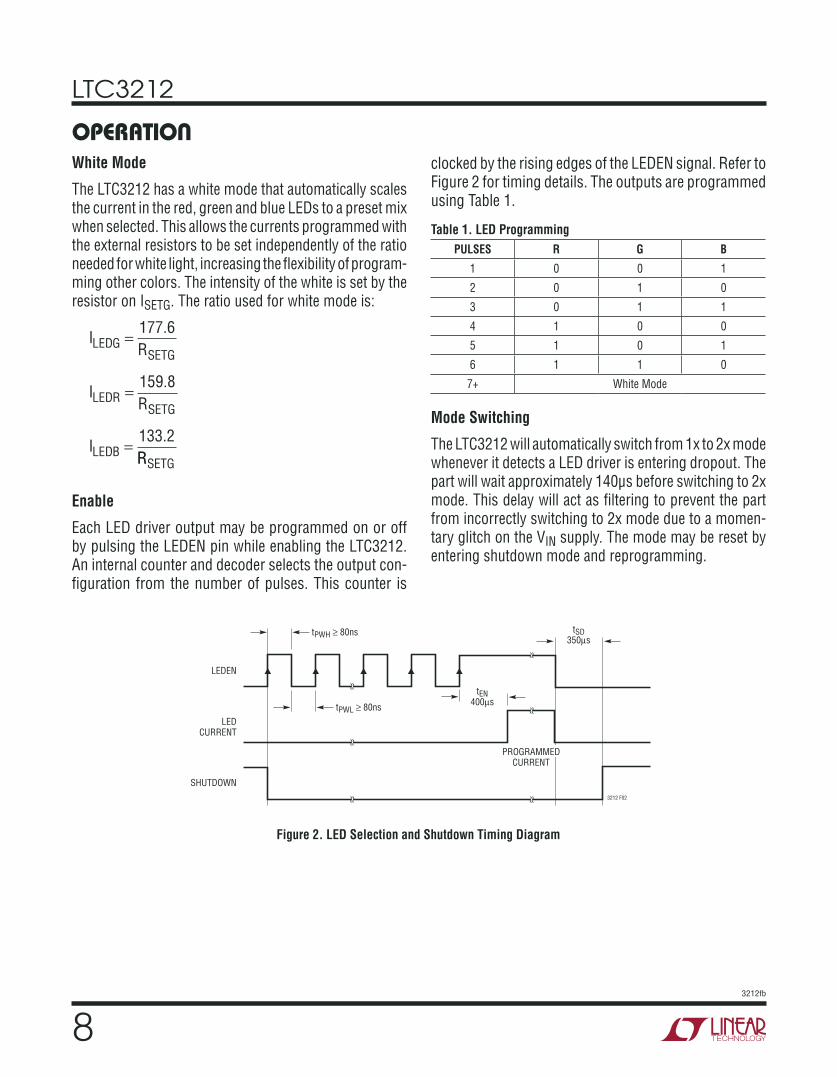
Each LED driver output may be programmed on or off by pulsing the LEDEN pin while enabling the LTC3212. An internal counter and decoder selects the output con-figuration from the number of pulses. This counter is
operaTionclocked by the rising edges of the LEDEN signal. Refer to Figure 2 for timing details. The outputs are programmed using Table 1.
Table 1. LED ProgrammingPULSES R G B
1 0 0 1
2 0 1 0
3 0 1 1
4 1 0 0
5 1 0 1
6 1 1 0
7+ White Mode
Mode Switching
The LTC3212 will automatically switch from 1x to 2x mode whenever it detects a LED driver is entering dropout. The part will wait approximately 140µs before switching to 2x mode. This delay will act as filtering to prevent the part from incorrectly switching to 2x mode due to a momen-tary glitch on the VIN supply. The mode may be reset by entering shutdown mode and reprogramming.
LEDEN
SHUTDOWN
LEDCURRENT
tPWH ≥ 80ns
tPWL ≥ 80ns
tEN400µs
tSD350µs
PROGRAMMEDCURRENT
3212 F02
Figure 2. LED Selection and Shutdown Timing Diagram
The style and value of the capacitors used with the LTC3212 determine several important parameters such as regulator control loop stability, output ripple, charge pump strength and minimum start-up time.
To reduce noise and ripple, it is recommended that low equivalent series resistance (ESR) ceramic capacitors are used for both CVIN and CCPO. Tantalum and aluminum capacitors are not recommended due to high ESR.
The value of CCPO directly controls the amount of output ripple for a given load current. Increasing the size of CCPO will reduce output ripple at the expense of longer start-up time. The peak-to-peak output ripple of the 2x mode is approximately given by the expression:
VRIPPLEP-P =
If C
OUT
OSC CPO2 •
where fOSC is the LTC3212 oscillator frequency or typically 900kHz and CCPO is the output storage capacitor.
Flying Capacitor Selection
Warning: Polarized capacitors such as tantalum or aluminum should never be used for the flying capaci-tors since their voltage can reverse upon start-up of the LTC3212. Ceramic capacitors should always be used for the flying capacitors.
The flying capacitors control the strength of the charge pump. In order to achieve the rated output current it is necessary to have at least 0.6µF of capacitance for flying capacitor. Capacitors of different materials lose their ca-pacitance with higher temperature and voltage at different rates. For example, a ceramic capacitor made of X7R mate-rial will retain most of its capacitance from –40°C to 85°C whereas a Z5U or Y5V style capacitor will lose considerable capacitance over that range. Z5U and Y5V capacitors may also have a very poor voltage coefficient causing them to lose 60% or more of their capacitance when the rated
voltage is applied. Therefore, when comparing different capacitors, it is often more appropriate to compare the amount of achievable capacitance for a given case size rather than comparing the specified capacitance value. For example, over rated voltage and temperature conditions, a 1µF, 10V, Y5V ceramic capacitor in a 0603 case may not provide any more capacitance than a 0.22µF, 10V, X7R available in the same case. The capacitor manufacturer’s data sheet should be consulted to determine what value of capacitor is needed to ensure minimum capacitances at all temperatures and voltages.
Table 2 shows a list of ceramic capacitor manufacturers and how to contact them:
The LTC3212 has been designed to minimize EMI. How-ever due to its high switching frequency and the transient currents produced by the LTC3212, careful board layout is necessary. A true ground plane and short connections to all capacitors will improve performance and ensure proper regulation under all conditions.
The flying capacitor pins CP and CM will have 5ns to 10ns edge rate waveforms. The large dv/dt on these pins can couple energy capacitively to adjacent PCB runs. Magnetic fields can also be generated if the flying capacitors are not close to the LTC3212 (i.e., the loop area is large). To decouple capacitive energy transfer, a Faraday shield may be used. This is a grounded PCB trace between the sensitive node and the LTC3212 pins. For a high quality AC ground, it should be returned to a solid ground plane that extends all the way to the LTC3212.
LTC3212
03212fb
Power Efficiency
To calculate the power efficiency (η) of an LED driver chip, the LED power should be compared to the input power. The difference between these two numbers represents lost power whether it is in the charge pump or the cur-rent sources. Stated mathematically, the power efficiency is given by:
η =
PPLED
IN
The efficiency of the LTC3212 depends upon the mode in which it is operating. Recall that the LTC3212 operates as a pass switch, connecting VIN to CPO, until dropout is detected at an ILED pin. This feature provides the op-timum efficiency available for a given input voltage and LED forward voltage. When it is operating as a switch, the efficiency is approximated by:
η = = =
PP
V IV I
VV
LED
IN
LED LED
BAT BAT
LED
BAT
••
since the input current will be very close to the sum of the LED currents.
At moderate to high output power, the quiescent current of the LTC3212 is negligible and the expression above is valid.
Once dropout is detected at any LED pin, the LTC3212 enables the charge pump in 2x mode.
In 2x boost mode, the efficiency is similar to that of a linear regulator with an effective input voltage of 2 times the actual input voltage. In an ideal 2x charge pump, the power efficiency would be given by:
ηIDEAL
LED
IN
LED LED
BAT LED
LEDPP
V IV I
VV
= = =•
• • •2 2 BBAT
In some applications it may be possible to increase the efficiency of the LTC3212. If any of the LED’s maximum forward voltage is less than the minimum VIN supply volt-age minus ILED dropout voltage then the charge pump is not needed to drive that LED. This is often the case with the red LED due to its lower forward voltage. Its anode may be connected directly to VIN, bypassing the charge pump’s losses in 2x mode.
Thermal Management
If the junction temperature increases above approximately 140°C the thermal shutdown circuitry will automatically deactivate the output current sources and charge pump. To reduce maximum junction temperature, a good thermal connection to the PC board is recommended. Connecting the Exposed Pad to a ground plane and maintaining a solid ground plane under the device will reduce the thermal resistance of the package and PC board considerably.
applicaTions inForMaTion
LTC3212
3212fb
Information furnished by Linear Technology Corporation is believed to be accurate and reliable. However, no responsibility is assumed for its use. Linear Technology Corporation makes no representa-tion that the interconnection of its circuits as described herein will not infringe on existing patent rights.
NOTE:1. DRAWING IS NOT A JEDEC PACKAGE OUTLINE 2. DRAWING NOT TO SCALE 3. ALL DIMENSIONS ARE IN MILLIMETERS4. DIMENSIONS OF EXPOSED PAD ON BOTTOM OF PACKAGE DO NOT INCLUDE MOLD FLASH. MOLD FLASH, IF PRESENT, SHALL NOT EXCEED 0.15mm ON ANY SIDE5. EXPOSED PAD SHALL BE SOLDER PLATED6. SHADED AREA IS ONLY A REFERENCE FOR PIN 1 LOCATION ON THE TOP AND BOTTOM OF PACKAGE
0.40 ± 0.10
BOTTOM VIEW—EXPOSED PAD
0.64 ± 0.10(2 SIDES)
0.75 ±0.05
R = 0.115TYPR = 0.05
TYP
2.39 ±0.10(2 SIDES)
3.00 ±0.10(2 SIDES)
16
127
PIN 1 BARTOP MARK
(SEE NOTE 6)
0.200 REF
0 – 0.05
(DDB12) DFN 0106 REV Ø
0.23 ± 0.050.45 BSC
PIN 1R = 0.20 OR0.25 × 45°CHAMFER
0.25 ± 0.05
2.39 ±0.05(2 SIDES)
RECOMMENDED SOLDER PAD PITCH AND DIMENSIONSAPPLY SOLDER MASK TO AREAS THAT ARE NOT SOLDERED
0.64 ±0.05(2 SIDES)
1.15 ±0.05
0.70 ±0.05
2.55 ±0.05
PACKAGEOUTLINE
0.45 BSC
LTC3212
3212fb
Linear Technology Corporation1630 McCarthy Blvd., Milpitas, CA 95035-7417 (408) 432-1900 FAX: (408) 434-0507 www.linear.com LINEAR TECHNOLOGY CORPORATION 2007
LTC3200-5 Low Noise, 2MHz Regulated Charge Pump White LED Driver
Up to 6 White LEDs, VIN: 2.7V to 4.5V, VOUT(MAX) = 5V, IQ = 8mA, ISD ≤1µA, ThinSOT Package
LTC3201 Low Noise, 1.7MHz Regulated Charge Pump White LED Driver
Up to 6 White LEDs, VIN: 2.7V to 4.5V, VOUT(MAX) = 5V, IQ = 6.5mA, ISD ≤1µA, 10-Lead MS Package
LTC3202 Low Noise, 1.5MHz Regulated Charge Pump White LED Driver
Up to 8 White LEDs, VIN: 2.7V to 4.5V, VOUT(MAX) = 5V, IQ = 5mA, ISD ≤1µA, 10-Lead MS Package
LTC3205 Multidisplay LED Controller 92% Efficiency, VIN: 2.8V to 4.5V, IQ = 50µA, ISD ≤ 1µA, 4mm × 4mm QFN Package
LTC3206 I2C Multidisplay LED Controller 92% Efficiency, 400mA Continuous Output Current; Up to 11 White LEDs in 4mm × 4mm QFN Package
LTC3208 High Current Software Configurable Multidisplay LED Controller
95% Efficiency, VIN: 2.9V to 4.5V, 1A Output Current; Up to 17 LEDs for 5 Displays, 5mm × 5mm QFN Package
LTC3209 600mA MAIN/Camera LED Controller Up to 8 LEDs, 94% Efficiency, VIN: 2.9V to 4.5V, 1x/1.5x/2x Boost Modes, 4mm × 4mm QFN Package
LTC3210/LTC3210-1
500mA MAIN/Camera LED Controller Up to 5 LEDs, 95% Efficiency, VIN: 2.9V to 4.5V, 1x/1.5x/2x Boost Modes, Exponential Brightness Control, “-1” Version Has 64-Step Linear Brightness Control, 3mm × 3mm QFN Package
LTC3210-2 MAIN/CAM LED Controller with 32-Step Brightness Control
Drives 4 MAIN LEDs, 3mm × 3mm QFN Package
LTC3210-3 MAIN/CAM LED Controller with 32-Step Brightness Control
Drives 3 MAIN LEDs, 3mm × 3mm QFN Package
LTC3214 500mA Camera LED Charge Pump 93% Efficiency, VIN: 2.9V to 4.4V, 1x/1.5x/2x Boost Modes, 3mm × 3mm DFN Package
LTC3215 700mA High Current, Low Noise, White LED Driver
LTC3216 1A High Current, Low Noise, White LED Driver 93% Efficiency, VIN: 2.9V to 4.4V, 1x/1.5x/2x Boost Modes, Independent Low/High Current Programming
LTC3217 600mA Low Noise Multi-LED Camera Light Charge Pump
Up to 4 LEDs, 92% Efficiency, VIN: 2.9V to 4.5V, 1x/1.5x/2x Boost Modes, Independent Torch and Flash ISET and Enable Pins, 3mm × 3mm QFN Package
LT3465/LT3465A
1.2MHz/2.4MHz White LED Boost Converters with Internal Schottky
Up to 6 White LEDs, VIN: 12.7V to 16V, VOUT(MAX) = 34V, IQ = 1.9mA, ISD <1µA, ThinSOT Package
ThinSOT is a trademark of Linear Technology Corporation.