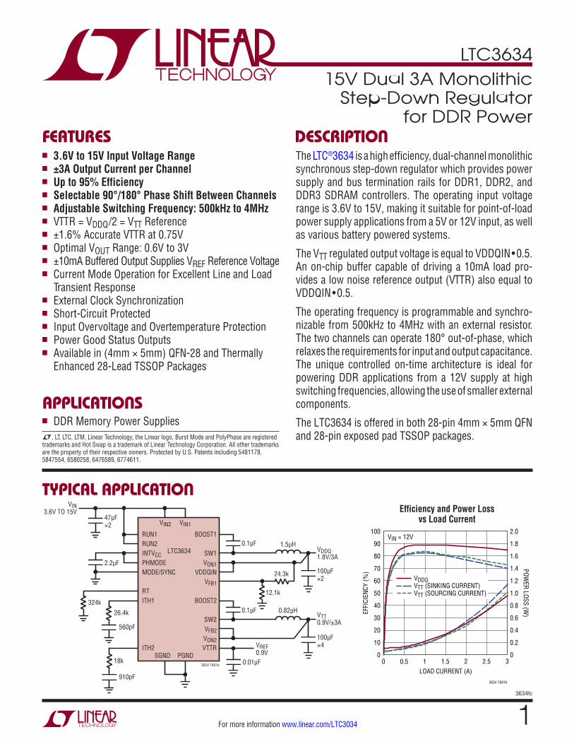
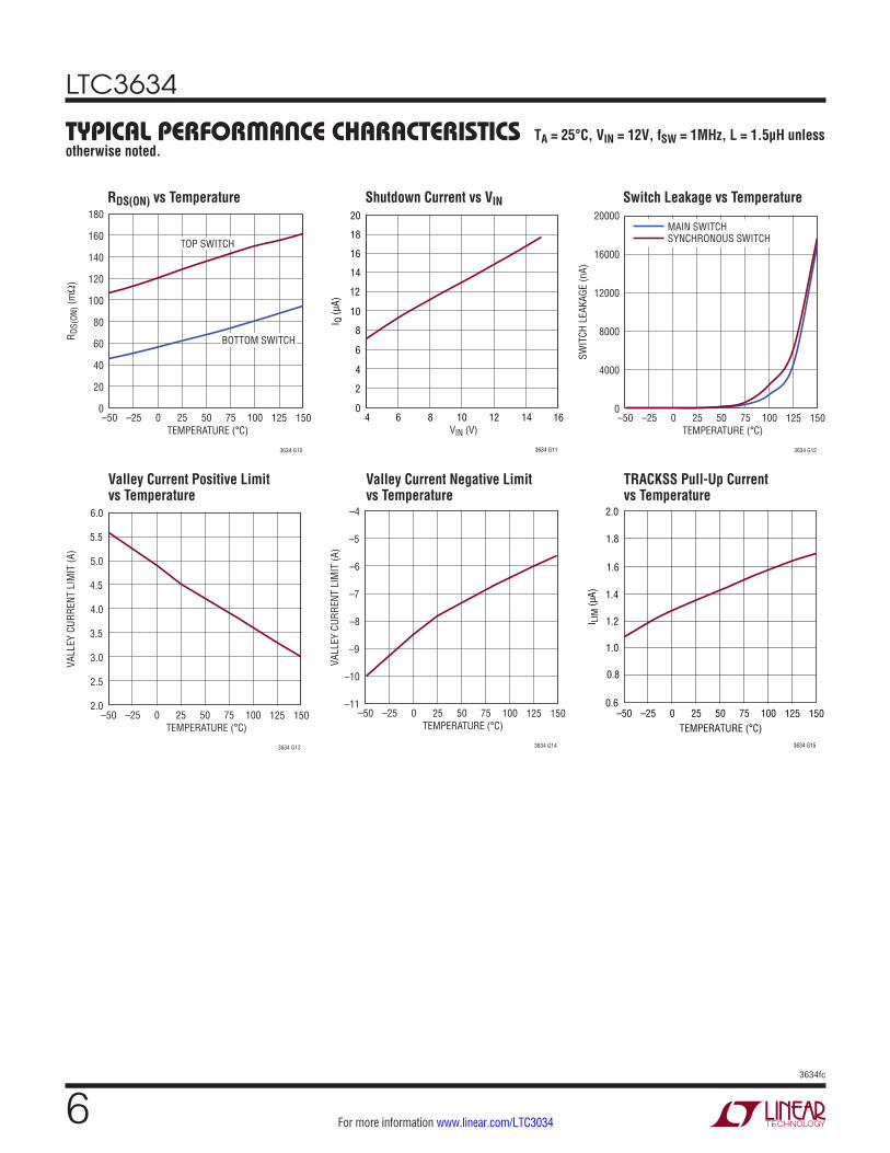
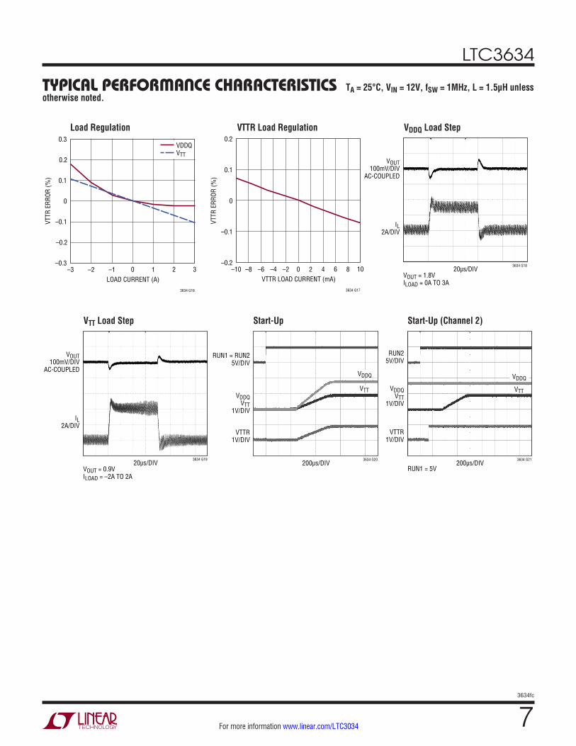
LTC3634 1 3634fc For more information www.linear.com/LTC3034 TYPICAL APPLICATION FEATURES DESCRIPTION 15V Dual 3A Monolithic Step-Down Regulator for DDR Power The LTC ® 3634 is a high efficiency, dual-channel monolithic synchronous step-down regulator which provides power supply and bus termination rails for DDR1, DDR2, and DDR3 SDRAM controllers. The operating input voltage range is 3.6V to 15V, making it suitable for point-of-load power supply applications from a 5V or 12V input, as well as various battery powered systems. The V TT regulated output voltage is equal to VDDQIN • 0.5. An on-chip buffer capable of driving a 10mA load pro- vides a low noise reference output (VTTR) also equal to VDDQIN • 0.5. The operating frequency is programmable and synchro- nizable from 500kHz to 4MHz with an external resistor. The two channels can operate 180° out-of-phase, which relaxes the requirements for input and output capacitance. The unique controlled on-time architecture is ideal for powering DDR applications from a 12V supply at high switching frequencies, allowing the use of smaller external components. The LTC3634 is offered in both 28-pin 4mm × 5mm QFN and 28-pin exposed pad TSSOP packages. Efficiency and Power Loss vs Load Current APPLICATIONS n 3.6V to 15V Input Voltage Range n ±3A Output Current per Channel n Up to 95% Efficiency n Selectable 90°/180° Phase Shift Between Channels n Adjustable Switching Frequency: 500kHz to 4MHz n VTTR = V DDQ /2 = V TT Reference n ±1.6% Accurate VTTR at 0.75V n Optimal V OUT Range: 0.6V to 3V n ±10mA Buffered Output Supplies V REF Reference Voltage n Current Mode Operation for Excellent Line and Load Transient Response n External Clock Synchronization n Short-Circuit Protected n Input Overvoltage and Overtemperature Protection n Power Good Status Outputs n Available in (4mm × 5mm) QFN-28 and Thermally Enhanced 28-Lead TSSOP Packages n DDR Memory Power Supplies RUN1 RUN2 INTV CC PHMODE MODE/SYNC RT ITH1 ITH2 LTC3634 3634 TA01a 1.5μH 24.3k 12.1k 0.1μF 0.01μF V REF 0.9V 0.1μF PGND SGND BOOST1 SW1 V ON1 VDDQIN V FB1 BOOST2 SW2 V FB2 V ON2 VTTR V IN1 V IN 3.6V TO 15V V IN2 0.82μH 18k 100μF ×2 V DDQ 1.8V/3A 100μF ×4 V TT 0.9V/±3A 910pF 26.4k 324k 560pF 2.2μF 47μF ×2 L, LT, LTC, LTM, Linear Technology, the Linear logo, Burst Mode and PolyPhase are registered trademarks and Hot Swap is a trademark of Linear Technology Corporation. All other trademarks are the property of their respective owners. Protected by U.S. Patents including 5481178, 5847554, 6580258, 6476589, 6774611. LOAD CURRENT (A) 0 70 80 100 1.5 2.5 3634 TA01b 30 20 0.5 1 2 3 10 60 50 40 0 90 1.4 1.6 2.0 0.6 0.4 0.2 1.2 1.0 0.8 0 1.8 EFFICIENCY (%) POWER LOSS (W) V IN = 12V V DDQ V TT (SINKING CURRENT) V TT (SOURCING CURRENT)
Transcript
LTC3634
13634fc
For more information www.linear.com/LTC3034
TYPICAL APPLICATION
FEATURES DESCRIPTION
15V Dual 3A Monolithic Step-Down Regulator
for DDR Power
The LTC®3634 is a high efficiency, dual-channel monolithic synchronous step-down regulator which provides power supply and bus termination rails for DDR1, DDR2, and DDR3 SDRAM controllers. The operating input voltage range is 3.6V to 15V, making it suitable for point-of-load power supply applications from a 5V or 12V input, as well as various battery powered systems.
The VTT regulated output voltage is equal to VDDQIN•0.5. An on-chip buffer capable of driving a 10mA load pro-vides a low noise reference output (VTTR) also equal to VDDQIN•0.5.
The operating frequency is programmable and synchro-nizable from 500kHz to 4MHz with an external resistor. The two channels can operate 180° out-of-phase, which relaxes the requirements for input and output capacitance. The unique controlled on-time architecture is ideal for powering DDR applications from a 12V supply at high switching frequencies, allowing the use of smaller external components.
The LTC3634 is offered in both 28-pin 4mm × 5mm QFN and 28-pin exposed pad TSSOP packages.
Efficiency and Power Loss vs Load Current
APPLICATIONS
n 3.6V to 15V Input Voltage Range n ±3A Output Current per Channel n Up to 95% Efficiency n Selectable 90°/180° Phase Shift Between Channels n Adjustable Switching Frequency: 500kHz to 4MHz n VTTR = VDDQ/2 = VTT Reference n ±1.6% Accurate VTTR at 0.75V n Optimal VOUT Range: 0.6V to 3V n ±10mA Buffered Output Supplies VREF Reference Voltage n Current Mode Operation for Excellent Line and Load
Transient Response n External Clock Synchronization n Short-Circuit Protected n Input Overvoltage and Overtemperature Protection n Power Good Status Outputs n Available in (4mm × 5mm) QFN-28 and Thermally
Enhanced 28-Lead TSSOP Packages
n DDR Memory Power Supplies
RUN1RUN2INTVCCPHMODEMODE/SYNC
RTITH1
ITH2
LTC3634
3634 TA01a
1.5µH
24.3k
12.1k
0.1µF
0.01µF
VREF0.9V
0.1µF
PGNDSGND
BOOST1
SW1VON1
VDDQINVFB1
BOOST2
SW2VFB2VON2VTTR
VIN1
VIN3.6V TO 15V
VIN2
0.82µH
18k
100µF×2
VDDQ1.8V/3A
100µF×4
VTT0.9V/±3A
910pF
26.4k324k
560pF
2.2µF
47µF×2
L, LT, LTC, LTM, Linear Technology, the Linear logo, Burst Mode and PolyPhase are registered trademarks and Hot Swap is a trademark of Linear Technology Corporation. All other trademarks are the property of their respective owners. Protected by U.S. Patents including 5481178, 5847554, 6580258, 6476589, 6774611.
ELECTRICAL CHARACTERISTICS The l denotes the specifications which apply over the specified junction temperature range, otherwise specifications are at TA = 25°C (Note 4). VIN = 12V, INTVCC = 3.3V, unless otherwise noted.
ORDER INFORMATIONLEAD FREE FINISH TAPE AND REEL PART MARKING* PACKAGE DESCRIPTION TEMPERATURE RANGE
LTC3634EFE#PBF LTC3634EFE#TRPBF LTC3634FE 28-Lead Plastic TSSOP –40°C to 125°C
LTC3634IFE#PBF LTC3634IFE#TRPBF LTC3634FE 28-Lead Plastic TSSOP –40°C to 125°C
LTC3634HFE#PBF LTC3634HFE#TRPBF LTC3634FE 28-Lead Plastic TSSOP –40°C to 150°C
LTC3634MPFE#PBF LTC3634MPFE#TRPBF LTC3634FE 28-Lead Plastic TSSOP –55°C to 150°C
Consult LTC Marketing for parts specified with wider operating temperature ranges. *The temperature grade is identified by a label on the shipping container. For more information on lead free part marking, go to: http://www.linear.com/leadfree/ For more information on tape and reel specifications, go to: http://www.linear.com/tapeandreel/. Some packages are available in 500 unit reels through designated sales channels with #TRMPBF suffix.
SYMBOL PARAMETER CONDITIONS MIN TYP MAX UNITS
VIN VIN1, Operating Supply Range VIN2, Operating Supply Range
VIN1 > 3.6V
l
l
3.6 1.4
15 15
V V
Output Voltage Range VON = VOUT (Note 6) 0.6 3 V
IQ Input DC Supply Current (VIN1 + VIN2) Active (Note 7) Shutdown
RUN1 = RUN2 = VIN RUN1 = RUN2 = 0V
1.3 15
mA µA
VFBREG1 Feedback Reference Voltage 3.6V < VIN < 15V, 0.5V < ITH < 1.8V 0°C < TA < 85°C –55°C < TA < 150°C
ELECTRICAL CHARACTERISTICS The l denotes the specifications which apply over the specified operating temperature range, otherwise specifications are at TA = 25°C (Note 4). VIN = 12V, INTVCC = 3.3V, unless otherwise noted.
VFB1 During Tracking TRACKSS = 0.3V 0.28 0.3 0.315 V
ITRACKSS TRACKSS Pull-Up Current 1.4 µA
Phase Shift Between Channel 1 and Channel 2
PHMODE = 0V PHMODE = INTVCC
90 180
deg deg
PHMODE Threshold Voltage VIH VIL
1 0.3
V V
MODE/SYNC Threshold Voltage VIH VIL
1 0.4
V V
SYNC Threshold Voltage VIH 0.95 V
MODE/SYNC Input Current MODE = 0V MODE = INTVCC
1.5 –1.5
µA µA
Note 1: Stresses beyond those listed under Absolute Maximum Ratings may cause permanent damage to the device. Exposure to any Absolute Maximum Rating condition for extended periods may affect device reliability and lifetime.Note 2: Transient event duration must be < 1% of total lifetime of the part.Note 3: Guaranteed by long term current density limitations.Note 4: The LTC3634 is tested under pulsed load conditions such that TJ ≈ TA. The LTC3634E is guaranteed to meet specified performance from 0°C to 85°C junction temperature. Specifications over the –40°C to 125°C operating junction temperature range are assured by design, characterization and correlation with statistical process controls. The LTC3634I is guaranteed to meet specifications over the –40°C to 125°C operating junction temperature range. The LTC3634H is guaranteed over the –40°C to 150°C operating junction temperature range and the LTC3634MP is tested and guaranteed over the –55°C to 150°C operating junction temperature range. High junction temperatures degrade operating lifetimes; operating lifetime is derated for junction temperatures greater than 125°C. Note that the maximum ambient temperature consistent with
these specifications is determined by specific operating conditions in conjunction with board layout, the rated package thermal impedance and other environmental factors.Note 5: The junction temperature (TJ, in °C) is calculated from the ambient temperature (TA, in °C), package thermal impedance (θJA, in °C/W), and power dissipation (PD, in Watts) according to the formula: TJ = TA + PD • θJA.Note 6: Output voltage settings above 3V are not optimized for controlled on-time operation. For designs that set output voltages above 3V, please refer to the Applications Information section for information on device operation outside the optimized range. Note 7: Dynamic supply current is higher due to the internal gate charge being delivered at the switching frequency.Note 8: This IC includes overtemperature protection that is intended to protect the device during momentary overload conditions. Junction temperature will exceed 150°C when overtemperature protection is active. Continuous operation above the specified maximum operating junction temperature may impair device reliability.
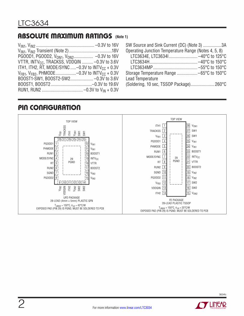
PIN FUNCTIONSPGOOD1 (Pin 1/Pin 4): Channel 1 Open-Drain Power Good Output Pin. PGOOD1 is pulled to ground when the voltage on the VFB1 pin is not within ±8% (typical) of the internal 0.6V reference. This threshold has 15mV of hysteresis.
PHMODE (Pin 2/Pin 5): Phase Select Input. Tie this pin to ground to force both channels to switch 90° out-of-phase. Tie this pin to INTVCC to force both channels to switch 180° out-of-phase. Do not float this pin.
RUN1 (Pin 3/Pin 6): Channel 1 Regulator Enable Pin. Enables channel 1 operation by tying RUN1 above 1.22V. Tying it below 1V places Channel 1 into shutdown. Do not float this pin.
MODE/SYNC (Pin 4/Pin 7): Channel 1 Mode Select and External Synchronization Input. Tie this pin to ground to force continuous synchronous operation on Channel 1. Floating this pin or tying it to INTVCC enables high efficiency Burst Mode® operation at light loads. Channel 2 operation is forced continuous regardless of the state of this pin. Drive this pin with a clock to synchronize the LTC3634 switching frequency. An internal phase-locked loop will force the bottom power NMOS’s turn-on signal to be synchronized with the rising edge of the CLKIN signal. When this pin is driven with a clock, forced continuous mode is automatically selected.
RT (Pin 5/Pin 8): Oscillator Frequency Program Pin. Connect an external resistor (between 80k to 640k) from this pin to SGND in order to program the frequency from 500kHz to 4MHz. When RT is tied to INTVCC, the switch-ing frequency will default to 2MHz. See the Applications Information section.
RUN2 (Pin 6/Pin 9): Channel 2 Regulator Enable Pin. Enables channel 2 operation by tying RUN2 above 1.22V. Tying it below 1V places Channel 2 into shutdown. Do not float this pin.
SGND (Pin 7/Pin 10): Signal Ground Pin. This pin should have a low noise connection to reference ground. The feedback resistor network, external compensation network, and RT resistor should be connected to this ground.
PGOOD2 (Pin 8/Pin 11): Channel 2 Open-Drain Power Good Output Pin. PGOOD2 is pulled to ground when the voltage on the VFB2 pin is not within 8% (typical) of VDDQIN • 0.5. This threshold has 15mV of hysteresis.
VFB2 (Pin 9/Pin 12): Channel 2 Output Feedback Voltage Pin. Input to the error amplifier that compares the feedback voltage to VTTR. Connect this pin directly to the output in order to set VOUT2 equal to VTTR.
VDDQIN (Pin 10/Pin 13): External Reference Input for Channel 2. An internal resistor divider sets the VTTR pin voltage to be equal to half the voltage applied to this input. Channel 2 uses the VTTR pin voltage as its error amplifier reference.
ITH2 (Pin 11/Pin 14): Channel 2 Error Amplifier Output and Switching Regulator Compensation Pin. Connect this pin to appropriate external components to compensate the regulator loop frequency response. See the Applications Information section for guidelines on component selection.
VON2 (Pin 12/Pin 15): On-Time Voltage Input for Chan-nel 2. This pin sets the voltage trip point for the on-time comparator. Tying this pin to the output voltage makes the on-time proportional to VOUT2 when VOUT2 < 3V. When VOUT2 > 3V, switching frequency may become higher than the set frequency (see the Applications Information sec-tion). The pin impedance is nominally 150kΩ.
SW2 (Pins 13, 14/Pins 16, 17): Channel 2 Switch Node Connection to External Inductor. Voltage swing of SW is from a diode voltage below ground to a diode voltage above VIN2.
VIN2 (Pins 15, 16/Pins 18, 19): Power Supply Input for Channel 2. Input voltage to the on-chip power MOSFETs on channel 2. This input is capable of operating from a supply voltage separate from VIN1.
BOOST2 (Pin 17/Pin 20): Boosted Floating Driver Supply for Channel 2. The (+) terminal of the bootstrap capacitor connects to this pin while the (–) terminal connects to the SW pin. The normal operation voltage swing of this pin ranges from a diode voltage drop below INTVCC up to VIN2 + INTVCC.
VTTR (Pin 18/Pin 21): Reference Output. This output is used to supply the VREF voltage for DDR memory. An on-chip buffer amplifier outputs a low noise reference voltage equal to VDDQIN/2. This output is capable of supplying 10mA. The buffer output can drive capacitive loads up to 0.01µF. A small series resistance (1Ω) between the output and the load further increases the amount of capacitance that the amplifier can drive. The error amplifier for channel 2 uses this voltage as its reference voltage.
INTVCC (Pin 19/Pin 22): Internal 3.3V Regulator Output. The internal gate drivers and control circuits are powered from this voltage. Decouple this pin to power ground with a minimum of 1μF low ESR ceramic capacitor. The internal regulator is disabled when both Channel 1 and Channel 2 are disabled with the RUN1/RUN2 inputs.
BOOST1 (Pin 20/Pin 23): Boosted Floating Driver Supply for Channel 1. The (+) terminal of the bootstrap capacitor connects to this pin while the (–) terminal connects to the SW pin. The normal operation voltage swing of this pin ranges from a diode voltage drop below INTVCC up to VIN1 + INTVCC.
VIN1 (Pins 21, 22/Pins 24, 25): Power Supply Input for Channel 1. Input voltage to the on-chip power MOSFETs on channel 1. The internal LDO for INTVCC is powered from this pin.
SW1 (Pins 23, 24/Pins 26, 27): Channel 1 Switch Node Connection to External Inductor. Voltage swing of SW is from a diode voltage drop below ground to a diode volt-age above VIN1.
VON1 (Pin 25/Pin 28): On-Time Voltage Input for Chan-nel 1. This pin sets the voltage trip point for the on-time comparator. Tying this pin to the regulated output voltage makes the on-time proportional to VOUT1 when VOUT1 < 3V. When VOUT1 > 3V, switching frequency may become
higher than the set frequency (see the Applications Infor-mation section). The pin impedance is nominally 150kΩ.
ITH1 (Pin 26/Pin 1): Channel 1 Error Amplifier Output and Switching Regulator Compensation Pin. Connect this pin to appropriate external components to compensate the regulator loop frequency response. See the Applications Information section for guidelines on component selection.
TRACKSS (Pin 27/Pin 2): Output Tracking and Soft-Start Input Pin for Channel 1. Forcing a voltage below 0.6V on this pin bypasses the internal reference input to the error amplifier. The LTC3634 will servo the FB pin to the TRACK voltage. Above 0.6V, the tracking function stops and the internal reference resumes control of the error amplifier. An internal 1.4μA pull-up current from INTVCC allows a soft-start function to be implemented by connecting a capacitor between this pin and SGND.
VFB1 (Pin 28/Pin 3): Channel 1 Output Feedback Voltage Pin. Input to the error amplifier that compares the feedback voltage to the internal 0.6V reference voltage. Connect this pin to a resistor divider network to program the desired output voltage. Connecting this pin to INTVCC configures the LTC3634 for 2-phase, single output operation; see the Applications Information section for full discussion.
PGND (Exposed Pad Pin 29/Exposed Pad Pin 29): Power Ground Pin. The (–) terminal of the input bypass capacitor, CIN, and the (–) terminal of the output capacitor, COUT, should be tied to this pin with a low impedance connec-tion. This pin must be soldered to the PCB to provide a low impedance electrical contact to power ground and good thermal contact to the PCB.
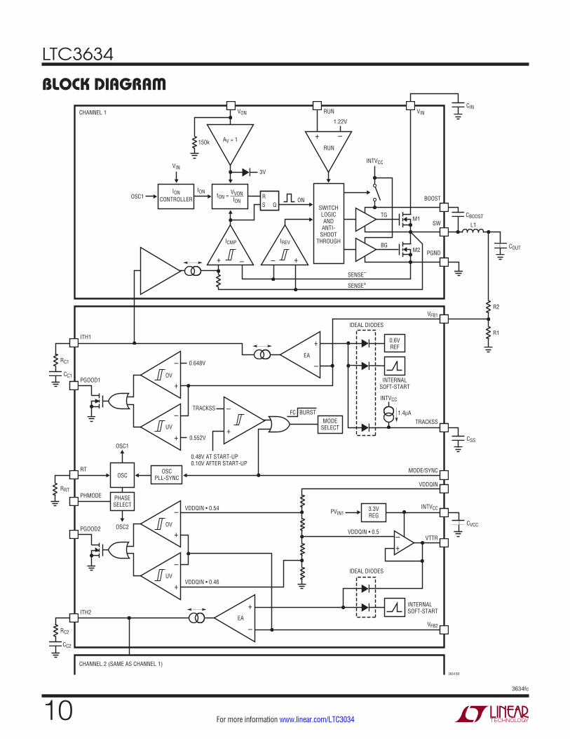
OPERATIONThe LTC3634 is a dual-channel, current mode monolithic step-down regulator designed to provide high efficiency power conversion for DDR memory supplies and bus ter-mination. Its unique controlled on-time architecture allows extremely low step-down ratios while maintaining a fast, constant switching frequency. Each channel is enabled by raising the voltage on the RUN pin above 1.22V nominally.
Main Control Loop
In normal operation, the internal top power MOSFET is turned on for a fixed interval determined by a one-shot timer (ON signal in the Block Diagram). When the top power MOSFET turns off, the bottom power MOSFET turns on until the current comparator ICMP trips, thus restarting the one-shot timer and initiating the next cycle. Inductor current is measured by sensing the voltage drop across the bottom power MOSFET. The voltage on the ITH pin sets the comparator threshold corresponding to inductor valley current. The error amplifier EA adjusts this ITH voltage by comparing the feedback signal VFB (derived from the output voltage) to an internal 0.6V reference voltage (chan-nel 1) or the VTTR voltage (channel 2). If the load current increases, it causes a drop in the feedback voltage relative to the reference voltage. The ITH voltage then rises until the average inductor current matches that of the load current.
The switching frequency is determined by the value of the RT resistor, which programs the current for the internal oscillator. An internal phase-locked loop servos the one-shot timer (ON signal) such that the internal oscillator edge phase-locks to the SW node edge, thus forcing a constant switching frequency. This unique controlled on-time architecture also allows the switching frequency to be synchronized to an external clock source when it is applied to the MODE/SYNC pin. Channel 1 defaults to forced continuous operation once the clock signal is ap-plied (channel 2 is always in forced continuous operation).
VTTR Output Buffer
The VTTR pin outputs a voltage equal to one half of VDDQIN. It is capable of sourcing/sinking 10mA and driving capacitive loads up to 0.01µF. A small series resistance (1Ω) between the output and the load further increases the amount of capacitance that the amplifier can
drive. The error amplifier for channel 2 uses this voltage as its reference voltage.
High Efficiency Burst Mode Operation
At light load currents, the inductor current can drop to zero and become negative. In Burst Mode operation (available only on channel 1), a current reversal comparator (IREV) detects the negative inductor current and shuts off the bot-tom power MOSFET, resulting in discontinuous operation and increased efficiency. Both power MOSFETs will remain off until the ITH voltage rises above the zero current level to initiate another cycle. During this time, the output capacitor supplies the load current and the part is placed into a low current sleep mode. Burst Mode operation is disabled by ty-ing the MODE/SYNC pin to ground, which forces continuous synchronous operation regardless of output load current.
Power Good Status Output
The PGOOD open-drain output will be pulled low if the regulator output exits a ±8% window around the regulation point. This threshold has 15mV of hysteresis relative to the VFB pin. To prevent unwanted PGOOD glitches during transients or dynamic VOUT changes, the LTC3634 PGOOD falling edge includes a filter time of approximately 40μs. For the VTT output (channel 2), VTTR is the regulation point. The PGOOD2 pin will always be low when the VTTR output voltage is less than 300mV.
VIN Overvoltage Protection
In order to protect the internal power MOSFET devices against long transient voltage events, the LTC3634 con-stantly monitors each VIN pin for an overvoltage condi-tion. When VIN rises above 17.5V, the regulator suspends operation by shutting off both power MOSFETs on the corresponding channel. Once VIN drops below 16.5V, the regulator immediately resumes normal operation. The regulator does not execute its soft-start function when exiting an overvoltage condition.
Out-Of-Phase Operation
Tying the PHMODE pin high sets the SW2 falling edge to be 180° out-of-phase with the SW1 falling edge. There is
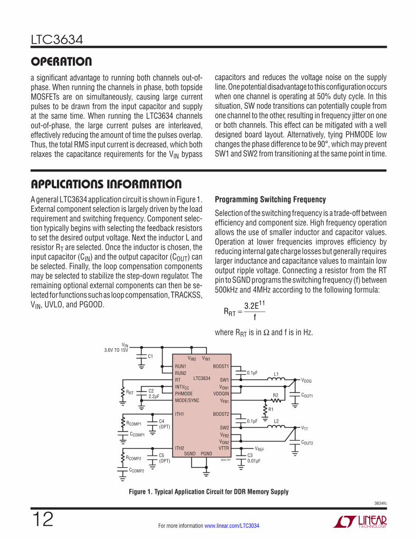
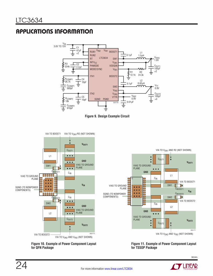
APPLICATIONS INFORMATIONA general LTC3634 application circuit is shown in Figure 1. External component selection is largely driven by the load requirement and switching frequency. Component selec-tion typically begins with selecting the feedback resistors to set the desired output voltage. Next the inductor L and resistor RT are selected. Once the inductor is chosen, the input capacitor (CIN) and the output capacitor (COUT) can be selected. Finally, the loop compensation components may be selected to stabilize the step-down regulator. The remaining optional external components can then be se-lected for functions such as loop compensation, TRACKSS, VIN, UVLO, and PGOOD.
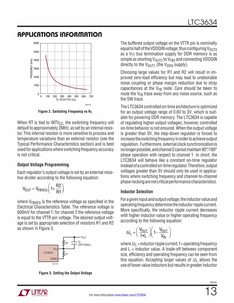
Programming Switching Frequency
Selection of the switching frequency is a trade-off between efficiency and component size. High frequency operation allows the use of smaller inductor and capacitor values. Operation at lower frequencies improves efficiency by reducing internal gate charge losses but generally requires larger inductance and capacitance values to maintain low output ripple voltage. Connecting a resistor from the RT pin to SGND programs the switching frequency (f) between 500kHz and 4MHz according to the following formula:
RRT =
3.2E11
f
where RRT is in Ω and f is in Hz.
RUN1RUN2RTINTVCCPHMODEMODE/SYNC
ITH1
ITH2
LTC3634
3634 F01
L1
R2
R1
0.1µF
C30.01µF
0.1µF
PGNDSGND
BOOST1
SW1VON1
VDDQINVFB1
BOOST2
SW2VFB2VON2VTTR
VIN1
VIN3.6V TO 15V
VIN2
L2
RCOMP2
RRT COUT1
VDDQ
COUT2
VTT
C5(OPT)
CCOMP2
RCOMP1
CCOMP1
C22.2µF
C1
C4(OPT)
VREF
Figure 1. Typical Application Circuit for DDR Memory Supply
a significant advantage to running both channels out-of-phase. When running the channels in phase, both topside MOSFETs are on simultaneously, causing large current pulses to be drawn from the input capacitor and supply at the same time. When running the LTC3634 channels out-of-phase, the large current pulses are interleaved, effectively reducing the amount of time the pulses overlap. Thus, the total RMS input current is decreased, which both relaxes the capacitance requirements for the VIN bypass
capacitors and reduces the voltage noise on the supply line. One potential disadvantage to this configuration occurs when one channel is operating at 50% duty cycle. In this situation, SW node transitions can potentially couple from one channel to the other, resulting in frequency jitter on one or both channels. This effect can be mitigated with a well designed board layout. Alternatively, tying PHMODE low changes the phase difference to be 90°, which may prevent SW1 and SW2 from transitioning at the same point in time.
When RT is tied to INTVCC, the switching frequency will default to approximately 2MHz, as set by an internal resis-tor. This internal resistor is more sensitive to process and temperature variations than an external resistor (see the Typical Performance Characteristics section) and is best used for applications where switching frequency accuracy is not critical.
Output Voltage Programming
Each regulator’s output voltage is set by an external resis-tive divider according to the following equation:
VOUT = VFBREG 1+
R2R1
where VFBREG is the reference voltage as specified in the Electrical Characteristics Table. The reference voltage is 600mV for channel 1; for channel 2 the reference voltage is equal to the VTTR pin voltage. The desired output volt-age is set by appropriate selection of resistors R1 and R2 as shown in Figure 3.
The buffered output voltage on the VTTR pin is nominally equal to half of the VDDQIN voltage; thus configuring VOUT2 as a VTT bus termination supply for DDR memory is as simple as shorting VOUT2 to VFB2 and connecting VDDQIN directly to the VOUT1 (the VDDQ supply).
Choosing large values for R1 and R2 will result in im-proved zero-load efficiency but may lead to undesirable noise coupling or phase margin reduction due to stray capacitances at the VFB node. Care should be taken to route the VFB trace away from any noise source, such as the SW trace.
The LTC3634 controlled on-time architecture is optimized for an output voltage range of 0.6V to 3V, which is suit-able for powering DDR memory. The LTC3634 is capable of regulating higher output voltages; however, controlled on-time behavior is not ensured. When the output voltage is greater than 3V, the step-down regulator is forced to increase the switching frequency in order to achieve output regulation. Furthermore, external clock synchronization is no longer possible, and channel 2 cannot maintain 90°/180° phase operation with respect to channel 1. In short, the LTC3634 will behave like a constant on-time regulator instead of a controlled on-time regulator. Therefore, output voltages greater than 3V should only be used in applica-tions where switching frequency and channel-to-channel phase-locking are not critical performance characteristics.
Inductor Selection
For a given input and output voltage, the inductor value and operating frequency determine the inductor ripple current. More specifically, the inductor ripple current decreases with higher inductor value or higher operating frequency according to the following equation:
∆IL =
VOUTf •L
1−VOUTVIN
where ΔIL = inductor ripple current, f = operating frequency and L = inductor value. A trade-off between component size, efficiency and operating frequency can be seen from this equation. Accepting larger values of ΔIL allows the use of lower value inductors but results in greater inductor
APPLICATIONS INFORMATIONcore loss, greater ESR loss in the output capacitor, and larger output voltage ripple. Generally, highest efficiency operation is obtained at low operating frequency with small ripple current.
A reasonable starting point is to choose a ripple current somewhere between 600mA and 1.2A peak-to-peak. Note that the largest ripple current occurs at the highest VIN. Exceeding 1.8A is not recommended in order to minimize output voltage ripple. To guarantee that ripple current does not exceed a specified maximum, the inductance should be chosen according to:
L =
VOUTf • ∆IL(MAX)
1−
VOUTVIN(MAX)
Once the value for L is known, the type of inductor must be selected. Actual core loss is independent of core size for a fixed inductor value, but is very dependent on the inductance selected. As the inductance increases, core losses decrease. Unfortunately, increased inductance requires more turns of wire, leading to increased DCR and copper loss.
Ferrite designs exhibit very low core loss and are pre-ferred at high switching frequencies, so design goals can concentrate on copper loss and preventing satura-tion. Ferrite core material saturates “hard”, which means that inductance collapses abruptly when the peak design current is exceeded. This results in an abrupt increase in inductor ripple current, so it is important to ensure that the core will not saturate.
Different core materials and shapes will change the size/current and price/current relationship of an inductor. Toroid or shielded pot cores in ferrite or permalloy materials are small and don’t radiate much energy, but generally cost more than powdered iron core inductors with similar characteristics. The choice of which style inductor to use mainly depends on the price versus size requirements and any radiated field/EMI requirements. Table 1 gives a sampling of available surface mount inductors.
The input capacitance, CIN, is needed to filter the trapezoi-dal wave current at the drain of the top power MOSFET. To prevent large voltage transients from occurring, a low ESR input capacitor sized for the maximum RMS current is recommended. The maximum RMS current for a single regulator is given by:
IRMS = IOUT(MAX)
VOUT VIN − VOUT( )VIN
When both regulators are active, the input current wave-form is significantly different. Furthermore, the input RMS current varies depending on each output’s load current as well as whether VTT is sinking or sourcing current.
When SW1 and SW2 operate 180° out-of-phase, the worst-case input RMS current occurs when the VTT supply is sinking current and VDDQ is sourcing the same amount of current. Knowing that VOUT2 = one-half VOUT1 in the DDR application, the input RMS current in this case is given by:
IRMS = IOUT(MAX) D1 1.5−D14
for D1 < 0.5
IRMS = IOUT(MAX) 1−34
D1 for D1 > 0.5
where D1 is the duty cycle of channel 1 (VDDQ supply). These equations show that maximum IRMS occurs at 50% duty cycle (VIN = 2 • VOUT1). This simple worst-case condition may be used for design as deviations in duty cycle do not offer significant relief. Note that ripple current ratings from capacitor manufacturers are often based on only 2000 hours of life which makes it advisable to further derate the capacitor, or choose a capacitor rated at a higher temperature than required.
Several capacitors may also be paralleled to meet size or height requirements in the design. For low input voltage applications, sufficient bulk input capacitance is needed to minimize transient effects during output load changes. Even though the LTC3634 design includes an overvoltage protection circuit, care must always be taken to ensure input voltage transients do not pose an overvoltage haz-ard to the part.
The selection of COUT is determined by the effective series resistance (ESR) that is required to minimize voltage ripple and load step transients as well as the amount of bulk capacitance that is necessary to ensure that the control loop is stable. Loop stability can be checked by viewing the load transient response. The output ripple, ΔVOUT, is approximated by:
∆VOUT < ∆IL ESR+
18 • f •COUT
When using low-ESR ceramic capacitors, it is more use-ful to choose the output capacitor value to fulfill a charge storage requirement. During a load step, the output capacitor
APPLICATIONS INFORMATIONmust instantaneously supply the current to support the load until the feedback loop raises the switch current enough to support the load. The time required for the feedback loop to respond is dependent on the compensation and the output capacitor size. Typically, three to four cycles are required to respond to a load step, but only in the first cycle does the output drop linearly. The output droop, VDROOP, is usually about three times the linear drop of the first cycle, provided the loop crossover frequency is maximized. Thus, a good place to start is with the output capacitor size of approximately:
COUT ≈
3• ∆IOUTf • VDROOP
Though this equation provides a good approximation, more capacitance may be required depending on the duty cycle and load step requirements. The actual VDROOP should be verified by applying a load step to the output.
Using Ceramic Input and Output Capacitors
Higher values, lower cost ceramic capacitors are available in small case sizes. Their high ripple current, high voltage rating and low ESR make them ideal for switching regulator applications. However, due to the self-resonant and high-Q characteristics of some types of ceramic capacitors, care must be taken when these capacitors are used at the input. When a ceramic capacitor is used at the input and the power is supplied by a wall adapter through long wires, a load step at the output can induce ringing at the VIN input. At best, this ringing can couple to the output and be mistaken as loop instability. At worst, a sudden inrush of current through the long wires can potentially cause a voltage spike at VIN large enough to damage the part. For a more detailed discussion, refer to Application Note 88.
When choosing the input and output ceramic capacitors, choose the X5R and X7R dielectric formulations. These dielectrics have the best temperature and voltage char-acteristics of all the ceramics for a given value and size.
Loop compensation is a complicated subject and Applica-tion Note 76 is recommended reading for a full discussion on maximizing loop bandwidth in a current mode switch-ing regulator. This section will provide a quick method on choosing proper components to compensate the LTC3634 regulators.
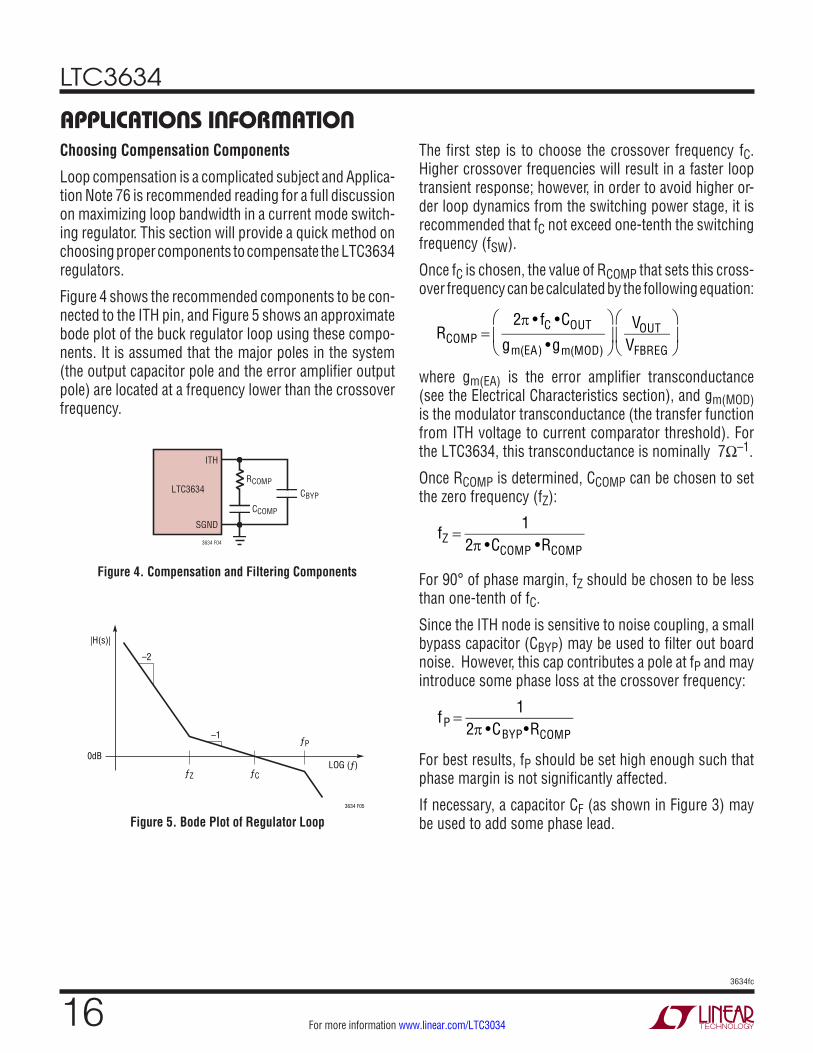
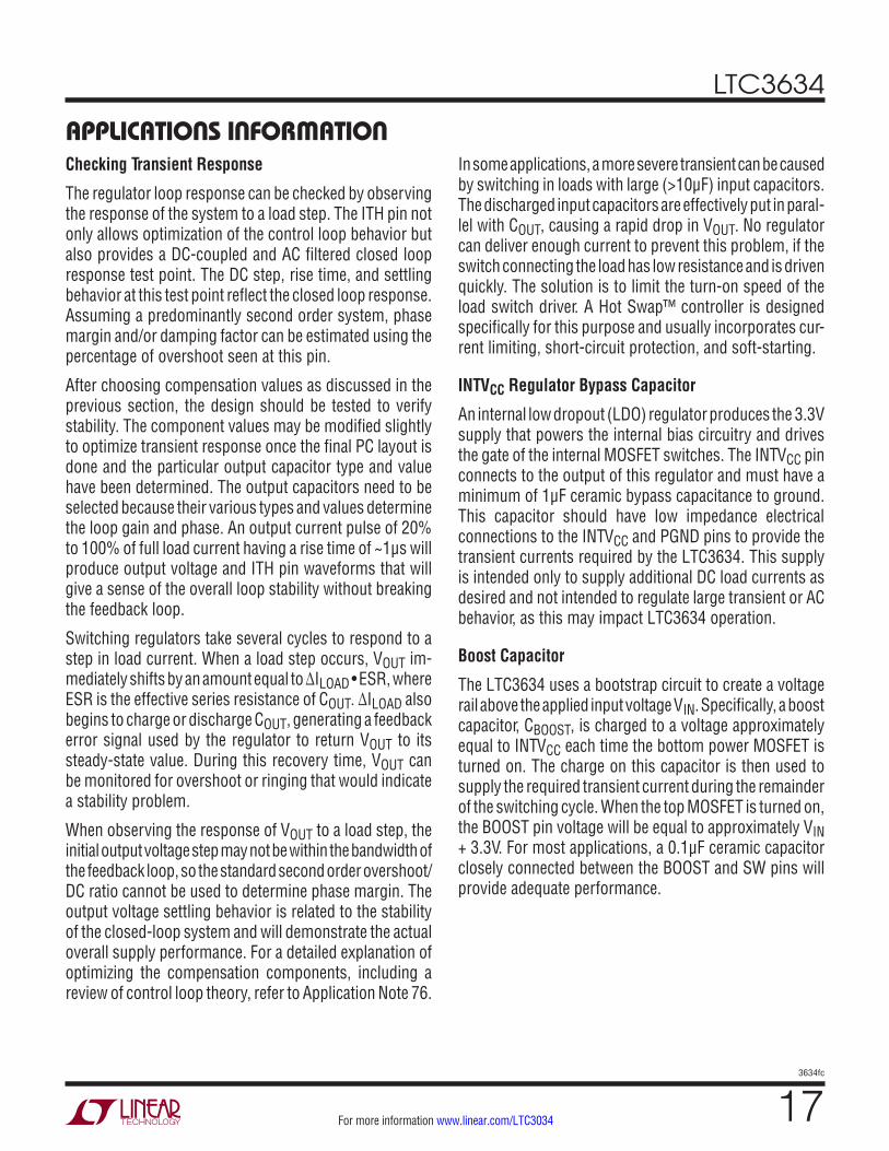
Figure 4 shows the recommended components to be con-nected to the ITH pin, and Figure 5 shows an approximate bode plot of the buck regulator loop using these compo-nents. It is assumed that the major poles in the system (the output capacitor pole and the error amplifier output pole) are located at a frequency lower than the crossover frequency.
Figure 4. Compensation and Filtering Components
Figure 5. Bode Plot of Regulator Loop
ƒP
LOG (ƒ)ƒCƒZ
3634 F05
–1
0dB
|H(s)|
–2
The first step is to choose the crossover frequency fC. Higher crossover frequencies will result in a faster loop transient response; however, in order to avoid higher or-der loop dynamics from the switching power stage, it is recommended that fC not exceed one-tenth the switching frequency (fSW).
Once fC is chosen, the value of RCOMP that sets this cross-over frequency can be calculated by the following equation:
RCOMP =
2π • fC •COUT
gm(EA) •gm(MOD)
VOUTVFBREG
where gm(EA) is the error amplifier transconductance (see the Electrical Characteristics section), and gm(MOD) is the modulator transconductance (the transfer function from ITH voltage to current comparator threshold). For the LTC3634, this transconductance is nominally 7Ω–1.
Once RCOMP is determined, CCOMP can be chosen to set the zero frequency (fZ):
fZ =
12π •CCOMP •RCOMP
For 90° of phase margin, fZ should be chosen to be less than one-tenth of fC.
Since the ITH node is sensitive to noise coupling, a small bypass capacitor (CBYP) may be used to filter out board noise. However, this cap contributes a pole at fP and may introduce some phase loss at the crossover frequency:
fP =
12π •CBYP•RCOMP
For best results, fP should be set high enough such that phase margin is not significantly affected.
If necessary, a capacitor CF (as shown in Figure 3) may be used to add some phase lead.
The regulator loop response can be checked by observing the response of the system to a load step. The ITH pin not only allows optimization of the control loop behavior but also provides a DC-coupled and AC filtered closed loop response test point. The DC step, rise time, and settling behavior at this test point reflect the closed loop response. Assuming a predominantly second order system, phase margin and/or damping factor can be estimated using the percentage of overshoot seen at this pin.
After choosing compensation values as discussed in the previous section, the design should be tested to verify stability. The component values may be modified slightly to optimize transient response once the final PC layout is done and the particular output capacitor type and value have been determined. The output capacitors need to be selected because their various types and values determine the loop gain and phase. An output current pulse of 20% to 100% of full load current having a rise time of ~1μs will produce output voltage and ITH pin waveforms that will give a sense of the overall loop stability without breaking the feedback loop.
Switching regulators take several cycles to respond to a step in load current. When a load step occurs, VOUT im-mediately shifts by an amount equal to ΔILOAD • ESR, where ESR is the effective series resistance of COUT. ΔILOAD also begins to charge or discharge COUT, generating a feedback error signal used by the regulator to return VOUT to its steady-state value. During this recovery time, VOUT can be monitored for overshoot or ringing that would indicate a stability problem.
When observing the response of VOUT to a load step, the initial output voltage step may not be within the bandwidth of the feedback loop, so the standard second order overshoot/ DC ratio cannot be used to determine phase margin. The output voltage settling behavior is related to the stability of the closed-loop system and will demonstrate the actual overall supply performance. For a detailed explanation of optimizing the compensation components, including a review of control loop theory, refer to Application Note 76.
APPLICATIONS INFORMATIONIn some applications, a more severe transient can be caused by switching in loads with large (>10μF) input capacitors. The discharged input capacitors are effectively put in paral-lel with COUT, causing a rapid drop in VOUT. No regulator can deliver enough current to prevent this problem, if the switch connecting the load has low resistance and is driven quickly. The solution is to limit the turn-on speed of the load switch driver. A Hot Swap™ controller is designed specifically for this purpose and usually incorporates cur-rent limiting, short-circuit protection, and soft-starting.
INTVCC Regulator Bypass Capacitor
An internal low dropout (LDO) regulator produces the 3.3V supply that powers the internal bias circuitry and drives the gate of the internal MOSFET switches. The INTVCC pin connects to the output of this regulator and must have a minimum of 1μF ceramic bypass capacitance to ground. This capacitor should have low impedance electrical connections to the INTVCC and PGND pins to provide the transient currents required by the LTC3634. This supply is intended only to supply additional DC load currents as desired and not intended to regulate large transient or AC behavior, as this may impact LTC3634 operation.
Boost Capacitor
The LTC3634 uses a bootstrap circuit to create a voltage rail above the applied input voltage VIN. Specifically, a boost capacitor, CBOOST, is charged to a voltage approximately equal to INTVCC each time the bottom power MOSFET is turned on. The charge on this capacitor is then used to supply the required transient current during the remainder of the switching cycle. When the top MOSFET is turned on, the BOOST pin voltage will be equal to approximately VIN + 3.3V. For most applications, a 0.1μF ceramic capacitor closely connected between the BOOST and SW pins will provide adequate performance.
The minimum off-time is the smallest amount of time that the LTC3634 can turn on the bottom power MOSFET, trip the current comparator and turn the power MOSFET back off. This time is typically 40ns. For the controlled on-time control architecture, the minimum off-time limit imposes a maximum duty cycle of:
DCMAX = 1– f • (tOFF(MIN) + 2 • tDEAD)
where f is the switching frequency, tDEAD is the nonoverlap time of the switches, or dead time (typically 15ns), and tOFF(MIN) is the minimum off-time. If the maximum duty cycle is surpassed, due to a decreasing input voltage for example, the output will drop out of regulation. The minimum input voltage to avoid this dropout condition is:
VIN(MIN) =VOUT
1− f • tOFF(MIN) +2• tDEAD( )Conversely, the minimum on-time is the smallest dura-tion of time in which the top power MOSFET can be in its ON state. This time is typically 20ns. In continuous mode operation, the minimum on-time limit imposes a minimum duty cycle of:
DCMIN = (f • tON(MIN))
where tON(MIN) is the minimum on-time. As the equation shows, reducing the operating frequency will alleviate the minimum duty cycle constraint.
When the regulator output is sinking current, the effective minimum on-time of the converter will be increased by the non-overlap time of the power MOSFETs (or the “dead-time”) during each SW node transition. This “dead-time” is nominally 15ns, so when sinking current, the minimum on-time is effectively 15ns + 15ns + 20ns = 50ns.
If the minimum on-time constraint is violated, the converter will automatically reduce its own switching frequency in order to maintain output regulation. Once the converter reduces its switching frequency, the phase information is lost and the two channels will switch asynchronously.
Furthermore, the regulator may need to be compensated more conservatively due to the lower switching frequency.
MODE/SYNC Operation
The MODE/SYNC pin is a multipurpose pin allowing both mode selection and operating frequency synchronization. Floating this pin or connecting it to INTVCC enables Burst Mode operation on channel 1 for superior efficiency at light load currents at the expense of slightly higher out-put voltage ripple. When the MODE/SYNC pin is tied to ground, forced continuous mode operation is selected, creating the lowest fixed output ripple at the expense of light load efficiency.
The LTC3634 will detect the presence of the external clock signal on the MODE/SYNC pin and synchronize the internal oscillator to the phase and frequency of the in-coming clock. The presence of an external clock will place both regulators into forced continuous mode operation. Although the RT resistor is not strictly necessary when synchronizing to an external clock, it is recommended to use a RT resistor that matches the nominal external clock frequency in order to keep the switching regulator biased correctly whenever the external clock signal is suddenly removed or reapplied.
Channel 1 Output Voltage Tracking and Soft-Start
The LTC3634 allows the user to control the output voltage ramp rate of channel 1 by means of the TRACKSS pin. From 0 to 0.6V, the TRACKSS voltage will override the internal 0.6V reference input to the error amplifier, thus regulating the feedback voltage to that of the TRACKSS pin. When TRACKSS is above 0.6V, tracking is disabled and the feedback voltage will regulate to the internal reference voltage.
The voltage at the TRACKSS pin may be driven from an external source, or alternatively, the user may leverage the internal 1.4μA pull-up current source to implement a soft-start function by connecting an external capacitor (CSS) from the TRACKSS pin to ground. The relationship between output rise time and TRACKSS capacitance is given by:
A default internal soft-start ramp forces a minimum soft-start time of 400μs by overriding the TRACKSS pin input during this time period. Hence, capacitance values less than approximately 1000pF will not significantly affect soft-start behavior.
Start-Up Behavior
Upon start-up, both channels immediately default to discontinuous operation. Channel 1 will remain in dis-continuous Burst Mode operation until its output rises to greater than 80% of its final value (VFB > 480mV). Once the output exceeds this voltage, the operating mode of the regulator switches to the mode selected by the MODE/SYNC pin as described above. During normal operation, if the output drops below 10% of its final value (as it may when tracking down, for instance), the regulator will automatically switch to Burst Mode operation to prevent inductor saturation and improve TRACKSS pin accuracy.
Channel 2 (the VTT termination supply) remains in discon-tinuous operation until its output rises above 300mV, at which point it will automatically switch to forced continuous operation. This ensures that the regulator output has suf-
APPLICATIONS INFORMATIONficient voltage to discharge the inductor in continuous mode and prevent excessive build-up of energy in the inductor.
Output Power Good
The PGOOD output of the LTC3634 is driven by a 15Ω (typical) open-drain pull-down device. If the output volt-age exits an 8% (typical) regulation window around the target regulation point, the open-drain output will pull down with 15Ω output resistance to ground, thus dropping the PGOOD pin voltage. This pull-down device will not shut off until the output re-enters this window and overcomes a small amount of hysteresis. This behavior is described in Figure 6.
A filter time of 40μs (typical) acts to prevent unwanted PGOOD output changes during VOUT transient events. As a result, the output voltage must exit the 8% regulation window for 40μs before the PGOOD pin pulls to ground. Conversely, the output voltage must be within the target regulation window for 40μs before the PGOOD pin pulls high.
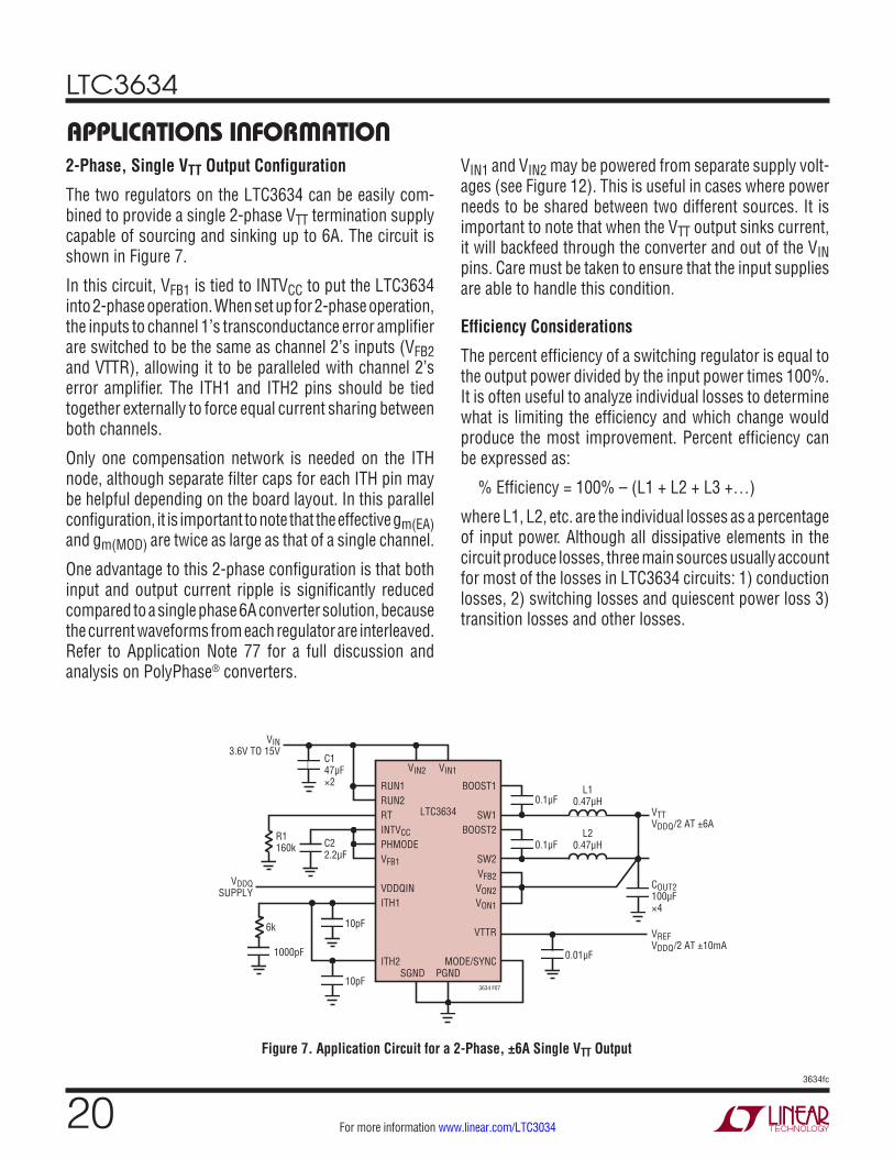
APPLICATIONS INFORMATION2-Phase, Single VTT Output Configuration
The two regulators on the LTC3634 can be easily com-bined to provide a single 2-phase VTT termination supply capable of sourcing and sinking up to 6A. The circuit is shown in Figure 7.
In this circuit, VFB1 is tied to INTVCC to put the LTC3634 into 2-phase operation. When set up for 2-phase operation, the inputs to channel 1’s transconductance error amplifier are switched to be the same as channel 2’s inputs (VFB2 and VTTR), allowing it to be paralleled with channel 2’s error amplifier. The ITH1 and ITH2 pins should be tied together externally to force equal current sharing between both channels.
Only one compensation network is needed on the ITH node, although separate filter caps for each ITH pin may be helpful depending on the board layout. In this parallel configuration, it is important to note that the effective gm(EA) and gm(MOD) are twice as large as that of a single channel.
One advantage to this 2-phase configuration is that both input and output current ripple is significantly reduced compared to a single phase 6A converter solution, because the current waveforms from each regulator are interleaved. Refer to Application Note 77 for a full discussion and analysis on PolyPhase® converters.
VIN1 and VIN2 may be powered from separate supply volt-ages (see Figure 12). This is useful in cases where power needs to be shared between two different sources. It is important to note that when the VTT output sinks current, it will backfeed through the converter and out of the VIN pins. Care must be taken to ensure that the input supplies are able to handle this condition.
Efficiency Considerations
The percent efficiency of a switching regulator is equal to the output power divided by the input power times 100%. It is often useful to analyze individual losses to determine what is limiting the efficiency and which change would produce the most improvement. Percent efficiency can be expressed as:
% Efficiency = 100% – (L1 + L2 + L3 +…)
where L1, L2, etc. are the individual losses as a percentage of input power. Although all dissipative elements in the circuit produce losses, three main sources usually account for most of the losses in LTC3634 circuits: 1) conduction losses, 2) switching losses and quiescent power loss 3) transition losses and other losses.
Figure 7. Application Circuit for a 2-Phase, ±6A Single VTT Output
1. Conduction losses are calculated from the DC resis-tances of the internal switches, RSW, and external inductor, RL. In continuous mode, the average output current flows through inductor L but is “chopped” between the internal top and bottom power MOSFETs. Thus, the series resistance looking into the SW pin is a function of both top and bottom MOSFET RDS(ON) and the duty cycle (DC) as follows:
RSW = (RDS(ON)TOP)(DC) + (RDS(ON)BOT)(1 – DC)
The RDS(ON) for both the top and bottom MOSFETs can be obtained from the Typical Performance Characteristics curves. So to calculate conduction losses:
Conduction Loss = IOUT2 (RSW + RL)
2. The internal LDO supplies the power to the INTVCC rail. The total power loss here is the sum of the switching losses and quiescent current losses from the control circuitry.
Each time a power MOSFET gate is switched from low to high to low again, a packet of charge dQ moves from VIN to ground. The resulting dQ/dt is a current out of INTVCC that is typically much larger than the DC control bias current. In continuous mode, IGATECHG = f • (QT + QB), where QT and QB are the gate charges of the internal top and bottom power MOSFETs and f is the switching frequency. For estimation purposes, (QT + QB) on each LTC3634 regulator channel is approximately 2.3nC.
To calculate the total power loss from the LDO load, simply add the gate charge current and quiescent cur-rent and multiply by VIN:
PLDO = (IGATECHG + IQ) • VIN
3. Other hidden losses such as transition loss, copper trace resistances, and internal load currents can account for additional efficiency degradations in the overall power system. Transition loss arises from the brief amount of time the top power MOSFET spends in the saturated region during switch node transitions. The LTC3634 internal power devices switch quickly enough that these losses are not significant compared to other sources. Other losses, including diode conduction losses during dead-time and inductor core losses, generally account for less than 2% total additional loss.
Thermal Considerations
The LTC3634 requires the exposed package back-plane metal (PGND) to be well soldered to the PC board to provide good thermal contact. This gives the QFN and TSSOP packages exceptional thermal properties, which are necessary to prevent excessive self-heating of the part in normal operation.
In a majority of applications, the LTC3634 does not dis-sipate much heat due to its high efficiency and low thermal resistance of its exposed-back QFN package. However, in applications where the LTC3634 is running at high ambi-ent temperature, high VIN, high switching frequency, and maximum output current load, the heat dissipated may exceed the maximum junction temperature of the part. If the junction temperature reaches approximately 170°C, both power switches will be turned off until the temperature returns to 160°C.
To prevent the LTC3634 from exceeding the maximum junction temperature of 125°C, the user will need to do some thermal analysis. The goal of the thermal analysis is to determine whether the power dissipated exceeds the maximum junction temperature of the part. The tempera-ture rise is given by:
TRISE = PD • θJA
As an example, consider the case when the LTC3634 is used to power DDR2 SDRAM and is used in an application where maximum ambient temperature is 70°C, VIN = 12V, frequency = 1MHz, VDDQ = 1.8V, VTT = 0.9V, and ILOAD = 2A for both channels.
From the RDS(ON) graphs in the Typical Performance Characteristics section, the top switch on-resistance is nominally 140mΩ and the bottom switch on-resistance is nominally 75mΩ at 70°C ambient. For the VDDQ supply, the equivalent power MOSFET resistance RSW1 is:
RDS(ON)TOP •
1.8V12V
+RDS(ON)BOT •10.2V12V
= 84.8mΩ
The same calculation to the VTT supply (0.9V), yields RSW2 = 79.9mΩ.
From the previous section’s discussion on gate drive, we estimate the total gate charge current for each regulator to
APPLICATIONS INFORMATIONbe 1MHz • 2.3nC = 2.3mA, and the total IQ of both chan-nels is 1.3mA (see the Electrical Characteristics section). Therefore, the total power dissipated by both regulators is:
The QFN 4mm × 5mm package junction-to-ambient thermal resistance, θJA, is around 43°C/W. Therefore, the junction temperature of the regulator operating in a 70°C ambient temperature is approximately:
TJ = 0.730W • 43°C/W + 70°C = 101°C
which is below the maximum junction temperature of 125°C. With higher ambient temperatures, a heat sink or cooling fan should be considered to drop the junction-to-ambient thermal resistance. Alternatively, the exposed pad TSSOP package may be a better choice for high power applications, since it has better thermal properties than the QFN package.
Remembering that the above junction temperature is ob-tained from a RDS(ON) at 70°C, we might recalculate the junction temperature based on a higher RDS(ON) since it increases with temperature. Redoing the calculation as-suming that RSW increased 12% at 101°C yields a new junction temperature of 105°C.
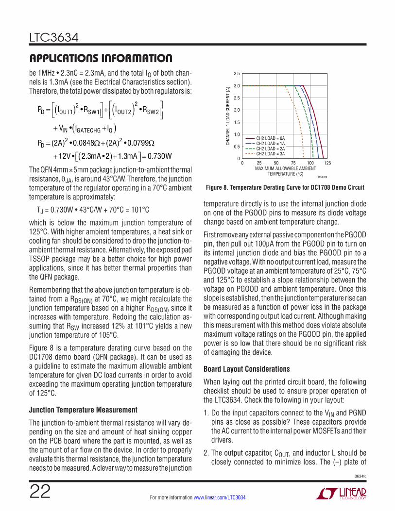
Figure 8 is a temperature derating curve based on the DC1708 demo board (QFN package). It can be used as a guideline to estimate the maximum allowable ambient temperature for given DC load currents in order to avoid exceeding the maximum operating junction temperature of 125°C.
Junction Temperature Measurement
The junction-to-ambient thermal resistance will vary de-pending on the size and amount of heat sinking copper on the PCB board where the part is mounted, as well as the amount of air flow on the device. In order to properly evaluate this thermal resistance, the junction temperature needs to be measured. A clever way to measure the junction
Figure 8. Temperature Derating Curve for DC1708 Demo Circuit
temperature directly is to use the internal junction diode on one of the PGOOD pins to measure its diode voltage change based on ambient temperature change.
First remove any external passive component on the PGOOD pin, then pull out 100μA from the PGOOD pin to turn on its internal junction diode and bias the PGOOD pin to a negative voltage. With no output current load, measure the PGOOD voltage at an ambient temperature of 25°C, 75°C and 125°C to establish a slope relationship between the voltage on PGOOD and ambient temperature. Once this slope is established, then the junction temperature rise can be measured as a function of power loss in the package with corresponding output load current. Although making this measurement with this method does violate absolute maximum voltage ratings on the PGOOD pin, the applied power is so low that there should be no significant risk of damaging the device.
Board Layout Considerations
When laying out the printed circuit board, the following checklist should be used to ensure proper operation of the LTC3634. Check the following in your layout:
1. Do the input capacitors connect to the VIN and PGND pins as close as possible? These capacitors provide the AC current to the internal power MOSFETs and their drivers.
2. The output capacitor, COUT, and inductor L should be closely connected to minimize loss. The (–) plate of
COUT should be closely connected to both PGND and the (–) plate of CIN.
3. The resistive divider, (e.g. R1 and R2 in Figure 1) must be connected between the (+) plate of COUT and a ground line terminated near SGND. The feedback signal VFB should be routed away from noisy components and traces, such as the SW line, and its trace length should be minimized. In addition, the RT resistor and loop compensation components should be terminated to SGND.
4. Keep sensitive components away from the SW pin. The RT resistor, the compensation components, the feedback resistors, and the INTVCC bypass capacitor should all be routed away from the SW trace and the inductor L.
5. A ground plane is preferred, but if not available, the signal and power grounds should be segregated with both connecting to a common, low noise reference point. The connection to the PGND pin should be made with a minimal resistance trace from the reference point.
6. Flood all unused areas on all layers with copper in order to reduce the temperature rise of power components. These copper areas should be connected to the exposed backside of the package (PGND). Refer to Figures 10 and 11 for board layout examples.
Design Example
As a design example, consider using the LTC3634 (as shown in Figure 1) to power DDR2 SDRAM with the fol-lowing specifications: VIN(MAX) = 13.2V, IOUT(MAX) = ±2A, f = 1MHz, VDROOP(VDDQ) < 60mV, VDROOP(VTT) < 30mV. The following discussion will use equations from the previous sections.
First, the correct RT resistor value for 1MHz switching frequency must be chosen. Based on previous discus-sions, RT is calculated to be
RT =
3.2E11
f
= 320kΩ
The closest standard value is 324k.
Next, select values for R1 and R2 to set channel 1 (VDDQ) to be 1.8V for DDR2 SDRAM. Choosing R1 to be 12.1k, R2 is calculated to be:
R2= 12.1k •
1.8V0.6V
−1
= 24.2k
The closest standard value is 24.3k. Tying VDDQIN to VOUT1 sets VOUT2 to be half of VOUT1.
Next, we can pick inductor values for both the VDDQ and VTT outputs. Choosing inductor current ripple to be 1A at maximum VIN:
L1=1.8V
1MHz •1A
1−
1.8V13.2V
= 1.55µH
L2=0.9V
1MHz •1A
1−
0.9V13.2V
= 0.838µH
Standard values of 1.5μH and 0.82µH should be used.
Ceramic caps will be used for COUT and will be selected based on the charge storage requirement. Assuming a worst case 4A load step (–2A to 2A):
COUT1 ≈3• 4A
1MHz •60mV= 200µF
COUT2 ≈3• 4A
1MHz •30mV= 400µF
Lastly, we will choose compensation components. Choos-ing the crossover frequency fC = 50kHz:
RCOMP1 =2π •50kHz •200µF
1mΩ−1 •7Ω−1
1.8V0.6V
= 27kΩ
RCOMP2 =2π •50kHz • 400µF
1mΩ−1 •7Ω−1
0.9V0.9V
= 18kΩ
Choosing the zero frequency to be 10kHz yields CCOMP1 = 589pF and CCOMP2 = 884pF. The closest standard values for the compensation components are 26.7k, 18k, 560pF and 910pF, respectively.
NOTE:1. DRAWING PROPOSED TO BE MADE A JEDEC PACKAGE OUTLINE MO-220 VARIATION (WXXX-X).2. DRAWING NOT TO SCALE3. ALL DIMENSIONS ARE IN MILLIMETERS4. DIMENSIONS OF EXPOSED PAD ON BOTTOM OF PACKAGE DO NOT INCLUDE MOLD FLASH. MOLD FLASH, IF PRESENT, SHALL NOT EXCEED 0.15mm ON ANY SIDE5. EXPOSED PAD SHALL BE SOLDER PLATED6. SHADED AREA IS ONLY A REFERENCE FOR PIN 1 LOCATION ON THE TOP AND BOTTOM OF PACKAGE
PIN 1TOP MARK(NOTE 6)
0.40 ±0.10
27 28
1
2
BOTTOM VIEW—EXPOSED PAD
3.50 REF
0.75 ±0.05 R = 0.115TYP
R = 0.05TYP
PIN 1 NOTCHR = 0.20 OR 0.35× 45° CHAMFER
0.25 ±0.05
0.50 BSC
0.200 REF
0.00 – 0.05
(UFD28) QFN 0506 REV B
RECOMMENDED SOLDER PAD PITCH AND DIMENSIONSAPPLY SOLDER MASK TO AREAS THAT ARE NOT SOLDERED
0.70 ±0.05
0.25 ±0.050.50 BSC
2.50 REF
3.50 REF4.10 ±0.055.50 ±0.05
2.65 ±0.05
3.10 ±0.054.50 ±0.05
PACKAGE OUTLINE
2.65 ±0.10
3.65 ±0.10
3.65 ±0.05
UFD Package28-Lead Plastic QFN (4mm × 5mm)
(Reference LTC DWG # 05-08-1712 Rev B)
Please refer to http://www.linear.com/product/LTC3634#packaging for the most recent package drawings.
Information furnished by Linear Technology Corporation is believed to be accurate and reliable. However, no responsibility is assumed for its use. Linear Technology Corporation makes no representa-tion that the interconnection of its circuits as described herein will not infringe on existing patent rights.
REVISION HISTORYREV DATE DESCRIPTION PAGE NUMBER
A 09/13 Clarified Absolute Maximum Ratings, added H and MP grades to Order Information.Clarified parametric data.Clarified graphs.Clarified RUN1, RUN2 pin function, INTVCC.Clarified minimum on-time description.Clarified maximum junction temperature in Thermal Considerations.Clarified Related Parts, added LTC3786 and LTC3633A.
23, 45, 67, 8182128
B 12/13 Clarified dead-time from 10ns to 15ns. 18
C 01/16 Added package option for mini reels Expanded VTTR pin description Expanded description in VTTR Output Buffer