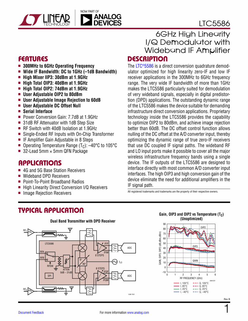
LTC5586 1 Rev B For more information www.analog.com Document Feedback TYPICAL APPLICATION FEATURES DESCRIPTION 6GHz High Linearity I/Q Demodulator with Wideband IF Amplifier Dual Band Transmitter with DPD Receiver Gain, OIP3 and OIP2 vs Temperature (T C ) (Unoptimized) n 4G and 5G Base Station Receivers n Wideband DPD Receivers n Point-To-Point Broadband Radios n High Linearity Direct Conversion I/Q Receivers n Image Rejection Receivers n 300MHz to 6GHz Operating Frequency n Wide IF Bandwidth: DC to 1GHz (–1dB Bandwidth) n High Mixer IIP3: 30dBm at 1.9GHz n High Total OIP3: 40dBm at 1.9GHz n High Total OIP2: 74dBm at 1.9GHz n User Adjustable OIP2 to 80dBm n User Adjustable Image Rejection to 60dB n User Adjustable DC Offset Null n Serial Interface n Power Conversion Gain: 7.7dB at 1.9GHz n 31dB RF Attenuator with 1dB Step Size n RF Switch with 40dB Isolation at 1.9GHz n Single-Ended RF Inputs with On-Chip Transformer n IF Amplifier Gain Adjustable in 8 Steps n Operating Temperature Range (T C ): –40°C to 105°C n 32-Lead 5mm × 5mm QFN Package The LTC ® 5586 is a direct conversion quadrature demod- ulator optimized for high linearity zero-IF and low IF receiver applications in the 300MHz to 6GHz frequency range. The very wide IF bandwidth of more than 1GHz makes the LTC5586 particularly suited for demodulation of very wideband signals, especially in digital predistor- tion (DPD) applications. The outstanding dynamic range of the LTC5586 makes the device suitable for demanding infrastructure direct conversion applications. Proprietary technology inside the LTC5586 provides the capability to optimize OIP2 to 80dBm, and achieve image rejection better than 60dB. The DC offset control function allows nulling of the DC offset at the A/D converter input, thereby optimizing the dynamic range of true zero-IF receivers that use DC coupled IF signal paths. The wideband RF and LO input ports make it possible to cover all the major wireless infrastructure frequency bands using a single device. The IF outputs of the LTC5586 are designed to interface directly with most common A/D converter input interfaces. The high OIP3 and high conversion gain of the device eliminate the need for additional amplifiers in the IF signal path. All registered trademarks and trademarks are the property of their respective owners. LTC5586 5586 TA01 ATTEN 0dB – 31dB 0º 90º ADC ADC RFB PA 1 PA 2 RFSW RF 1 RF 2 f LO SPI IFIP IFIM IFQP IFQM RFA 8 STEPS 8 STEPS 0 1 2 3 4 5 6 90 80 70 60 50 40 30 20 10 0 -10 RF FREQUENCY (GHz) GAIN, OIP3, OIP2 (dB,dBm,dBm) 5586 G01 GAIN OIP3 OIP2 I, 105°C I, 85°C I, 25°C I, –40°C Q, 105°C Q, 85°C Q, 25°C Q, –40°C APPLICATIONS
Transcript
LTC5586
1Rev B
For more information www.analog.comDocument Feedback
TYPICAL APPLICATION
FEATURES DESCRIPTION
6GHz High Linearity I/Q Demodulator with Wideband IF Amplifier
Dual Band Transmitter with DPD Receiver
Gain, OIP3 and OIP2 vs Temperature (TC) (Unoptimized)
n 4G and 5G Base Station Receivers n Wideband DPD Receivers n Point-To-Point Broadband Radios n High Linearity Direct Conversion I/Q Receivers n Image Rejection Receivers
n 300MHz to 6GHz Operating Frequency n Wide IF Bandwidth: DC to 1GHz (–1dB Bandwidth) n High Mixer IIP3: 30dBm at 1.9GHz n High Total OIP3: 40dBm at 1.9GHz n High Total OIP2: 74dBm at 1.9GHz n User Adjustable OIP2 to 80dBm n User Adjustable Image Rejection to 60dB n User Adjustable DC Offset Null n Serial Interface n Power Conversion Gain: 7.7dB at 1.9GHz n 31dB RF Attenuator with 1dB Step Size n RF Switch with 40dB Isolation at 1.9GHz n Single-Ended RF Inputs with On-Chip Transformer n IF Amplifier Gain Adjustable in 8 Steps n Operating Temperature Range (TC): –40°C to 105°C n 32-Lead 5mm × 5mm QFN Package
The LTC®5586 is a direct conversion quadrature demod-ulator optimized for high linearity zero-IF and low IF receiver applications in the 300MHz to 6GHz frequency range. The very wide IF bandwidth of more than 1GHz makes the LTC5586 particularly suited for demodulation of very wideband signals, especially in digital predistor-tion (DPD) applications. The outstanding dynamic range of the LTC5586 makes the device suitable for demanding infrastructure direct conversion applications. Proprietary technology inside the LTC5586 provides the capability to optimize OIP2 to 80dBm, and achieve image rejection better than 60dB. The DC offset control function allows nulling of the DC offset at the A/D converter input, thereby optimizing the dynamic range of true zero-IF receivers that use DC coupled IF signal paths. The wideband RF and LO input ports make it possible to cover all the major wireless infrastructure frequency bands using a single device. The IF outputs of the LTC5586 are designed to interface directly with most common A/D converter input interfaces. The high OIP3 and high conversion gain of the device eliminate the need for additional amplifiers in the IF signal path.All registered trademarks and trademarks are the property of their respective owners.
VCC, VCCN Supply Voltage (Note 21) ....... –0.3V to 5.5VOVDD, SDO Voltage (Note 18) ................... –0.3V to 3.8V RFA, RFB DC Voltage ...................................1.5V to 2.0VLOP, LOM DC Voltage .................................. 2.1V to 2.8VIFIM, IFIP, IFQP, IFQM DC Voltage ............. –0.3V to 3.5VAIM, AIP, AQM, AQP
DC Voltage ........................... VCC – 1.7V to VCC – 1.2VMIM, MIP, MQM, MQP
DC Voltage ........................... VCC – 1.7V to VCC – 1.2VVoltage on Any Other Pin .......................... –0.3V to 5.5VLOP, LOM, RFA, RFB Input Power (Note 17) ......+20dBmOutput Short Circuit Duration (Notes 14, 17) ... IndefiniteMaximum Junction Temperature (TJMAX) ............. 150°CCase Operating Temperature Range (TC) –40°C to 105°CStorage Temperature Range .................. –65°C to 150°C
(Note 1)
32 31 30 29 28 27
9 10 11
TOP VIEW
33GND
UH PACKAGE32-LEAD (5mm × 5mm) PLASTIC QFN
TJMAX = 150°C, θJC = 7.7°C/WEXPOSED PAD (PIN 33) IS GND, MUST BE SOLDERED TO PCB
12 13 14
6
5
4
3
2
1
19
20
21
22
23
24GND
RFA
TEMP
RFSW
VCCN
VCM
RFB
GND
OVDD
SCK
SDI
SDO
LOM
LOP
VCC
CSB
MIP
MIM
DNC
AIM
AIP
DNC
IFIM
IFIP
MQP
MQM DN
C
AQM
AQP
DNC
IFQM IFQP
7
8
15 16
18
17
26 25
ORDER INFORMATIONLEAD FREE FINISH TAPE AND REEL PART MARKING PACKAGE DESCRIPTION TEMPERATURE RANGE
LTC5586IUH#PBF LTC5586IUH#TRPBF 5586 32-Lead (5mm x 5mm) Plastic QFN –40°C to 105°C
Consult ADI Marketing for parts specified with wider operating temperature ranges.
Tape and reel specifications. Some packages are available in 500 unit reels through designated sales channels with #TRMPBF suffix.
BWIF IF Output Bandwidth –1dB Corner Frequency (Note 20) 1.0 GHz
Serial Interface Pins
VIH High Level Input Voltage CSB, SDI, SCK 0.7 • OVDD V
VIL Low Level Input Voltage CSB, SDI, SCK 0.3 • OVDD V
VIHYS Input Hysteresis Voltage CSB, SDI, SCK 250 mV
IIN(SER) Input Current CSB, SDI, SCK (Note 17) 30 μA
VOH High Level Output Voltage SDO, 10mA Current Sink 0.7 • OVDD V
VOL Low Level Output Voltage SDO, 10mA Current Source 0.3 • OVDD V
Serial Interface Timing
tCKH SCK High Time 25 ns
tCKL SCK Low Time 25 ns
tCSS CSB Setup Time 10 ns
tCSH CSB High Time 10 ns
tDS SDI to SCK Setup Time 6 ns
tDH SDI to SCK Hold Time 6 ns
tDO SCK to SDO Time To VIH/VIL/Hi-Z with 30pF Load 16 ns
Note 1: Stresses beyond those listed under Absolute Maximum Ratings may cause permanent damage to the device. Exposure to any Absolute Maximum Rating condition for extended periods may affect device reliability and lifetime. The voltage on all pins should not exceed VCC + 0.3V or be less than –0.3V, otherwise damage to the ESD diodes may occur.Note 2: Tests are performed with the test circuit of Figure 1.Note 3: The LTC5586 is guaranteed to be functional over the –40°C to 105°C case temperature operating range.Note 4: DSB noise figure is measured at the baseband frequency of 15MHz with a small-signal noise source without any filtering on the RF input and no other RF signal applied.Note 5: A 4.7pF shunt capacitor is used on the RF inputs for 300MHz to 500MHz. 0.3pF is used for 500MHz to 6GHz.Note 6: The differential amplifier outputs (IFIP, IFIM and IFQP, IFQM) are combined using a 180° combiner.Note 7: Noise figure under blocking conditions (NFBLOCKING) is measured at an output frequency of 60MHz with RF input signal at fLO + 1MHz. Both RF and LO input signals are appropriately filtered, as well as the baseband output.Note 8: Power conversion gain is defined from the RFA (or RFB) input to the I or Q output. Power conversion gain is measured with a 100Ω differential load impedance on the I and Q outputs. Any losses due to IF combiner and spectrum analyzer termination have been de-embedded.
Note 9: Input PRF adjusted so that PIF = –1.5dBm/tone at the amplifier output. RF tone spacing set at 4MHz with high-side LO, fLO = fRF + 30MHz.Note 10: Image rejection is measured at fIF = 12MHz and calculated from the measured gain error and phase error.Note 11: If the VCM pin is left floating, it will self bias to a nominal 0.9V.Note 12: This is the recommended operating range, operation outside the listed range is possible with degraded performance to some parameters.Note 13: DC offset measured differentially between IFIP and IFIM and between IFQP and IFQM. The reported value is the mean of the absolute values of the characterization data distribution. Note 14: IF outputs shorted to ground.Note 15: IF tone spacing set at 1MHz.Note 16: Worst case leakage or isolation measured to each IF single-ended port.Note 17: Guaranteed by design characterization, not tested in production.Note 18: The voltage on the OVDD pin must never exceed VCC + 0.3V, otherwise damage to the ESD diodes may occur.Note 19: Refer to Appendix for register definition and default values.Note 20: Mixer outputs directly connected to amplifier inputs. Bandwidth measured on single amplifier output, I or Q.Note 21: VCC should be ramped up slower than 5V/ms to prevent damage.Note 22: PIF measured at amplifier differential outputs.
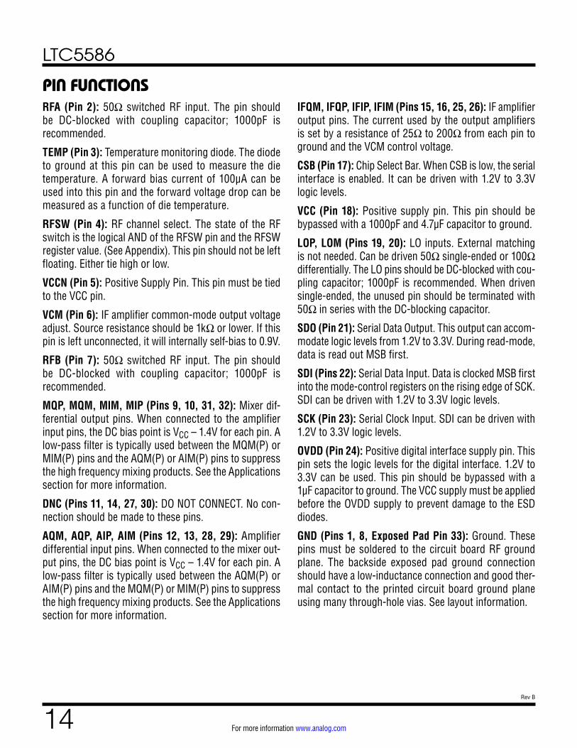
PIN FUNCTIONSRFA (Pin 2): 50Ω switched RF input. The pin should be DC-blocked with coupling capacitor; 1000pF is recommended.
TEMP (Pin 3): Temperature monitoring diode. The diode to ground at this pin can be used to measure the die temperature. A forward bias current of 100µA can be used into this pin and the forward voltage drop can be measured as a function of die temperature.
RFSW (Pin 4): RF channel select. The state of the RF switch is the logical AND of the RFSW pin and the RFSW register value. (See Appendix). This pin should not be left floating. Either tie high or low.
VCCN (Pin 5): Positive Supply Pin. This pin must be tied to the VCC pin.
VCM (Pin 6): IF amplifier common-mode output voltage adjust. Source resistance should be 1kΩ or lower. If this pin is left unconnected, it will internally self-bias to 0.9V.
RFB (Pin 7): 50Ω switched RF input. The pin should be DC-blocked with coupling capacitor; 1000pF is recommended.
MQP, MQM, MIM, MIP (Pins 9, 10, 31, 32): Mixer dif-ferential output pins. When connected to the amplifier input pins, the DC bias point is VCC – 1.4V for each pin. A low-pass filter is typically used between the MQM(P) or MIM(P) pins and the AQM(P) or AIM(P) pins to suppress the high frequency mixing products. See the Applications section for more information.
DNC (Pins 11, 14, 27, 30): DO NOT CONNECT. No con-nection should be made to these pins.
AQM, AQP, AIP, AIM (Pins 12, 13, 28, 29): Amplifier differential input pins. When connected to the mixer out-put pins, the DC bias point is VCC – 1.4V for each pin. A low-pass filter is typically used between the AQM(P) or AIM(P) pins and the MQM(P) or MIM(P) pins to suppress the high frequency mixing products. See the Applications section for more information.
IFQM, IFQP, IFIP, IFIM (Pins 15, 16, 25, 26): IF amplifier output pins. The current used by the output amplifiers is set by a resistance of 25Ω to 200Ω from each pin to ground and the VCM control voltage.
CSB (Pin 17): Chip Select Bar. When CSB is low, the serial interface is enabled. It can be driven with 1.2V to 3.3V logic levels.
VCC (Pin 18): Positive supply pin. This pin should be bypassed with a 1000pF and 4.7µF capacitor to ground.
LOP, LOM (Pins 19, 20): LO inputs. External matching is not needed. Can be driven 50Ω single-ended or 100Ω differentially. The LO pins should be DC-blocked with cou-pling capacitor; 1000pF is recommended. When driven single-ended, the unused pin should be terminated with 50Ω in series with the DC-blocking capacitor.
SDO (Pin 21): Serial Data Output. This output can accom-modate logic levels from 1.2V to 3.3V. During read-mode, data is read out MSB first.
SDI (Pins 22): Serial Data Input. Data is clocked MSB first into the mode-control registers on the rising edge of SCK. SDI can be driven with 1.2V to 3.3V logic levels.
SCK (Pin 23): Serial Clock Input. SDI can be driven with 1.2V to 3.3V logic levels.
OVDD (Pin 24): Positive digital interface supply pin. This pin sets the logic levels for the digital interface. 1.2V to 3.3V can be used. This pin should be bypassed with a 1µF capacitor to ground. The VCC supply must be applied before the OVDD supply to prevent damage to the ESD diodes.
GND (Pins 1, 8, Exposed Pad Pin 33): Ground. These pins must be soldered to the circuit board RF ground plane. The backside exposed pad ground connection should have a low-inductance connection and good ther-mal contact to the printed circuit board ground plane using many through-hole vias. See layout information.
APPLICATIONS INFORMATIONThe LTC5586 is an IQ demodulator designed for high dynamic range receiver applications. It consists of RF switches, a step attenuator, I/Q mixers, quadrature LO amplifiers, IF amplifiers, and correction circuitry for DC offset, image rejection, and non-linearity.
Operation
As shown in the Block Diagram for the LTC5586, the RF inputs, RFA and RFB, are selected by an internal switch. The RF signal is then converted to a differential signal by the on-chip balun transformer covering the 300MHz to 6GHz band. A differential 0 to 31dB step attenuator then scales the RF input level to the I and Q channel mixers.
The LO inputs are impedance matched using a program-mable network, and then accurately shifted in phase by 90° by an internal precision phase shifter. This phase shifter maintains the accurate quadrature relation over the full LO input range from 300MHz to 6GHz. In addi-tion, the phase shifter allows fine tuning of the phase difference between the I- and Q-channel LO with a resolu-tion of around 0.05 degrees to compensate for any phase mismatch between the mixers and phase mismatch intro-duced into the IF path by any filter component mismatch.
The differential mixer IF output signals are filtered off-chip to remove the fRF + fLO signal and other high frequency mixing products before being applied to the on-chip IF amplifiers. The IF amplifiers have adjustable gain and common-mode output voltage to allow for direct interfac-ing with A/D converters. The gain balance between both IF output channels of the LTC5586 can be fine tuned with
a resolution of about 0.016dB in order to compensate for gain mismatches in the IF signal path, either caused internally by the device or by external amplifiers and fil-ters. The DC offset in both IF channels can be adjusted in order to minimize the accumulated DC offset at the A/D converter input.
The RF switch state, attenuation, IF gain, gain error and phase error adjust, DC offset adjust, and non-linearity adjust registers are digitally controlled through a 4-wire SPI interface. The register map is detailed in the Appendix.
RF Input Ports
Figure 4 shows a simplified schematic of the demodula-tor’s RF inputs (the RFA input is identical to RFB input) which consist of an RF switch, balun transformer, and step-attenuator. External DC voltage should not be applied to the RF input pins. DC current flowing into the pins may cause damage to the chip. Series DC blocking capacitors should be used to couple the RF input pins to the RF sig-nal sources. The RF switch can be selected by the RFSW pin, and by the RFSW register 0x17 bit[0]. The RFA input is selected when the logical AND of the value of RFSW in register 0x17 and the logic level of the RFSW pin is 1 (see digital input pins section and register map). The switch state is detailed in Table 1.
Table 1. RF Switch State vs Logic LevelsRFSW
RegisterRFSW Pin
0 10 RFB RFB1 RFB RFA
C20.3pF
C11000pF
RFARFAINPUT
(MATCHED)
RFSWGND
VCC
RFB
5586 F04
LTC5586
Figure 4. Simplified Schematic of the RF Input with External Matching Components
As shown in Figure 5, the RF input ports are well matched with return loss greater than 10dB over the frequency range of 500MHz to 6GHz with a 0.3pF capacitor on C2. The RF pins can be externally matched over the 300MHz to 500MHz frequency range by changing C2 to 4.7pF. Figure 6 shows the RF input return loss with C2 set to 4.7pF. Table 2 shows the impedance and input reflec-tion coefficient for the RF input with C2 = 0.3pF. The input transmission line length is de-embedded from the measurement.
The demodulator’s LO input interface is shown in Figure 7. The input consists of a programmable input match and a high precision quadrature phase shifter which generates 0° and 90° phase shifted LO signals for the LO buffer amplifiers to drive the I/Q mixers. DC blocking capacitors are required on the LOP and LOM inputs. When using a
LTC5586
5586 F07
C50.3pF
C61000pF
C70.3pF
R149.9Ω
C81000pF
LOMATCHADJUST
0º
90º
GND
LOMLOINPUT
(MATCHED)
LOP
VCC
Figure 7. Simplified Schematic of the LO Inputs with Single-Ended Drive
Figure 8. Single-Ended LO Input Return Loss vs BAND, CF1, LF1, and CF2
0 1 2 3 4 5 6 7 8
5
0
–5
–10
–15
–20
–25
–30
–35
LO FREQUENCY (GHz)
–RET
URN
LOSS
(dB)
0, 31, 3, 310, 17, 2, 310, 14, 1, 271, 21, 3, 28
1, 15, 1, 311, 2, 1, 101, 1, 0, 191, 0, 0, 0
TC = 25°C
5586 F08
LTC5586
5586 F09
C50.3pF
C61000pF
C70.3pF
C81000pF
LOMATCHADJUST
0º
90º
GND
LOMLOINPUT
(MATCHED)
LOP
ANARENB4859A53
VCC
Figure 9. Simplified Schematic of the LO Inputs Using a Balun for Differential Drive
Figure 10. OIP2 vs Single-Ended and Differential LO Input
0 1 2 3 4 5 6
100
90
80
70
60
50
40
30
20
10
0
RF FREQUENCY (GHz)
OIP2
(dBm
)
I, SINGLE-ENDEDQ, SINGLE-ENDEDI, DIFFERENTIALQ, DIFFERENTIAL
5586 F10
TC = 25°C
The LO inputs can also be driven differentially. Figure 10 compares the uncalibrated OIP2 performance of single ended versus differential LO drive using the ANAREN B4859A53 balun as shown in the schematic of Figure 9.
An interstage IF filter should be used between the MIP (MIM) and AIP (AIM) pins and the MQP (MQM) and AQP (AQM) pins to suppress the large fRF + fLO and other mix-ing products from the mixer outputs. Without the filter, the linearity of the amplifier can be degraded for the desired signal. Figure 11 shows a recommended lowpass filter. Table 4 shows typical values used for a lowpass response of various bandwidths.
It is important that the placement of C10 and C12 be as close as possible to the amplifier inputs. Long line
lengths on the amplifier inputs can lead to instability. As shown in Figure 12, a 50Ω common-mode termination resistor can be used to better ensure stability with long line lengths and/or higher order filtering. The placement of C9 and C11 should be as close as possible to the mixer outputs for effective filtering of the 2xLO, fRF + fLO, and other mixing products.
By adjusting the values of the capacitors in the filter, it is possible to add or remove frequency slope of the IF
1pF
2k
42mA 42mA
1.5nH
1.5nH
0.2pF
0.2pF
L2
100Ω
0.6pF
50Ω
100Ω
50Ω50Ω
0.6pF
50Ω
L1
C11 C9
C12 C10
LTC5586
AC CURRENTSOURCE
PACKAGEPARASITICS
1.5nH
1.5nH
0.2pF
0.2pF
PACKAGEPARASITICS
VCC
GND
MIP
MIM
AIM
AIP
5586 F11
1pF
VCC
Figure 11. Simplified Schematic of the Mixer Output and IF Amplifier Input with Interstage Filter
Figure 12. Interstage IF Filter with Common-Mode Termination
APPLICATIONS INFORMATIONresponse. The RF input has a frequency slope above 2GHz of approximately –2dB/GHz. If a high-side LO (HSLO) is used the resulting IF slope will be 2dB/GHz. If a low-side LO (LSLO) is used the resulting IF slope will be –2dB/GHz. The IF filter component values can be adjusted so that approximately 1dB of peaking or roll-off can be achieved over the filter bandwidth to give an overall flat IF response for the HSLO or LSLO case.
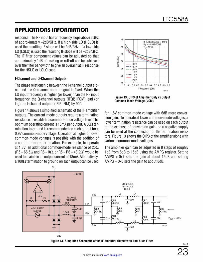
I-Channel and Q-Channel Outputs
The phase relationship between the I-channel output sig-nal and the Q-channel output signal is fixed. When the LO input frequency is higher (or lower) than the RF input frequency, the Q-channel outputs (IFQP, IFQM) lead (or lag) the I-channel outputs (IFIP, IFIM) by 90°.
Figure 14 shows a simplified schematic of the IF amplifier outputs. The current-mode outputs require a terminating resistance to establish a common-mode voltage level. The optimum operating current is 18mA per output. A 50Ω ter-mination to ground is recommended on each output for a 0.9V common-mode voltage. Operation at higher or lower common-mode voltages is possible with the addition of a common-mode termination. For example, to operate at 1.8V, an additional common-mode resistance of 25Ω (R5 = 66.5Ω and R6 = 0Ω, or R5 = R6 = 43.2Ω) would be used to maintain an output current of 18mA. Alternatively, a 100Ω termination to ground on each output can be used
for 1.8V common-mode voltage with 6dB more conver-sion gain. To operate at lower common-mode voltages, a lower termination resistance can be used on each output at the expense of conversion gain, or a negative supply can be used at the connection of the termination resis-tors. Figure 13 shows the OIP3 of the amplifier alone with various common-mode voltages.
The amplifier gain can be adjusted in 8 steps of roughly 1dB from 8dB to 15dB using the AMPG register. Setting AMPG = 0x7 sets the gain at about 15dB and setting AMPG = 0x0 sets the gain to about 8dB.
LTC5586
1.5nH
1.5nH
2k
0.2pF
0.2pF
L5
2k
L6
L7
L8
C17
C18
R224.9Ω
R368.1Ω
R468.1Ω
R50Ω
C21
C20C23
C24
R924.9Ω
R7200Ω
R8200Ω
R60Ω
AC CURRENTSOURCE
PACKAGEPARASITICS
IFIP
IFIM
VCM
GND
5TH ORDERANTI-ALIAS
FILTER
5586 F14
0.9V
0.9V
ZOUT = 100Ω
+–
VCC
Figure 14. Simplified Schematic of the IF Amplifier Output with Anti-Alias Filter
0 0.1 0.2 0.3 0.4 0.5 0.6 0.7 0.8 0.9 1.0
45
40
35
30
25
20
15
IF Frequency (GHz)
OIP3
(dBm
)
0.5V0.7V0.9V1.2V1.5V1.8V2.0V
IF TONESPACING = 1MHzPIF = –1.5dB/TONETC = 55°C
5586 F13
Figure 13. OIP3 of Amplifier Only vs Output Common-Mode Voltage (VCM)
APPLICATIONS INFORMATIONA typical anti-alias filter is shown in Figure 14 for inter-face with an ADC. The parallel combinations R3||R7 and R4||R8 set the differential impedance for the ADC. The input and output of the filter contain a common-mode ter-mination for high frequencies. These are formed by C17, C18 and 24.9Ω at the input and C23, C24 and 24.9Ω at the output. The common-mode termination at the ampli-fier output ensures stability and the common-mode ter-mination at the ADC input provides a termination for the high-frequency kickback from the sampling capacitors in the ADC. Table 5 shows some typical values vs 1dB cutoff frequency for the anti-alias filter. To optimize the flatness and ripple of the IF band, both the IF interstage filter and the anti-alias filter can be designed together in a simulator including package parasitics. The additional slope due to RF slope and HSLO or LSLO can be compensated by using this method. The layout of the anti-alias filter should be done so that the amplifier outputs and ADC inputs are as close as possible. This is to prevent long line lengths from introducing additional parasitics.
Table 5. Component Values for Anti-Alias Lowpass Filter1dB BW (MHz)
Table 6 and Table 7 show the differential and common-mode S-parameters for the amplifier by itself with 50Ω terminations on all ports. In addition, common-mode ter-minations were used on the input and output ports having a value of 2pF in series with 50Ω.
Table 6. IF Amplifier S-Parameters (Differential-Mode)IF
APPLICATIONS INFORMATIONAPPLICATIONS INFORMATIONThe common-mode feedback amplifier holds the com-mon-mode output voltage within about 20mV of the VCM pin voltage. The VCM pin interface is shown in Figure 15. The VCM pin should be driven by a voltage source with an output impedance lower than 1kΩ. When the VCM pin is unbiased, the output common-mode voltage will be held at a nominal 0.9V given by the internal voltage divider formed by the 40kΩ and 8kΩ resistors. Connecting the VCM pin to an ADC common-mode reference pin allows the output common-mode voltage of the IF amplifier to track the ADC common-mode.
Figure 15. Simplified Schematic of the VCM Input Pin
250Ω
40k
8k
6.5pF
20k
LTC5586
GND
VCM
5586 F15
VCC
100Ω
R2040.2k
LTC5586
GND
VTEMPTEMP
5586 F16
VCC VCC
Figure 16. Schematic of the TEMP Pin
Temperature Diode
A schematic of the TEMP pin is shown in Figure 16. The temperature diode can be used to directly measure the die temperature. A 40kΩ resistor is recommended to VCC to generate a 100µA current source for the diode readout. The temperature slope is about –1.52mV/°C.
Digital Input Pins
Figure 17 show the simplified schematics for the digital input pins, SCK, CSB, SDI, and RFSW. These pins should not be left floating, since there is no internal pull-down or pull-up.
2k
LTC5586
GND
DIGITALINPUT
5586 F17
VCC
Figure 17. Simplified Schematic of the Digital Input Pins (SCK, CSB, SDI, RFSW)
Figure 18. Simplified Schematic of the OVDD Pin Interface
LTC5586
GND
OVDD
DIGITALINPUTS
SDO
5586 F18
VCC
OVDD Interface
Figure 18 shows the simplified schematic of the OVDD interface. The OVDD pin supplies the voltage for the digital inputs and SDO pin. By setting the pin at 1.2V to 3.3V, the serial port can function with 1.2V to 3.3V logic levels. It is important that when sequencing the supply voltages for the chip that the VCC supply be brought up first before the OVDD supply. This is to prevent the ESD diode connected between OVDD and VCC from getting damaged.
Figure 19. Simplified Schematic of the SDO Pin Interface
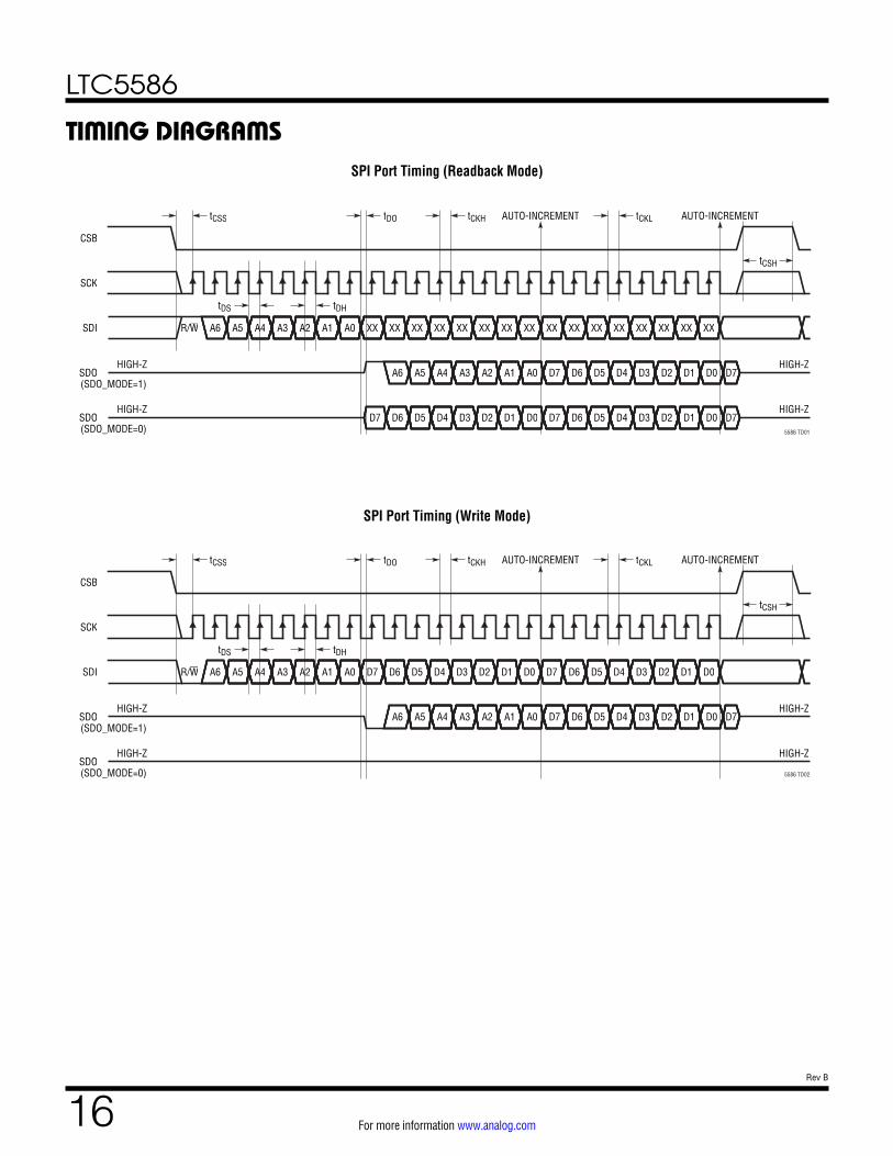
SERIAL PORT
The SPI-compatible serial port provides control and moni-toring functionality.
Communication Sequence
The serial bus is comprised of CSB, SCK, SDI and SDO. Data transfers to the part are accomplished by the serial bus master device first taking CSB low to enable the LTC5586’s port. Input data applied on SDI is clocked on the rising edge of SCK, with all transfers MSB first. The communication burst is terminated by the serial bus master returning CSB high. See the Timing Diagrams for details.
Data is read from the part during a communication burst using SDO. Readback may be multidrop (more than one LTC5586 or other serial device connected in parallel on the serial bus), as SDO is high impedance (Hi-Z) when CSB = 1.
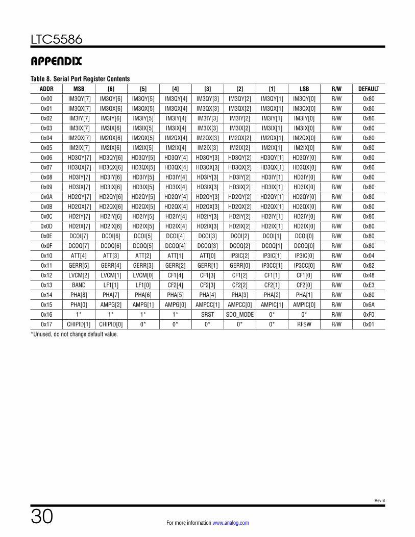
Single Byte Transfers
The serial port is arranged as a simple memory map, with status and control available in 23 registers as shown in the appendix. All data bursts are comprised of at least two 8-bit bytes. The most significant bit of the first byte is the read/write bit. Setting this bit to 1 puts the serial port into read mode. The next 7 bits of the first byte are address bits and can be set from 0x00 to 0x17. The subse-quent byte, or bytes, is data from/to the specified register address. See the Timing Diagrams for details. Note that the written data is transferred to the internal register at the falling edge of the 16th clock cycle (parallel load).
Multiple Byte Transfers
More efficient data transfer of multiple bytes is accom-plished by using the LTC5586’s register address auto-increment feature as shown in the Timing Diagrams. The serial port master sends the destination register address in the first byte and reads or writes data in the second byte as before, but on the third byte the address pointer is auto-incremented by 1 and the serial port master can read or write to subsequent registers. If the register address pointer attempts to increment past 23 (0x17), it is auto-matically reset to 0.
SDO_MODE Control Bit
The SDO output has two modes of operation as shown in the Timing Diagrams. When register 0x16 control bit SDO_MODE = 0, the SDO pin functions as a normal output which is High-Z during a write command. If SDO_MODE = 1, the SDO output is put into a serial repeater mode where SDO echoes the command written to SDI before readback of register contents either in read or write mode. This can be used in high bus noise environments where it is necessary to perform error-checking on commands sent to the serial port.
A simplified schematic of the SDO output is shown in Figure 19. The OVDD supply sets the logic level of the out-put, and a 25Ω series resistor limits the output current.
Register Defaults
The register map and defaults are given in Table 8 and 9 in the appendix. When the device is powered up, the reg-isters may not be reset to their default values. By writing a 1 to the SRST bit (bit[3]) of register 0x16, the device will go into soft reset and the registers will be reset to their default values.
Figure 20. Example Block Diagram of a DPD Transmitter with DSP for Impairment Minimization
[1] Saul Teukolsky, William T. Vetterling, William H. Press, and Brian P. Flannery, “Numerical Recipes in C: The Art of Scientific Computing,” p. 352, 1988.
Impairment Minimization
The LTC5586 contains circuitry for minimizing receiver impairments such as DC offset, Phase and Gain Error, and non-linearity. An example block diagram of a DPD transmitter application is shown in Figure 20. A DSP is used to implement a 2-tone source and minimization algo-rithms for calibration of impairments. To setup the DSP for impairment calibration, the DATA ENCODER would be configured to produce symbols for two tones in the band of interest. The tones would be modulated up to the carrier frequency of fLO before being applied to the LTC5586 RFA input. The tones are then down-converted to baseband for the DSP.
In the DSP, a complex-FFT can be used to extract gain error and phase error for image rejection optimization, while the FFT of each channel can be used to optimize DC offset and nonlinearities independently. One possible general optimization method would be to sequentially apply a 1-D minimization algorithm to each impairment. A simple bisection method or more complicated (but faster converging) Brent’s method[1] could be used for the 1-D minimization.
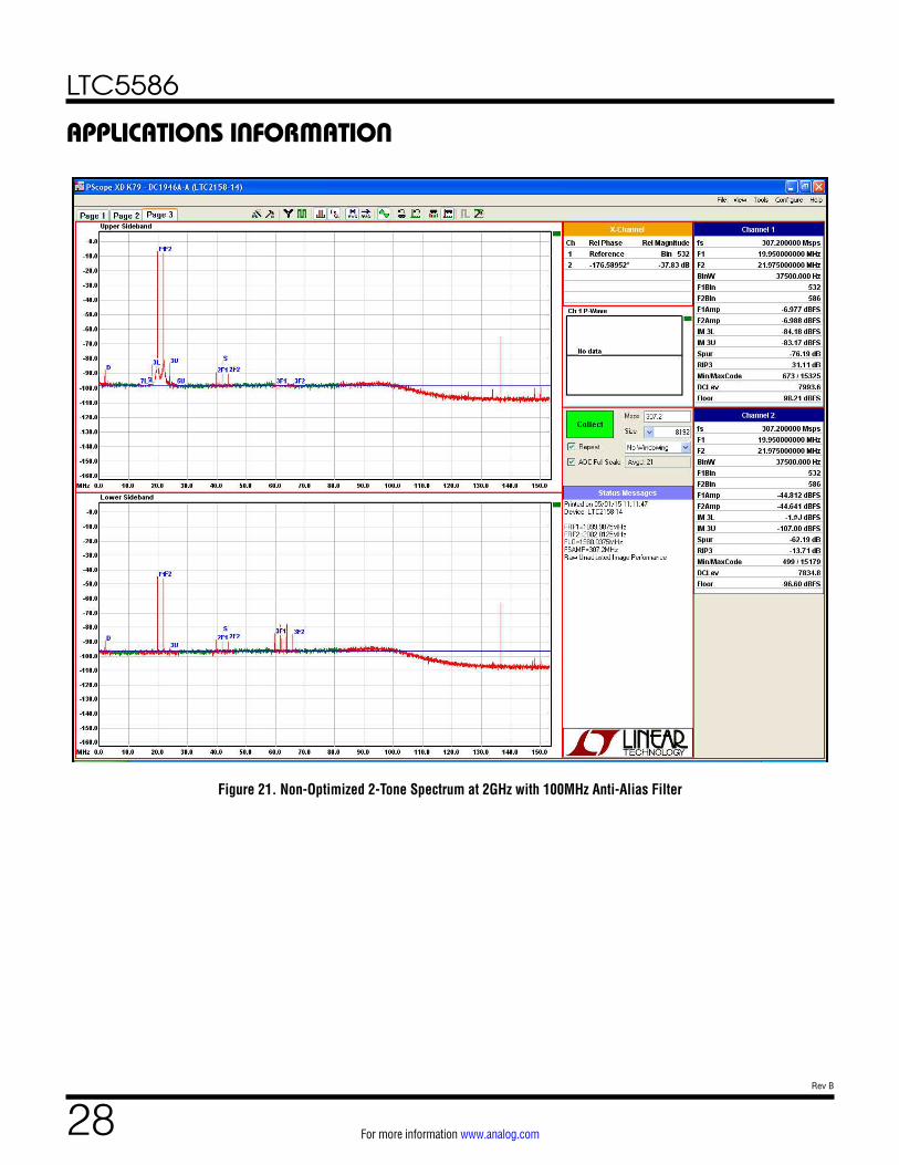
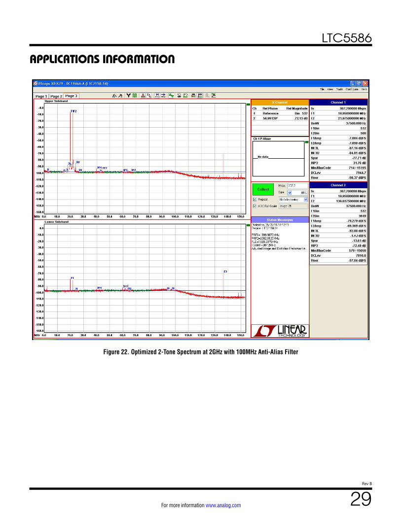
Figure 21 shows the non-optimized spectrum and Figure 22 shows the optimized spectrum for a 2-tone test signal at 2GHz. The Upper Sideband spectrum is the desired signal while the Lower Sideband is the image signal.
APPENDIXTable 9. Serial Port Register Bit Field SummaryBITS FUNCTION DESCRIPTION VALID VALUES DEFAULTAMPCC[1:0] IF Amplifier IM3 CC Adjust Used to optimize the IF amplifier IM3. 0x00 to 0x03 0x02AMPIC[1:0] IF Amplifier IM3 IC Adjust Used to optimize the IF amplifier IM3. 0x00 to 0x03 0x02AMPG[2:0] IF Amplifier Gain Adjust Adjusts the amplifier gain from 8dB to 15dB. 0x00 to 0x07 0x06ATT[4:0] Step Attenuator Control Controls the step attenuator from 0dB to 31dB attenuation. 0x00 to 0x1F 0x00BAND LO Band Select Selects which LO matching band is used. BAND = 1 for high band. BAND
= 0 for low band.0, 1 1
CF1[5:0] LO Matching Capacitor CF1 Controls the CF1 capacitor in the LO matching network. 0x00 to 0x1F 0x08CF2[5:0] LO Matching Capacitor CF2 Controls the CF2 capacitor in the LO matching network. 0x00 to 0x1F 0x03CHIPID Chip Identification Bits Factory set to default value. 0x00 to 0x03 0x00DCOI[7:0] I-Channel DC Offset Controls the I-channel DC offset over a range from –200mV to 200mV. 0x00 to 0xFF 0x80DCOQ[7:0] Q-Channel DC Offset Controls the Q-channel DC offset over a range from –200mV to 200mV. 0x00 to 0xFF 0x80GERR[5:0] IQ Gain Error Adjust Controls the IQ gain error over a range from –0.5dB to 0.5dB. 0x00 to 0x3F 0x20HD2IX[7:0] HD2 I-Channel X-Vector Controls the I-channel HD2 X-vector adjustment. 0x00 to 0xFF 0x80HD2IY[7:0] HD2 I-Channel Y-Vector Controls the I-channel HD2 Y-vector adjustment. 0x00 to 0xFF 0x80HD2QX[7:0] HD2 Q-Channel X-Vector Controls the Q-channel HD2 X-vector adjustment. 0x00 to 0xFF 0x80HD2QY[7:0] HD2 Q-Channel Y-Vector Controls the Q-channel HD2 Y-vector adjustment. 0x00 to 0xFF 0x80HD3IX[7:0] HD3 I-Channel X-Vector Controls the I-channel HD3 X-vector adjustment. 0x00 to 0xFF 0x80HD3IY[7:0] HD3 I-Channel Y-Vector Controls the I-channel HD3 Y-vector adjustment. 0x00 to 0xFF 0x80HD3QX[7:0] HD3 Q-Channel X-Vector Controls the Q-channel HD3 X-vector adjustment. 0x00 to 0xFF 0x80HD3QY[7:0] HD3 Q-Channel Y-Vector Controls the Q-channel HD3 Y-vector adjustment. 0x00 to 0xFF 0x80IM2IX[7:0] IM2 I-Channel X-Vector Controls the I-channel IM2 X-vector adjustment. 0x00 to 0xFF 0x80IM2QX[7:0] IM2 Q-Channel X-Vector Controls the Q-channel IM2 X-vector adjustment. 0x00 to 0xFF 0x80IM3IX[7:0] IM3 I-Channel X-Vector Controls the I-channel IM3 X-vector adjustment. 0x00 to 0xFF 0x80IM3IY[7:0] IM3 I-Channel Y-Vector Controls the I-channel IM3 Y-vector adjustment. 0x00 to 0xFF 0x80IM3QX[7:0] IM3 Q-Channel X-Vector Controls the Q-channel IM3 X-vector adjustment. 0x00 to 0xFF 0x80IM3QY[7:0] IM3 Q-Channel Y-Vector Controls the Q-channel IM3 Y-vector adjustment. 0x00 to 0xFF 0x80IP3CC[1:0] RF Input IP3 CC Adjust Used to optimize the RF input IP3. 0x00 to 0x03 0x02IP3IC[2:0] RF Input IP3 IC Adjust Used to optimize the RF input IP3. 0x00 to 0x07 0x04LF1[1:0] LO Matching Inductor LF1 Controls the LF1 inductor in the LO matching network. 0x00 to 0x03 0x03LVCM[2:0] LO Bias Adjust Used to optimize mixer IP3. 0x00 to 0x07 0x02PHA[8:0] IQ Phase Error Adjust Controls the IQ phase error over a range from –2.5 Degrees to 2.5
Degrees.0x000 to 0x1FF 0x100
RFSW RF Switch Input Select Controls the RF switch state with a logical AND of the RFSW pin. 0, 1 1SDO_MODE SDO Readback Mode Enables the SDO readback mode if SDO_MODE = 1. 0, 1 0SRST Soft Reset Writing 1 to this bit resets all registers to their default values. 0, 1 0
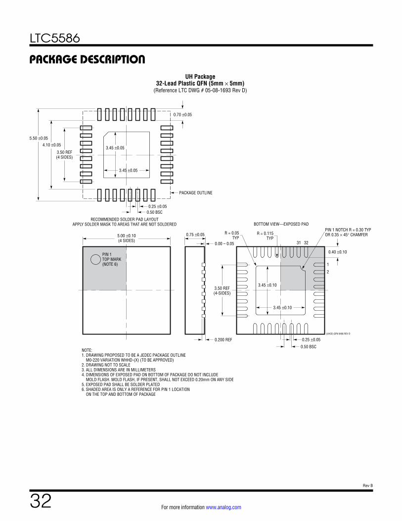
NOTE:1. DRAWING PROPOSED TO BE A JEDEC PACKAGE OUTLINE M0-220 VARIATION WHHD-(X) (TO BE APPROVED)2. DRAWING NOT TO SCALE3. ALL DIMENSIONS ARE IN MILLIMETERS4. DIMENSIONS OF EXPOSED PAD ON BOTTOM OF PACKAGE DO NOT INCLUDE MOLD FLASH. MOLD FLASH, IF PRESENT, SHALL NOT EXCEED 0.20mm ON ANY SIDE5. EXPOSED PAD SHALL BE SOLDER PLATED6. SHADED AREA IS ONLY A REFERENCE FOR PIN 1 LOCATION ON THE TOP AND BOTTOM OF PACKAGE
PIN 1TOP MARK(NOTE 6)
0.40 ±0.10
31
1
2
32
BOTTOM VIEW—EXPOSED PAD
3.50 REF(4-SIDES)
3.45 ±0.10
3.45 ±0.10
0.75 ±0.05 R = 0.115TYP
0.25 ±0.05(UH32) QFN 0406 REV D
0.50 BSC
0.200 REF
0.00 – 0.05
0.70 ±0.05
3.50 REF(4 SIDES)
4.10 ±0.05
5.50 ±0.05
0.25 ±0.05
PACKAGE OUTLINE
0.50 BSC
RECOMMENDED SOLDER PAD LAYOUTAPPLY SOLDER MASK TO AREAS THAT ARE NOT SOLDERED
Information furnished by Analog Devices is believed to be accurate and reliable. However, no responsibility is assumed by Analog Devices for its use, nor for any infringements of patents or other rights of third parties that may result from its use. Specifications subject to change without notice. No license is granted by implication or otherwise under any patent or patent rights of Analog Devices.
For more information www.analog.com ANALOG DEVICES, INC. 2017 to 2018
D16966-0-7/18(B)www.analog.com
RELATED PARTS
TYPICAL APPLICATION
PART NUMBER DESCRIPTION COMMENTSInfrastructureLTC5569 300MHz to 4GHz Dual Active Downconverting
Mixer2dB Gain, 26.7dBm IIP3 and 11.7dB NF at 1950MHz, 3.3V/180mA Supply
LTC6409 10GHz GBW Differential Amplifier DC-Coupled, 48dBm OIP3 at 140MHz, 1.1nV/√Hz Input Noise DensityLTC5549 2GHz to 14GHz Mixer with Integrated LO Doubler Ultra-Wideband Bidirectional Up-, or Down-Conversion Mixer, +22.8dBm IIP3 at
12GHz, 0dBm LO Drive, 500MHz to 6GHz IF BandwidthLTC5548 2GHz to 14GHz Mixer with IF Frequency Extending
to DCUltra-Wideband Bidirectional Up-, or Down-Conversion Mixer, +18.7dBm IIP3 at 12GHz, 0dBm LO Drive with On-Chip Frequency Doubler, DC to 6GHz IF Bandwidth
LTC5588-1 200MHz to 6GHz Quadrature Modulator +31dBm OIP3, –160dBm/Hz Output Noise Floor, Excellent ACPR PerformanceRF PLL/Synthesizer with VCOLTC6946-3 Low Noise, Low Spurious Integer-N PLL with