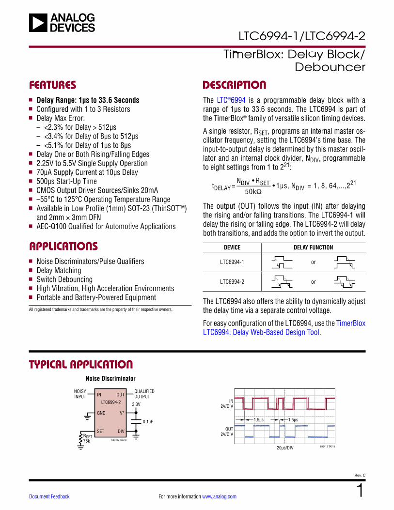
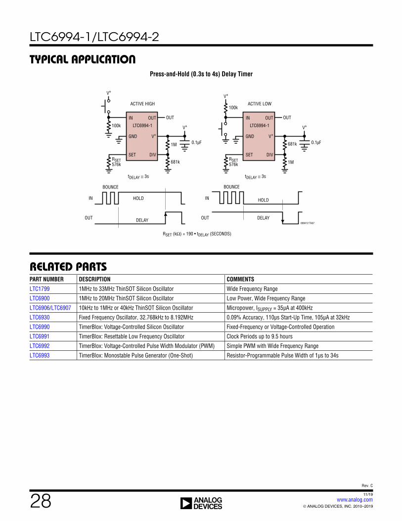
LTC6994-1/LTC6994-2 1 Rev. C For more information www.analog.com TYPICAL APPLICATION FEATURES DESCRIPTION TimerBlox: Delay Block/ Debouncer The LTC ® 6994 is a programmable delay block with a range of 1µs to 33.6 seconds. The LTC6994 is part of the TimerBlox ® family of versatile silicon timing devices. A single resistor, R SET , programs an internal master os- cillator frequency, setting the LTC6994’s time base. The input-to-output delay is determined by this master oscil- lator and an internal clock divider, N DIV , programmable to eight settings from 1 to 2 21 : t DELAY = N DIV •R SET 50kΩ • 1µs, N DIV = 1, 8, 64,...,2 21 The output (OUT) follows the input (IN) after delaying the rising and/or falling transitions. The LTC6994-1 will delay the rising or falling edge. The LTC6994-2 will delay both transitions, and adds the option to invert the output. DEVICE DELAY FUNCTION LTC6994-1 or LTC6994-2 or The LTC6994 also offers the ability to dynamically adjust the delay time via a separate control voltage. For easy configuration of the LTC6994, use the TimerBlox LTC6994: Delay Web-Based Design Tool. Noise Discriminator APPLICATIONS n Delay Range: 1µs to 33.6 Seconds n Configured with 1 to 3 Resistors n Delay Max Error: – <2.3% for Delay > 512µs – <3.4% for Delay of 8µs to 512µs – <5.1% for Delay of 1µs to 8µs n Delay One or Both Rising/Falling Edges n 2.25V to 5.5V Single Supply Operation n 70µA Supply Current at 10µs Delay n 500µs Start-Up Time n CMOS Output Driver Sources/Sinks 20mA n –55°C to 125°C Operating Temperature Range n Available in Low Profile (1mm) SOT-23 (ThinSOT™) and 2mm × 3mm DFN n AEC-Q100 Qualified for Automotive Applications n Noise Discriminators/Pulse Qualifiers n Delay Matching n Switch Debouncing n High Vibration, High Acceleration Environments n Portable and Battery-Powered Equipment All registered trademarks and trademarks are the property of their respective owners. 699412 TA01a LTC6994-2 OUT V + DIV IN GND SET R SET 75k 3.3V 0.1μF NOISY INPUT QUALIFIED OUTPUT IN 2V/DIV OUT 2V/DIV 20μs/DIV 699412 TA01b 1.5μs 1.5μs Document Feedback
Transcript
LTC6994-1/LTC6994-2
1Rev. C
For more information www.analog.com
TYPICAL APPLICATION
FEATURES DESCRIPTION
TimerBlox: Delay Block/ Debouncer
The LTC®6994 is a programmable delay block with a range of 1µs to 33.6 seconds. The LTC6994 is part of the TimerBlox® family of versatile silicon timing devices.
A single resistor, RSET , programs an internal master os-cillator frequency, setting the LTC6994’s time base. The input-to-output delay is determined by this master oscil-lator and an internal clock divider, NDIV , programmable to eight settings from 1 to 221:
tDELAY =
NDIV • RSET50kΩ
• 1µs, NDIV = 1, 8, 64,...,221
The output (OUT) follows the input (IN) after delaying the rising and/or falling transitions. The LTC6994-1 will delay the rising or falling edge. The LTC6994-2 will delay both transitions, and adds the option to invert the output.
DEVICE DELAY FUNCTION
LTC6994-1 or
LTC6994-2 or
The LTC6994 also offers the ability to dynamically adjust the delay time via a separate control voltage.
For easy configuration of the LTC6994, use the TimerBlox LTC6994: Delay Web-Based Design Tool.
Noise Discriminator
APPLICATIONS
n Delay Range: 1µs to 33.6 Secondsn Configured with 1 to 3 Resistorsn Delay Max Error: – <2.3% for Delay > 512µs – <3.4% for Delay of 8µs to 512µs – <5.1% for Delay of 1µs to 8µsn Delay One or Both Rising/Falling Edgesn 2.25V to 5.5V Single Supply Operationn 70µA Supply Current at 10µs Delayn 500µs Start-Up Timen CMOS Output Driver Sources/Sinks 20mAn –55°C to 125°C Operating Temperature Rangen Available in Low Profile (1mm) SOT-23 (ThinSOT™) and 2mm × 3mm DFNn AEC-Q100 Qualified for Automotive Applications
n Noise Discriminators/Pulse Qualifiersn Delay Matchingn Switch Debouncingn High Vibration, High Acceleration Environmentsn Portable and Battery-Powered EquipmentAll registered trademarks and trademarks are the property of their respective owners.
ABSOLUTE MAXIMUM RATINGSSupply Voltage (V+) to GND ........................................6VMaximum Voltage on Any Pin.................................. (GND – 0.3V) ≤ VPIN ≤ (V+ + 0.3V)Operating Temperature Range (Note 2)
LTC6994C ............................................–40°C to 85°C LTC6994I .............................................–40°C to 85°C LTC6994H .......................................... –40°C to 125°C LTC6994MP ....................................... –55°C to 125°C
(Note 1)
ORDER INFORMATIONLead Free FinishTAPE AND REEL (MINI) TAPE AND REEL PART MARKING PACKAGE DESCRIPTION SPECIFIED TEMPERATURE RANGELTC6994CDCB-1#TRMPBF LTC6994CDCB-1#TRPBF LFCT 6-Lead (2mm x 3mm) Plastic DFN 0°C to 70°CLTC6994IDCB-1#TRMPBF LTC6994IDCB-1#TRPBF LFCT 6-Lead (2mm x 3mm) Plastic DFN –40°C to 85°CLTC6994HDCB-1#TRMPBF LTC6994HDCB-1#TRPBF LFCT 6-Lead (2mm x 3mm) Plastic DFN –40°C to 125°CLTC6994CS6-1#TRMPBF LTC6994CS6-1#TRPBF LTFCV 6-Lead Plastic TSOT-23 0°C to 70°CLTC6994IS6-1#TRMPBF LTC6994IS6-1#TRPBF LTFCV 6-Lead Plastic TSOT-23 –40°C to 85°CLTC6994HS6-1#TRMPBF LTC6994HS6-1#TRPBF LTFCV 6-Lead Plastic TSOT-23 –40°C to 125°CLTC6994CDCB-2#TRMPBF LTC6994CDCB-2#TRPBF LFCW 6-Lead (2mm x 3mm) Plastic DFN 0°C to 70°CLTC6994IDCB-2#TRMPBF LTC6994IDCB-2#TRPBF LFCW 6-Lead (2mm x 3mm) Plastic DFN –40°C to 85°CLTC6994HDCB-2#TRMPBF LTC6994HDCB-2#TRPBF LFCW 6-Lead (2mm x 3mm) Plastic DFN –40°C to 125°CLTC6994CS6-2#TRMPBF LTC6994CS6-2#TRPBF LTFCX 6-Lead Plastic TSOT-23 0°C to 70°CLTC6994IS6-2#TRMPBF LTC6994IS6-2#TRPBF LTFCX 6-Lead Plastic TSOT-23 –40°C to 85°CLTC6994HS6-2#TRMPBF LTC6994HS6-2#TRPBF LTFCX 6-Lead Plastic TSOT-23 –40°C to 125°CLTC6994MPS6-1#TRMPBF LTC6994MPS6-1#TRPBF LTFCV 6-Lead Plastic TSOT-23 –55°C to 125°CLTC6994MPS6-2#TRMPBF LTC6994MPS6-2#TRPBF LTFCX 6-Lead Plastic TSOT-23 –55°C to 125°C
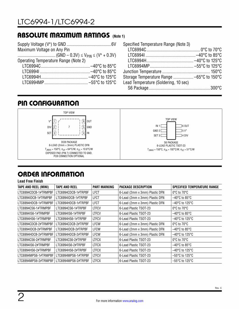
TOP VIEW
OUT
GND
IN
V+
DIV
SET
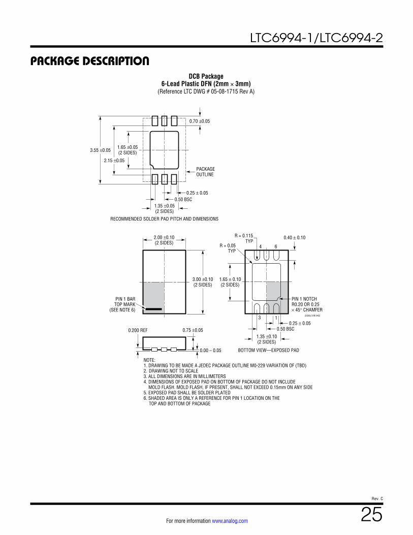
DCB PACKAGE6-LEAD (2mm × 3mm) PLASTIC DFN
4
57
6
3
2
1
TJMAX = 150°C, θJA = 64°C/W, θJC = 10.6°C/WEXPOSED PAD (PIN 7) CONNECTED TO GND,
PCB CONNECTION OPTIONAL
IN 1
GND 2
SET 3
6 OUT
5 V+
4 DIV
TOP VIEW
S6 PACKAGE6-LEAD PLASTIC TSOT-23
TJMAX = 150°C, θJA = 192°C/W, θJC = 51°C/W
PIN CONFIGURATION
Specified Temperature Range (Note 3) LTC6994C ................................................ 0°C to 70°C LTC6994I .............................................–40°C to 85°C LTC6994H .......................................... –40°C to 125°C LTC6994MP ....................................... –55°C to 125°C
Junction Temperature ........................................... 150°CStorage Temperature Range .................. –65°C to 150°CLead Temperature (Soldering, 10 sec) S6 Package ....................................................... 300°C
ORDER INFORMATIONLead Free FinishAUTOMOTIVE PRODUCTS**
TAPE AND REEL (MINI) TAPE AND REEL PART MARKING PACKAGE DESCRIPTION SPECIFIED TEMPERATURE RANGELTC6994IS6-1#WTRMPBF LTC6994IS6-1#WTRPBF LTFCV 6-Lead Plastic TSOT-23 –40°C to 85°CLTC6994HS6-1#WTRMPBF LTC6994HS6-1#WTRPBF LTFCV 6-Lead Plastic TSOT-23 –40°C to 125°CLTC6994IS6-2#WTRMPBF LTC6994IS6-2#WTRPBF LTFCX 6-Lead Plastic TSOT-23 –40°C to 85°CLTC6994HS6-2#WTRMPBF LTC6994HS6-2#WTRPBF LTFCX 6-Lead Plastic TSOT-23 –40°C to 125°C
Contact the factory for parts specified with wider operating temperature ranges. *The temperature grade is identified by a label on the shipping container.
Tape and reel specifications. Some packages are available in 500 unit reels through designated sales channels with #TRMPBF suffix.**Versions of this part are available with controlled manufacturing to support the quality and reliability requirements of automotive applications. These
models are designated with a #W suffix. Only the automotive grade products shown are available for use in automotive applications. Contact your local Analog Devices account representative for specific product ordering information and to obtain the specific Automotive Reliability reports for these models.
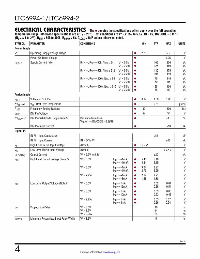
ELECTRICAL CHARACTERISTICS The l denotes the specifications which apply over the full operating temperature range, otherwise specifications are at TA = 25°C. Test conditions are V+ = 2.25V to 5.5V, IN = 0V, DIVCODE = 0 to 15 (NDIV = 1 to 221), RSET = 50k to 800k, RLOAD = 5k, CLOAD = 5pF unless otherwise noted.
SYMBOL PARAMETER CONDITIONS MIN TYP MAX UNITS
tDELAY Delay Time 1µ 33.55 sec
∆tDELAY Delay Accuracy (Note 4) NDIV ≥ 512
l
±1.7 ±2.3 ±3.0
% %
8 ≤ NDIV ≤ 64
l
±2.4 ±3.4 ±4.4
% %
NDIV = 1
l
±3.8 ±5.1 ±6.2
% %
∆tDELAY/∆T Delay Drift Over Temperature NDIV ≥ 512 NDIV ≤ 64
l
l
±0.006 ±0.008
%/°C %/°C
Delay Change With Supply NDIV ≥ 512 V+ = 4.5V to 5.5V V+ = 2.25V to 4.5V
l
l
–0.6 –0.4
–0.2 –0.1
% %
8 ≤ NDIV ≤ 64 V+ = 4.5V to 5.5V V+ = 2.7V to 4.5V V+ = 2.25V to 2.7V
ELECTRICAL CHARACTERISTICS The l denotes the specifications which apply over the full operating temperature range, otherwise specifications are at TA = 25°C. Test conditions are V+ = 2.25V to 5.5V, IN = 0V, DIVCODE = 0 to 15 (NDIV = 1 to 221), RSET = 50k to 800k, RLOAD = 5k, CLOAD = 5pF unless otherwise noted.
Note 1: Stresses beyond those listed under Absolute Maximum Ratings may cause permanent damage to the device. Exposure to any Absolute Maximum Rating condition for extended periods may affect device reliability and lifetime.Note 2: The LTC6994C is guaranteed functional over the operating temperature range of –40°C to 85°C.Note 3: The LTC6994C is guaranteed to meet specified performance from 0°C to 70°C. The LTC6994C is designed, characterized and expected to meet specified performance from –40°C to 85°C but it is not tested or QA sampled at these temperatures. The LTC6994I is guaranteed to meet specified performance from –40°C to 85°C. The LTC6994H is guaranteed to meet specified performance from –40°C to 125°C. The LTC6994MP is guaranteed to meet specified performance from –55°C to 125°C.Note 4: Delay accuracy is defined as the deviation from the tDELAY equation, assuming RSET is used to program the delay.
ELECTRICAL CHARACTERISTICS The l denotes the specifications which apply over the full operating temperature range, otherwise specifications are at TA = 25°C. Test conditions are V+ = 2.25V to 5.5V, IN = 0V, DIVCODE = 0 to 15 (NDIV = 1 to 221), RSET = 50k to 800k, RLOAD = 5k, CLOAD = 5pF unless otherwise noted.
Note 5: See Operation section, Table 1 and Figure 2 for a full explanation of how the DIV pin voltage selects the value of DIVCODE.Note 6: The IN pin has hysteresis to accommodate slow rising or falling signals. The threshold voltages are proportional to V+. Typical values can be estimated at any supply voltage using: VIN(RISING) ≈ 0.55 • V+ + 185mV and VIN(FALLING) ≈ 0.48 • V+ – 155mVNote 7: To conform to the Logic IC Standard, current out of a pin is arbitrarily given a negative value.Note 8: Output rise and fall times are measured between the 10% and the 90% power supply levels with 5pF output load. These specifications are based on characterization.Note 9: Settling time is the amount of time required for the output to settle within ±1% of the final delay after a 0.5× or 2× change in ISET .Note 10: Jitter is the ratio of the deviation of the programmed delay to the mean of the delay. This specification is based on characterization and is not 100% tested.
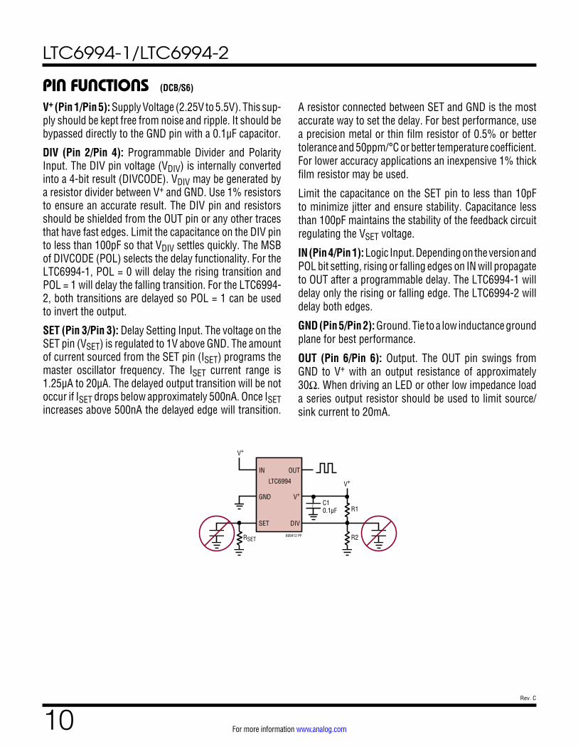
V+ (Pin 1/Pin 5): Supply Voltage (2.25V to 5.5V). This sup-ply should be kept free from noise and ripple. It should be bypassed directly to the GND pin with a 0.1µF capacitor.
DIV (Pin 2/Pin 4): Programmable Divider and Polarity Input. The DIV pin voltage (VDIV) is internally converted into a 4-bit result (DIVCODE). VDIV may be generated by a resistor divider between V+ and GND. Use 1% resistors to ensure an accurate result. The DIV pin and resistors should be shielded from the OUT pin or any other traces that have fast edges. Limit the capacitance on the DIV pin to less than 100pF so that VDIV settles quickly. The MSB of DIVCODE (POL) selects the delay functionality. For the LTC6994-1, POL = 0 will delay the rising transition and POL = 1 will delay the falling transition. For the LTC6994-2, both transitions are delayed so POL = 1 can be used to invert the output.
SET (Pin 3/Pin 3): Delay Setting Input. The voltage on the SET pin (VSET) is regulated to 1V above GND. The amount of current sourced from the SET pin (ISET) programs the master oscillator frequency. The ISET current range is 1.25µA to 20µA. The delayed output transition will be not occur if ISET drops below approximately 500nA. Once ISET increases above 500nA the delayed edge will transition.
A resistor connected between SET and GND is the most accurate way to set the delay. For best performance, use a precision metal or thin film resistor of 0.5% or better tolerance and 50ppm/°C or better temperature coefficient. For lower accuracy applications an inexpensive 1% thick film resistor may be used.
Limit the capacitance on the SET pin to less than 10pF to minimize jitter and ensure stability. Capacitance less than 100pF maintains the stability of the feedback circuit regulating the VSET voltage.
IN (Pin 4/Pin 1): Logic Input. Depending on the version and POL bit setting, rising or falling edges on IN will propagate to OUT after a programmable delay. The LTC6994-1 will delay only the rising or falling edge. The LTC6994-2 will delay both edges.
GND (Pin 5/Pin 2): Ground. Tie to a low inductance ground plane for best performance.
OUT (Pin 6/Pin 6): Output. The OUT pin swings from GND to V+ with an output resistance of approximately 30Ω. When driving an LED or other low impedance load a series output resistor should be used to limit source/sink current to 20mA.
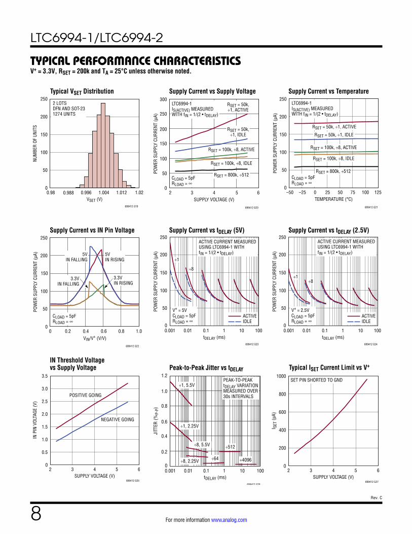
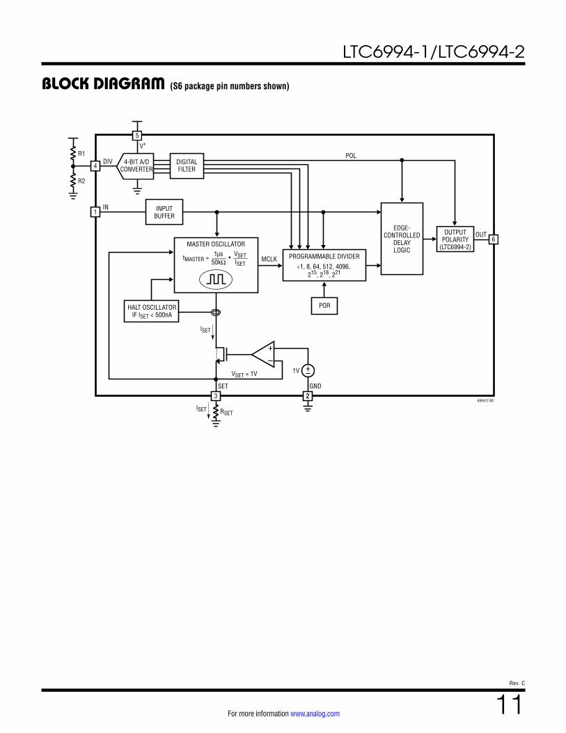
OPERATIONThe LTC6994 is built around a master oscillator with a 1µs minimum period. The oscillator is controlled by the SET pin current (ISET) and voltage (VSET), with a 1µs/50kΩ conversion factor that is accurate to ±1.7% under typical conditions.
tMASTER =
1µs50kΩ
•VSETISET
A feedback loop maintains VSET at 1V ±30mV, leaving ISET as the primary means of controlling the input-to-output delay. The simplest way to generate ISET is to connect a resistor (RSET) between SET and GND, such that ISET = VSET/RSET . The master oscillator equation reduces to:
tMASTER = 1µs •
RSET50kΩ
From this equation, it is clear that VSET drift will not affect the input-to-output delay when using a single program resistor (RSET). Error sources are limited to RSET toler-ance and the inherent accuracy ∆tDELAY of the LTC6994.
RSET may range from 50k to 800k (equivalent to ISET between 1.25µA and 20µA).
When the input makes a transition that will be delayed (as determined by the part version and POL bit setting), the master oscillator is enabled to time the delay. When the desired duration is reached, the output is allowed to transition.
The LTC6994 also includes a programmable frequency divider which can further divide the frequency by 1, 8, 64, 512, 4096, 215, 218 or 221. This extends the delay duration by those same factors. The divider ratio NDIV is set by a resistor divider attached to the DIV pin.
tDELAY =
NDIV50kΩ
•VSETISET
• 1µs
With RSET in place of VSET/ISET the equation reduces to:
tDELAY =
NDIV •RSET50kΩ
• 1µs
DIVCODE
The DIV pin connects to an internal, V+ referenced 4-bit A/D converter that determines the DIVCODE value. DIVCODE programs two settings on the LTC6994:
1. DIVCODE determines the frequency divider setting, NDIV .
2. The DIVCODE MSB is the POL bit, and configures a different polarity setting on the two versions.
a. LTC6994-1: POL selects rising or falling-edge delays. POL = 0 will delay rising-edge transitions. POL = 1 will delay falling-edge transitions.
b. LTC6994-2: POL selects the output inversion. POL = 1 inverts the output signal.
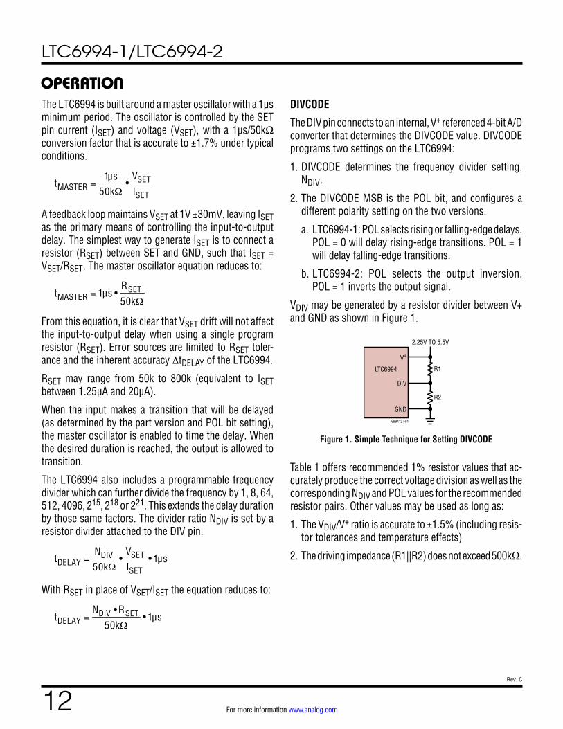
VDIV may be generated by a resistor divider between V+ and GND as shown in Figure 1.
699412 F01
LTC6994
V+
DIV
GND
R1
R2
2.25V TO 5.5V
Figure 1. Simple Technique for Setting DIVCODE
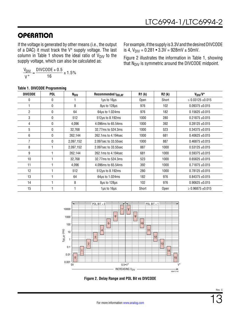
Table 1 offers recommended 1% resistor values that ac-curately produce the correct voltage division as well as the corresponding NDIV and POL values for the recommended resistor pairs. Other values may be used as long as:
1. The VDIV/V+ ratio is accurate to ±1.5% (including resis-tor tolerances and temperature effects)
2. The driving impedance (R1||R2) does not exceed 500kΩ.
4 0 4,096 4.096ms to 65.54ms 1000 392 0.28125 ±0.015
5 0 32,768 32.77ms to 524.3ms 1000 523 0.34375 ±0.015
6 0 262,144 262.1ms to 4.194sec 1000 681 0.40625 ±0.015
7 0 2,097,152 2.097sec to 33.55sec 1000 887 0.46875 ±0.015
8 1 2,097,152 2.097sec to 33.55sec 887 1000 0.53125 ±0.015
9 1 262,144 262.1ms to 4.194sec 681 1000 0.59375 ±0.015
10 1 32,768 32.77ms to 524.3ms 523 1000 0.65625 ±0.015
11 1 4,096 4.096ms to 65.54ms 392 1000 0.71875 ±0.015
12 1 512 512µs to 8.192ms 280 1000 0.78125 ±0.015
13 1 64 64µs to 1.024ms 182 976 0.84375 ±0.015
14 1 8 8µs to 128µs 102 976 0.90625 ±0.015
15 1 1 1µs to 16µs Short Open ≥ 0.96875 ±0.015
Figure 2. Delay Range and POL Bit vs DIVCODE
If the voltage is generated by other means (i.e., the output of a DAC) it must track the V+ supply voltage. The last column in Table 1 shows the ideal ratio of VDIV to the supply voltage, which can also be calculated as:
VDIV
V +=
DIVCODE + 0.516
± 1.5%
For example, if the supply is 3.3V and the desired DIVCODE is 4, VDIV = 0.281 • 3.3V = 928mV ± 50mV.
Figure 2 illustrates the information in Table 1, showing that NDIV is symmetric around the DIVCODE midpoint.
Figure 3. Rising-Edge Delayed Timing Diagram (LTC6994-1, POL = 0)
Figure 4. Falling-Edge Delayed Timing Diagram (LTC6994-1, POL = 1)
Edge-Controlled Delay
The LTC6994 is a programmable delay or pulse qualifier. It can perform noise filtering, which distinguishes it from a delay line (which simply delays all input transitions).
When the voltage on the LTC6994 input pin (IN) transitions low or high, the LTC6994 can delay the corresponding output transition by any time from 1µs to 33.6 seconds.
LTC6994-1 Functionality
Figures 3 details the basic operation of the LTC6994-1 when configured to delay rising edge transitions (POL = 0). A rising edge on the IN pin initiates the timing. OUT remains
low for the duration of tDELAY . If IN stays high then OUT will transition high after this time. If the input doesn’t remain high long enough for OUT to transition high then the timing will restart on each successive rising edge. In this way, the LTC6994-1 can serve as a pulse qualifier, filtering out noisy or short signals.
On a falling edge at the input, the output will follow im-mediately (after a short propagation delay tPD).Note that the output pulse width may be extremely short if IN falls immediately after OUT rises.
Figure 4 details the operation of the LTC6994-1 when configured to delay falling edges (POL = 1).
Figures 5 details the basic operation of the LTC6994-2 when configured for noninverting operation (POL = 0). As before, a rising edge on the IN pin initiates the timing and, if IN remains high, OUT will transition high after tDELAY .
Unlike the LTC6994-1, falling edges are delayed in the same way. When IN transitions low, OUT will follow after tDELAY .
If the input doesn’t remain high or low long enough for OUT to follow, the timing will restart on the next transition.
Also unlike the LTC6994-1, the output pulse width can never be less than tDELAY . Therefore, the LTC6994-2 can generate pulses with a defined minimum width.
Figure 6 details the operation of the LTC6994-2 when the output is inverted (POL = 1).
Figure 5. Both Edges Delayed Timing Diagram (LTC6994-2, POL = 0)
Figure 6. Both Edges Delayed (Inverting) Timing Diagram (LTC6994-2, POL = 1)
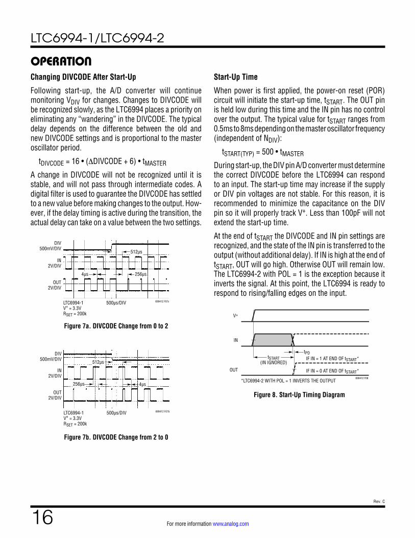
Following start-up, the A/D converter will continue monitoring VDIV for changes. Changes to DIVCODE will be recognized slowly, as the LTC6994 places a priority on eliminating any “wandering” in the DIVCODE. The typical delay depends on the difference between the old and new DIVCODE settings and is proportional to the master oscillator period.
tDIVCODE = 16 • (∆DIVCODE + 6) • tMASTER
A change in DIVCODE will not be recognized until it is stable, and will not pass through intermediate codes. A digital filter is used to guarantee the DIVCODE has settled to a new value before making changes to the output. How-ever, if the delay timing is active during the transition, the actual delay can take on a value between the two settings.
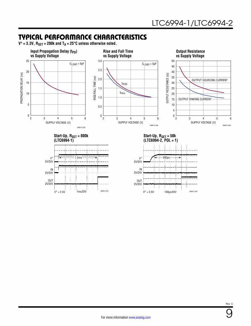
Start-Up Time
When power is first applied, the power-on reset (POR) circuit will initiate the start-up time, tSTART . The OUT pin is held low during this time and the IN pin has no control over the output. The typical value for tSTART ranges from 0.5ms to 8ms depending on the master oscillator frequency (independent of NDIV):
tSTART(TYP) = 500 • tMASTER
During start-up, the DIV pin A/D converter must determine the correct DIVCODE before the LTC6994 can respond to an input. The start-up time may increase if the supply or DIV pin voltages are not stable. For this reason, it is recommended to minimize the capacitance on the DIV pin so it will properly track V+. Less than 100pF will not extend the start-up time.
At the end of tSTART the DIVCODE and IN pin settings are recognized, and the state of the IN pin is transferred to the output (without additional delay). If IN is high at the end of tSTART, OUT will go high. Otherwise OUT will remain low. The LTC6994-2 with POL = 1 is the exception because it inverts the signal. At this point, the LTC6994 is ready to respond to rising/falling edges on the input.
The simplest and most accurate method to program the LTC6994 is to use a single resistor, RSET , between the SET and GND pins. The design procedure is a 3-step process. Alternatively, Linear Technology offers the easy-to-use TimerBlox Designer tool to quickly design any LTC6994 based circuit. Use the free TimerBlox LTC6994: Delay Web-Based Design Tool.
Step 1: Select the LTC6994 Version and POL Bit Setting.
Choose LTC6994-1 to delay one (rising or falling) input transition. The POL bit then defines which edge is to be delayed. POL = 0 delays rising edges. POL = 1 delays falling edges.
Choose LTC6994-2 to delay rising and falling edges. Set POL = 0 for normal operation, or POL = 1 to invert the output.
Step 2: Select the NDIV Frequency Divider Value.
As explained earlier, the voltage on the DIV pin sets the DIVCODE which determines both the POL bit and the NDIV value. For a given delay time (tDELAY), NDIV should be selected to be within the following range:
tDELAY16µs
≤ NDIV ≤tDELAY
1µs (1)
To minimize supply current, choose the lowest NDIV value. However, in some cases a higher value for NDIV will provide better accuracy (see Electrical Characteristics).
Table 1 can also be used to select the appropriate NDIV values for the desired tDELAY .
With POL already chosen, this completes the selection of DIVCODE. Use Table 1 to select the proper resistor divider or VDIV/V+ ratio to apply to the DIV pin.
Step 3: Calculate and Select RSET .
The final step is to calculate the correct value for RSET using the following equation:
RSET =
50k1µs
•tDELAYNDIV
(2)
Select the standard resistor value closest to the calculated value.
Example: Design a circuit to delay falling edges by tDELAY = 100µs with minimum power consumption.
Step 1: Select the LTC6994 Version and POL Bit Setting.
To delay negative transitions, choose the LTC6994-1 with POL = 1.
Step 2: Select the NDIV Frequency Divider Value.
Choose an NDIV value that meets the requirements of Equation (1), using tDELAY = 100µs:
6.25 ≤ NDIV ≤ 100
Potential settings for NDIV include 8 and 64. NDIV = 8 is the best choice, as it minimizes supply current by us-ing a large RSET resistor. POL = 1 and NDIV = 8 requires DIVCODE = 14. Using Table 1, choose R1 = 102k and R2 = 976k values to program DIVCODE = 14.
Step 3: Select RSET .
Calculate the correct value for RSET using Equation (2).
RSET =
50k1µs
•100µs
8= 625k
Since 625k is not available as a standard 1% resistor, substitute 619k if a –0.97% shift in tDELAY is acceptable. Otherwise, select a parallel or series pair of resistors such as 309k and 316k to attain a more precise resistance.
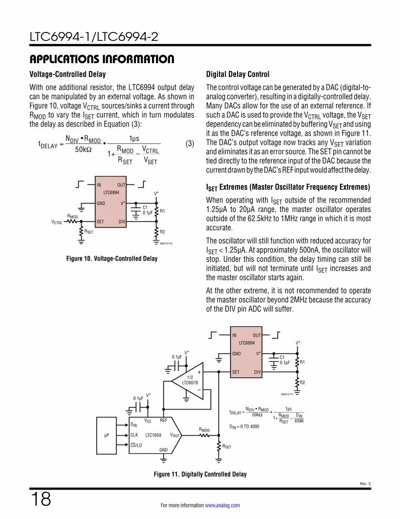
With one additional resistor, the LTC6994 output delay can be manipulated by an external voltage. As shown in Figure 10, voltage VCTRL sources/sinks a current through RMOD to vary the ISET current, which in turn modulates the delay as described in Equation (3):
tDELAY =NDIV •RMOD
50kΩ•
1µs
1+RMODRSET
–VCTRLVSET
(3)
Digital Delay Control
The control voltage can be generated by a DAC (digital-to-analog converter), resulting in a digitally-controlled delay. Many DACs allow for the use of an external reference. If such a DAC is used to provide the VCTRL voltage, the VSET dependency can be eliminated by buffering VSET and using it as the DAC’s reference voltage, as shown in Figure 11. The DAC’s output voltage now tracks any VSET variation and eliminates it as an error source. The SET pin cannot be tied directly to the reference input of the DAC because the current drawn by the DAC’s REF input would affect the delay.
ISET Extremes (Master Oscillator Frequency Extremes)
When operating with ISET outside of the recommended 1.25µA to 20µA range, the master oscillator operates outside of the 62.5kHz to 1MHz range in which it is most accurate.
The oscillator will still function with reduced accuracy for ISET < 1.25µA. At approximately 500nA, the oscillator will stop. Under this condition, the delay timing can still be initiated, but will not terminate until ISET increases and the master oscillator starts again.
At the other extreme, it is not recommended to operate the master oscillator beyond 2MHz because the accuracy of the DIV pin ADC will suffer.
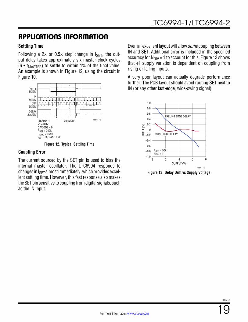
Following a 2× or 0.5× step change in ISET , the out-put delay takes approximately six master clock cycles (6 • tMASTER) to settle to within 1% of the final value. An example is shown in Figure 12, using the circuit in Figure 10.
The current sourced by the SET pin is used to bias the internal master oscillator. The LTC6994 responds to changes in ISET almost immediately, which provides excel-lent settling time. However, this fast response also makes the SET pin sensitive to coupling from digital signals, such as the IN input.
Even an excellent layout will allow some coupling between IN and SET. Additional error is included in the specified accuracy for NDIV = 1 to account for this. Figure 13 shows that ÷1 supply variation is dependent on coupling from rising or falling inputs.
A very poor layout can actually degrade performance further. The PCB layout should avoid routing SET next to IN (or any other fast-edge, wide-swing signal).
The Electrical Characteristics table specifies the supply current while the part is idle (waiting for an input transi-tion). IS(IDLE) varies with the programmed tDELAY and the supply voltage, as described by the equations in Table 2, valid for both the LTC6994-1 and LTC6994-2.
Table 2. Approximate Idle Supply Current EquationsCONDITION TYPICAL IS(IDLE)
NDIV ≤ 64
V + • NDIV • 7pF + 4pF( )tDELAY
+V +
500kΩ+ 2.2 •ISET + 50µA
NDIV ≥ 512
V + •NDIV • 7pF
tDELAY+
V +
500kΩ+ 1.8 •ISET + 50µA
When an input transition starts the delay timing circuity, the instantaneous supply current increases to IS(ACTIVE).
IS(ACTIVE) = IS(IDLE) + ∆IS(ACTIVE)
APPLICATIONS INFORMATION∆IS(ACTIVE) can be estimated using the equations in Table 3, assuming a periodic input with frequency fIN. The equa-tions assume the input pulse width is greater than tDELAY; otherwise, the output will not transition (and the increase in supply current will be less).
Table 3. Active Increase in Supply CurrentCONDITION DEVICE TYPICAL ∆IS(ACTIVE)*
Figures 14 and 15 show how the supply current increases from IS(IDLE) as the input frequency increases. At higher NDIV settings, the increase in active current is smaller.
fIN • tDELAY
“IDLE”
POW
ER S
UPPL
Y CU
RREN
T (µ
A)
150
200
250
0.8
699412 F14
100
50
00.2 0.4 0.6 1.0
÷1, RSET = 50k÷8, RSET = 50k
÷1, RSET = 100k
÷1, RSET = 800k
V+ = 3.3VINPUT PULSE WIDTH = 1.1 • tDELAY
CLOAD = 5pFRLOAD = ∞
fIN • tDELAY
“IDLE”
POW
ER S
UPPL
Y CU
RREN
T (µ
A)
150
200
250
0.4
699412 F15
100
50
00.1 0.2 0.3 0.5
÷1, RSET = 50k÷8, RSET = 50k
÷1, RSET = 100k
÷1, RSET = 800k
V+ = 3.3VfIN < 1/(2 • tDELAY) TO ALLOW RISING AND FALLING DELAYS TO REACH THE OUTPUT
CLOAD = 5pFRLOAD = ∞
Figure 14. IS(ACTIVE) vs Input Frequency, LTC6994-1 Figure 15. IS(ACTIVE) vs Input Frequency, LTC6994-2
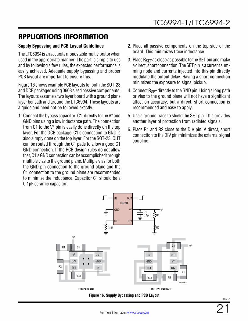
The LTC6994 is an accurate monostable multivibrator when used in the appropriate manner. The part is simple to use and by following a few rules, the expected performance is easily achieved. Adequate supply bypassing and proper PCB layout are important to ensure this.
Figure 16 shows example PCB layouts for both the SOT-23 and DCB packages using 0603 sized passive components. The layouts assume a two layer board with a ground plane layer beneath and around the LTC6994. These layouts are a guide and need not be followed exactly.
1. Connect the bypass capacitor, C1, directly to the V+ and GND pins using a low inductance path. The connection from C1 to the V+ pin is easily done directly on the top layer. For the DCB package, C1’s connection to GND is also simply done on the top layer. For the SOT-23, OUT can be routed through the C1 pads to allow a good C1 GND connection. If the PCB design rules do not allow that, C1’s GND connection can be accomplished through multiple vias to the ground plane. Multiple vias for both the GND pin connection to the ground plane and the C1 connection to the ground plane are recommended to minimize the inductance. Capacitor C1 should be a 0.1µF ceramic capacitor.
2. Place all passive components on the top side of the board. This minimizes trace inductance.
3. Place RSET as close as possible to the SET pin and make a direct, short connection. The SET pin is a current sum-ming node and currents injected into this pin directly modulate the output delay. Having a short connection minimizes the exposure to signal pickup.
4. Connect RSET directly to the GND pin. Using a long path or vias to the ground plane will not have a significant affect on accuracy, but a direct, short connection is recommended and easy to apply.
5. Use a ground trace to shield the SET pin. This provides another layer of protection from radiated signals.
6. Place R1 and R2 close to the DIV pin. A direct, short connection to the DIV pin minimizes the external signal coupling.
NOTE:1. DRAWING TO BE MADE A JEDEC PACKAGE OUTLINE M0-229 VARIATION OF (TBD)2. DRAWING NOT TO SCALE3. ALL DIMENSIONS ARE IN MILLIMETERS4. DIMENSIONS OF EXPOSED PAD ON BOTTOM OF PACKAGE DO NOT INCLUDE MOLD FLASH. MOLD FLASH, IF PRESENT, SHALL NOT EXCEED 0.15mm ON ANY SIDE5. EXPOSED PAD SHALL BE SOLDER PLATED 6. SHADED AREA IS ONLY A REFERENCE FOR PIN 1 LOCATION ON THE TOP AND BOTTOM OF PACKAGE
NOTE:1. DIMENSIONS ARE IN MILLIMETERS2. DRAWING NOT TO SCALE3. DIMENSIONS ARE INCLUSIVE OF PLATING4. DIMENSIONS ARE EXCLUSIVE OF MOLD FLASH AND METAL BURR5. MOLD FLASH SHALL NOT EXCEED 0.254mm6. JEDEC PACKAGE REFERENCE IS MO-193
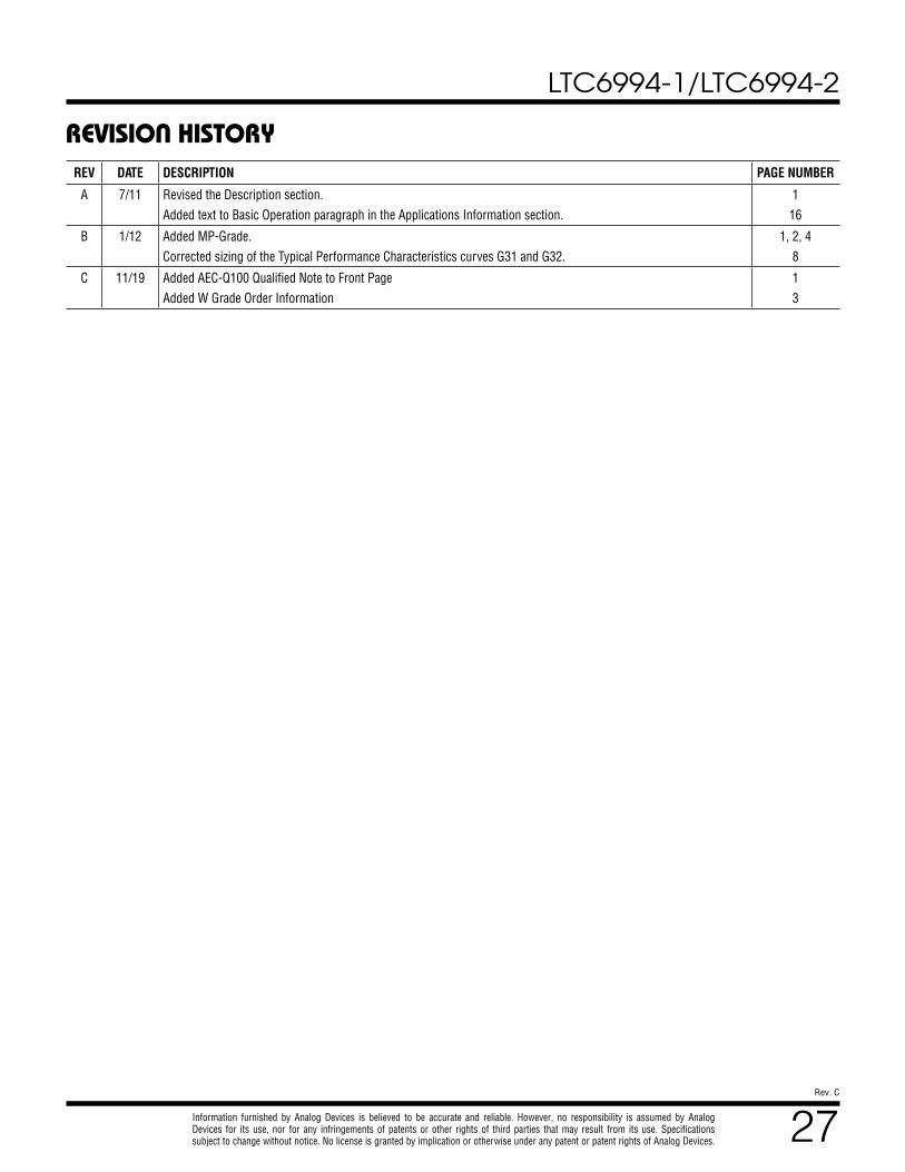
A 7/11 Revised the Description section.Added text to Basic Operation paragraph in the Applications Information section.
116
B 1/12 Added MP-Grade.Corrected sizing of the Typical Performance Characteristics curves G31 and G32.
1, 2, 48
C 11/19 Added AEC-Q100 Qualified Note to Front PageAdded W Grade Order Information
13
Information furnished by Analog Devices is believed to be accurate and reliable. However, no responsibility is assumed by Analog Devices for its use, nor for any infringements of patents or other rights of third parties that may result from its use. Specifications subject to change without notice. No license is granted by implication or otherwise under any patent or patent rights of Analog Devices.