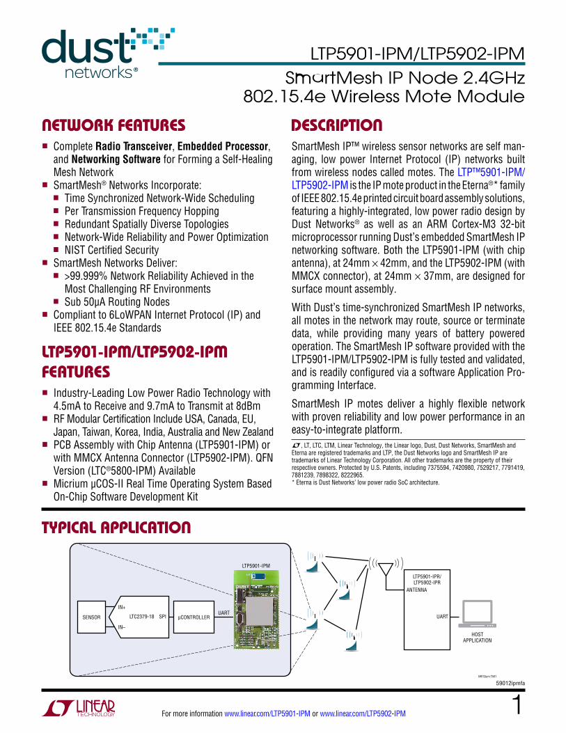
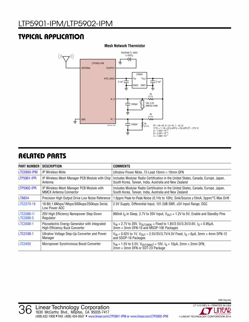
LTP5901-IPM/LTP5902-IPM 1 59012ipmfa For more information www.linear.com/LTP5901-IPM or www.linear.com/LTP5902-IPM TYPICAL APPLICATION NETWORK FEATURES DESCRIPTION SmartMesh IP Node 2.4GHz 802.15.4e Wireless Mote Module SmartMesh IP™ wireless sensor networks are self man- aging, low power Internet Protocol (IP) networks built from wireless nodes called motes. The LTP™5901-IPM/ LTP5902-IPM is the IP mote product in the Eterna ® * family of IEEE 802.15.4e printed circuit board assembly solutions, featuring a highly-integrated, low power radio design by Dust Networks ® as well as an ARM Cortex-M3 32-bit microprocessor running Dust’s embedded SmartMesh IP networking software. Both the LTP5901-IPM (with chip antenna), at 24mm × 42mm, and the LTP5902-IPM (with MMCX connector), at 24mm × 37mm, are designed for surface mount assembly. With Dust’s time-synchronized SmartMesh IP networks, all motes in the network may route, source or terminate data, while providing many years of battery powered operation. The SmartMesh IP software provided with the LTP5901-IPM/LTP5902-IPM is fully tested and validated, and is readily configured via a software Application Pro- gramming Interface. SmartMesh IP motes deliver a highly flexible network with proven reliability and low power performance in an easy-to-integrate platform. LTP5901-IPM/LTP5902-IPM FEATURES n Complete Radio Transceiver, Embedded Processor, and Networking Software for Forming a Self-Healing Mesh Network n SmartMesh ® Networks Incorporate: n Time Synchronized Network-Wide Scheduling n Per Transmission Frequency Hopping n Redundant Spatially Diverse Topologies n Network-Wide Reliability and Power Optimization n NIST Certified Security n SmartMesh Networks Deliver: n >99.999% Network Reliability Achieved in the Most Challenging RF Environments n Sub 50µA Routing Nodes n Compliant to 6LoWPAN Internet Protocol (IP) and IEEE 802.15.4e Standards n Industry-Leading Low Power Radio Technology with 4.5mA to Receive and 9.7mA to Transmit at 8dBm n RF Modular Certification Include USA, Canada, EU, Japan, Taiwan, Korea, India, Australia and New Zealand n PCB Assembly with Chip Antenna (LTP5901-IPM) or with MMCX Antenna Connector (LTP5902-IPM). QFN Version (LTC ® 5800-IPM) Available n Micrium µCOS-II Real Time Operating System Based On-Chip Software Development Kit L, LT, LTC, LTM, Linear Technology, the Linear logo, Dust, Dust Networks, SmartMesh and Eterna are registered trademarks and LTP, the Dust Networks logo and SmartMesh IP are trademarks of Linear Technology Corporation. All other trademarks are the property of their respective owners. Protected by U.S. Patents, including 7375594, 7420980, 7529217, 7791419, 7881239, 7898322, 8222965. * Eterna is Dust Networks’ low power radio SoC architecture. 59012ipm TA01 μCONTROLLER SENSOR IN+ IN– SPI LTC2379-18 LTP5901-IPR/ LTP5902-IPR UART ANTENNA HOST APPLICATION UART LTP5901-IPM
Transcript
LTP5901-IPM/LTP5902-IPM
159012ipmfa
For more information www.linear.com/LTP5901-IPM or www.linear.com/LTP5902-IPM
Typical applicaTion
neTwork FeaTures DescripTion
SmartMesh IP Node 2.4GHz 802.15.4e Wireless Mote Module
SmartMesh IP™ wireless sensor networks are self man-aging, low power Internet Protocol (IP) networks built from wireless nodes called motes. The LTP™5901-IPM/LTP5902-IPM is the IP mote product in the Eterna®* family of IEEE 802.15.4e printed circuit board assembly solutions, featuring a highly-integrated, low power radio design by Dust Networks® as well as an ARM Cortex-M3 32-bit microprocessor running Dust’s embedded SmartMesh IP networking software. Both the LTP5901-IPM (with chip antenna), at 24mm × 42mm, and the LTP5902-IPM (with MMCX connector), at 24mm × 37mm, are designed for surface mount assembly.
With Dust’s time-synchronized SmartMesh IP networks, all motes in the network may route, source or terminate data, while providing many years of battery powered operation. The SmartMesh IP software provided with the LTP5901-IPM/LTP5902-IPM is fully tested and validated, and is readily configured via a software Application Pro-gramming Interface.
SmartMesh IP motes deliver a highly flexible network with proven reliability and low power performance in an easy-to-integrate platform.
lTp5901-ipM/lTp5902-ipM FeaTures
n Complete Radio Transceiver, Embedded Processor, and Networking Software for Forming a Self-Healing Mesh Network
n SmartMesh® Networks Incorporate:n Time Synchronized Network-Wide Schedulingn Per Transmission Frequency Hoppingn Redundant Spatially Diverse Topologiesn Network-Wide Reliability and Power Optimizationn NIST Certified Security
n SmartMesh Networks Deliver:n >99.999% Network Reliability Achieved in the
Most Challenging RF Environmentsn Sub 50µA Routing Nodes
n Compliant to 6LoWPAN Internet Protocol (IP) and IEEE 802.15.4e Standards
n Industry-Leading Low Power Radio Technology with 4.5mA to Receive and 9.7mA to Transmit at 8dBm
n RF Modular Certification Include USA, Canada, EU, Japan, Taiwan, Korea, India, Australia and New Zealand
n PCB Assembly with Chip Antenna (LTP5901-IPM) or with MMCX Antenna Connector (LTP5902-IPM). QFN Version (LTC®5800-IPM) Available
n Micrium µCOS-II Real Time Operating System Based On-Chip Software Development Kit
L, LT, LTC, LTM, Linear Technology, the Linear logo, Dust, Dust Networks, SmartMesh and Eterna are registered trademarks and LTP, the Dust Networks logo and SmartMesh IP are trademarks of Linear Technology Corporation. All other trademarks are the property of their respective owners. Protected by U.S. Patents, including 7375594, 7420980, 7529217, 7791419, 7881239, 7898322, 8222965. * Eterna is Dust Networks’ low power radio SoC architecture.
For more information www.linear.com/LTP5901-IPM or www.linear.com/LTP5902-IPM
Table oF conTenTs Network Features .......................................... 1LTP5901-IPM/LTP5902-IPM Features ................... 1Typical Application ........................................ 1Description.................................................. 1Table of Contents .......................................... 2SmartMesh Network Overview ........................... 3Absolute Maximum Ratings .............................. 4Pin Configuration .......................................... 4Order Information .......................................... 5Recommended Operating Conditions ................... 5DC Characteristics ......................................... 5Radio Specifications ...................................... 6Radio Receiver Characteristics .......................... 6Radio Transmitter Characteristics ....................... 7Digital I/O Characteristics ................................ 7Temperature Sensor Characteristics .................... 8Analog Input Chain Characteristics ..................... 8System Characteristics ................................... 8UART AC Characteristics .................................. 9TIMEn AC Characteristics ................................ 10Radio_Inhibit AC Characteristics ....................... 10Flash AC Characteristics ................................. 11Flash SPI Slave AC Characteristics .................... 11SPI Master AC Characteristics .......................... 12I2C AC Characteristics .................................... 131-Wire Master ............................................. 13Flash SPI Slave AC Characteristics .................... 14Typical Performance Characteristics .................. 15Pin Functions .............................................. 20
Operation................................................... 24Power Supply .......................................................... 24Supply Monitoring and Reset .................................25Precision Timing .....................................................25Application Time Synchronization ..........................25Time References .....................................................25Radio ......................................................................26UARTs .....................................................................26Autonomous MAC ...................................................27Security ..................................................................27Temperature Sensor ...............................................27RADIO INHIBIT .......................................................27Software Installation ...............................................27Flash Data Retention ...............................................28State Diagram .........................................................28I2C Master ..............................................................30SPI Master ..............................................................301-Wire Master .........................................................30
Applications Information ................................ 31Modes of Operation ................................................ 31Regulatory and Standards Compliance ................... 31Soldering Information .............................................32
Related Documentation .................................. 32Package Description ..................................... 33Revision History .......................................... 35Typical Application ....................................... 36Related Parts .............................................. 36
For more information www.linear.com/LTP5901-IPM or www.linear.com/LTP5902-IPM
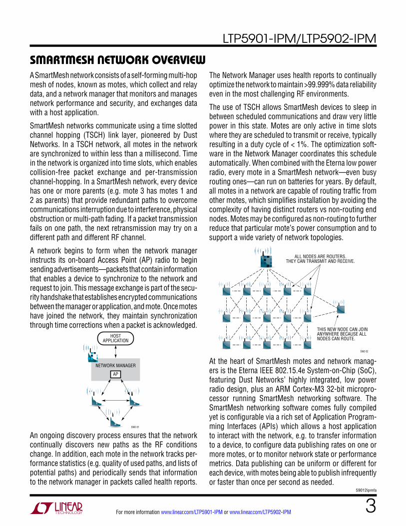
sMarTMesh neTwork overviewThe Network Manager uses health reports to continually optimize the network to maintain >99.999% data reliability even in the most challenging RF environments.
The use of TSCH allows SmartMesh devices to sleep in between scheduled communications and draw very little power in this state. Motes are only active in time slots where they are scheduled to transmit or receive, typically resulting in a duty cycle of < 1%. The optimization soft-ware in the Network Manager coordinates this schedule automatically. When combined with the Eterna low power radio, every mote in a SmartMesh network—even busy routing ones—can run on batteries for years. By default, all motes in a network are capable of routing traffic from other motes, which simplifies installation by avoiding the complexity of having distinct routers vs non-routing end nodes. Motes may be configured as non-routing to further reduce that particular mote’s power consumption and to support a wide variety of network topologies.
A SmartMesh network consists of a self-forming multi-hop mesh of nodes, known as motes, which collect and relay data, and a network manager that monitors and manages network performance and security, and exchanges data with a host application.
SmartMesh networks communicate using a time slotted channel hopping (TSCH) link layer, pioneered by Dust Networks. In a TSCH network, all motes in the network are synchronized to within less than a millisecond. Time in the network is organized into time slots, which enables collision-free packet exchange and per-transmission channel-hopping. In a SmartMesh network, every device has one or more parents (e.g. mote 3 has motes 1 and 2 as parents) that provide redundant paths to overcome communications interruption due to interference, physical obstruction or multi-path fading. If a packet transmission fails on one path, the next retransmission may try on a different path and different RF channel.
A network begins to form when the network manager instructs its on-board Access Point (AP) radio to begin sending advertisements—packets that contain information that enables a device to synchronize to the network and request to join. This message exchange is part of the secu-rity handshake that establishes encrypted communications between the manager or application, and mote. Once motes have joined the network, they maintain synchronization through time corrections when a packet is acknowledged.
At the heart of SmartMesh motes and network manag-ers is the Eterna IEEE 802.15.4e System-on-Chip (SoC), featuring Dust Networks’ highly integrated, low power radio design, plus an ARM Cortex-M3 32-bit micropro-cessor running SmartMesh networking software. The SmartMesh networking software comes fully compiled yet is configurable via a rich set of Application Program-ming Interfaces (APIs) which allows a host application to interact with the network, e.g. to transfer information to a device, to configure data publishing rates on one or more motes, or to monitor network state or performance metrics. Data publishing can be uniform or different for each device, with motes being able to publish infrequently or faster than once per second as needed.
An ongoing discovery process ensures that the network continually discovers new paths as the RF conditions change. In addition, each mote in the network tracks per-formance statistics (e.g. quality of used paths, and lists of potential paths) and periodically sends that information to the network manager in packets called health reports.
ALL NODES ARE ROUTERS.THEY CAN TRANSMIT AND RECEIVE.
THIS NEW NODE CAN JOINANYWHERE BECAUSE ALLNODES CAN ROUTE.
For more information www.linear.com/LTP5901-IPM or www.linear.com/LTP5902-IPM
absoluTe MaxiMuM raTings
Supply Voltage on VSUPPLY ..................................4.20VInput Voltage on AI_0/1/2/3 Inputs ........................1.98VVoltage on Any Digital I/O pin .................................... –0.3V to VSUPPLY + 0.3VInput RF Level .................................................... +10dBmStorage Temperature Range (Note 3) ..... –55°C to 105°COperating Temperature Range
LTP5901I/LPT5902I .............................–40°C to 85°C
CAUTION: This part is sensitive to electrostatic discharge (ESD). It is very important that proper ESD precautions be observed when handling the LTP5901-IPM/LTP5902-IPM.
Pin functions shown in italics are currently not supported in software.pin conFiguraTion
For more information www.linear.com/LTP5901-IPM or www.linear.com/LTP5902-IPM
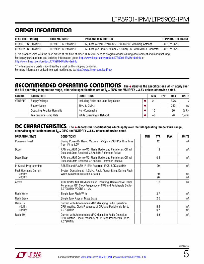
orDer inForMaTionLEAD FREE FINISH† PART MARKING* PACKAGE DESCRIPTION TEMPERATURE RANGE
LTP5901IPC-IPMA#PBF LTP5901IPC-IPMA#PBF 66-Lead (42mm × 24mm × 5.5mm) PCB with Chip Antenna –40°C to 85°C
LTP5902IPC-IPMA#PBF LTP5902IPC-IPMA#PBF 66-Lead (37.5mm × 24mm × 5.5mm) PCB with MMCX Connector –40°C to 85°C
†This product ships with the flash erased at the time of order. OEMs will need to program devices during development and manufacturing. For legacy part numbers and ordering information go to: http://www.linear.com/product/LTP5901-IPM#orderinfo or http://www.linear.com/product/LTP5902-IPM#orderinfo
*The temperature grade is identified by a label on the shipping container. For more information on lead free part marking, go to: http://www.linear.com/leadfree/
recoMMenDeD operaTing conDiTions The l denotes the specifications which apply over the full operating temperature range, otherwise specifications are at TA = 25°C and VSUPPLY = 3.6V unless otherwise noted.
SYMBOL PARAMETER CONDITIONS MIN TYP MAX UNITS
VSUPPLY Supply Voltage Including Noise and Load Regulation l 2.1 3.76 V
Supply Noise 50Hz to 2MHz l 250 mV
Operating Relative Humidity Non-Condensing l 10 90 % RH
Temperature Ramp Rate While Operating in Network l –8 +8 °C/min
Dc characTerisTics The l denotes the specifications which apply over the full operating temperature range, otherwise specifications are at TA = 25°C and VSUPPLY = 3.6V unless otherwise noted.
OPERATION/STATE CONDITIONS MIN TYP MAX UNITS
Power-on Reset During Power-On Reset, Maximum 750µs + VSUPPLY Rise Time from 1V to 1.9V
12 mA
Doze RAM on, ARM Cortex-M3, Flash, Radio, and Peripherals Off, All Data and State Retained, 32.768kHz Reference Active
1.2 µA
Deep Sleep RAM on, ARM Cortex-M3, Flash, Radio, and Peripherals Off, All Data and State Retained, 32.768kHz Reference Inactive
0.8 µA
In-Circuit Programming RESETn and FLASH_P_ENn Asserted, IPCS_SCK at 8MHz 20 mA
Peak Operating Current +8dBm +0dBm
System Operating at 14.7MHz, Radio Transmitting, During Flash Write. Maximum Duration 4.33 ms.
30 26
mA mA
Active ARM Cortex M3, RAM and Flash Operating, Radio and All Other Peripherals Off. Clock Frequency of CPU and Peripherals Set to 7.3728MHz, VCORE = 1.2V
1.3 mA
Flash Write Single Bank Flash Write 3.7 mA
Flash Erase Single Bank Page or Mass Erase 2.5 mA
Radio Tx +0dBm +8dBm
Current with Autonomous MAC Managing Radio Operation, CPU Inactive. Clock Frequency of CPU and Peripherals Set to 7.3728MHz.
5.4 9.7
mA mA
Radio Rx Current with Autonomous MAC Managing Radio Operation, CPU Inactive. Clock Frequency of CPU and Peripherals Set to 7.3728MHz.
For more information www.linear.com/LTP5901-IPM or www.linear.com/LTP5902-IPM
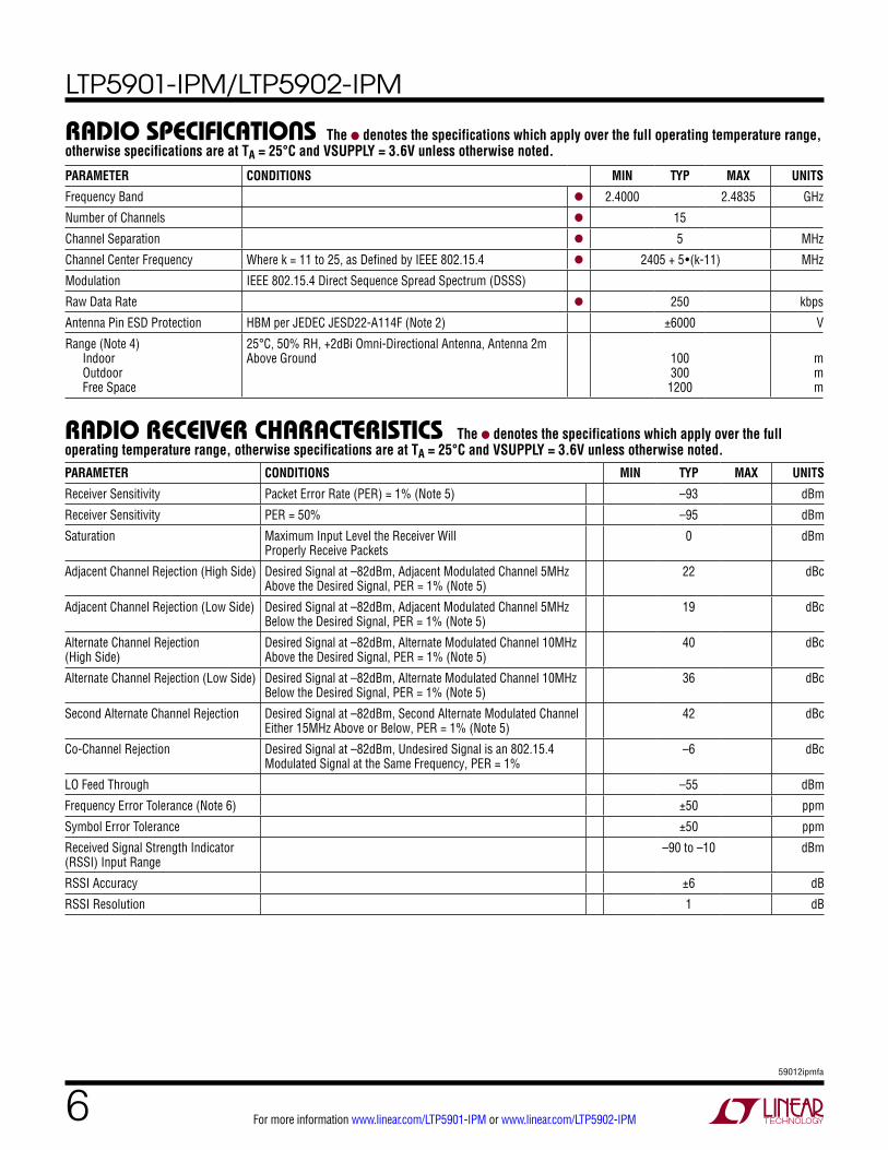
raDio receiver characTerisTics The l denotes the specifications which apply over the full operating temperature range, otherwise specifications are at TA = 25°C and VSUPPLY = 3.6V unless otherwise noted.
Saturation Maximum Input Level the Receiver Will Properly Receive Packets
0 dBm
Adjacent Channel Rejection (High Side) Desired Signal at –82dBm, Adjacent Modulated Channel 5MHz Above the Desired Signal, PER = 1% (Note 5)
22 dBc
Adjacent Channel Rejection (Low Side) Desired Signal at –82dBm, Adjacent Modulated Channel 5MHz Below the Desired Signal, PER = 1% (Note 5)
19 dBc
Alternate Channel Rejection (High Side)
Desired Signal at –82dBm, Alternate Modulated Channel 10MHz Above the Desired Signal, PER = 1% (Note 5)
40 dBc
Alternate Channel Rejection (Low Side) Desired Signal at –82dBm, Alternate Modulated Channel 10MHz Below the Desired Signal, PER = 1% (Note 5)
36 dBc
Second Alternate Channel Rejection Desired Signal at –82dBm, Second Alternate Modulated Channel Either 15MHz Above or Below, PER = 1% (Note 5)
42 dBc
Co-Channel Rejection Desired Signal at –82dBm, Undesired Signal is an 802.15.4 Modulated Signal at the Same Frequency, PER = 1%
–6 dBc
LO Feed Through –55 dBm
Frequency Error Tolerance (Note 6) ±50 ppm
Symbol Error Tolerance ±50 ppm
Received Signal Strength Indicator (RSSI) Input Range
–90 to –10 dBm
RSSI Accuracy ±6 dB
RSSI Resolution 1 dB
raDio speciFicaTions The l denotes the specifications which apply over the full operating temperature range, otherwise specifications are at TA = 25°C and VSUPPLY = 3.6V unless otherwise noted.
PARAMETER CONDITIONS MIN TYP MAX UNITS
Frequency Band l 2.4000 2.4835 GHz
Number of Channels l 15
Channel Separation l 5 MHz
Channel Center Frequency Where k = 11 to 25, as Defined by IEEE 802.15.4 l 2405 + 5•(k-11) MHz
Modulation IEEE 802.15.4 Direct Sequence Spread Spectrum (DSSS)
Raw Data Rate l 250 kbps
Antenna Pin ESD Protection HBM per JEDEC JESD22-A114F (Note 2) ±6000 V
For more information www.linear.com/LTP5901-IPM or www.linear.com/LTP5902-IPM
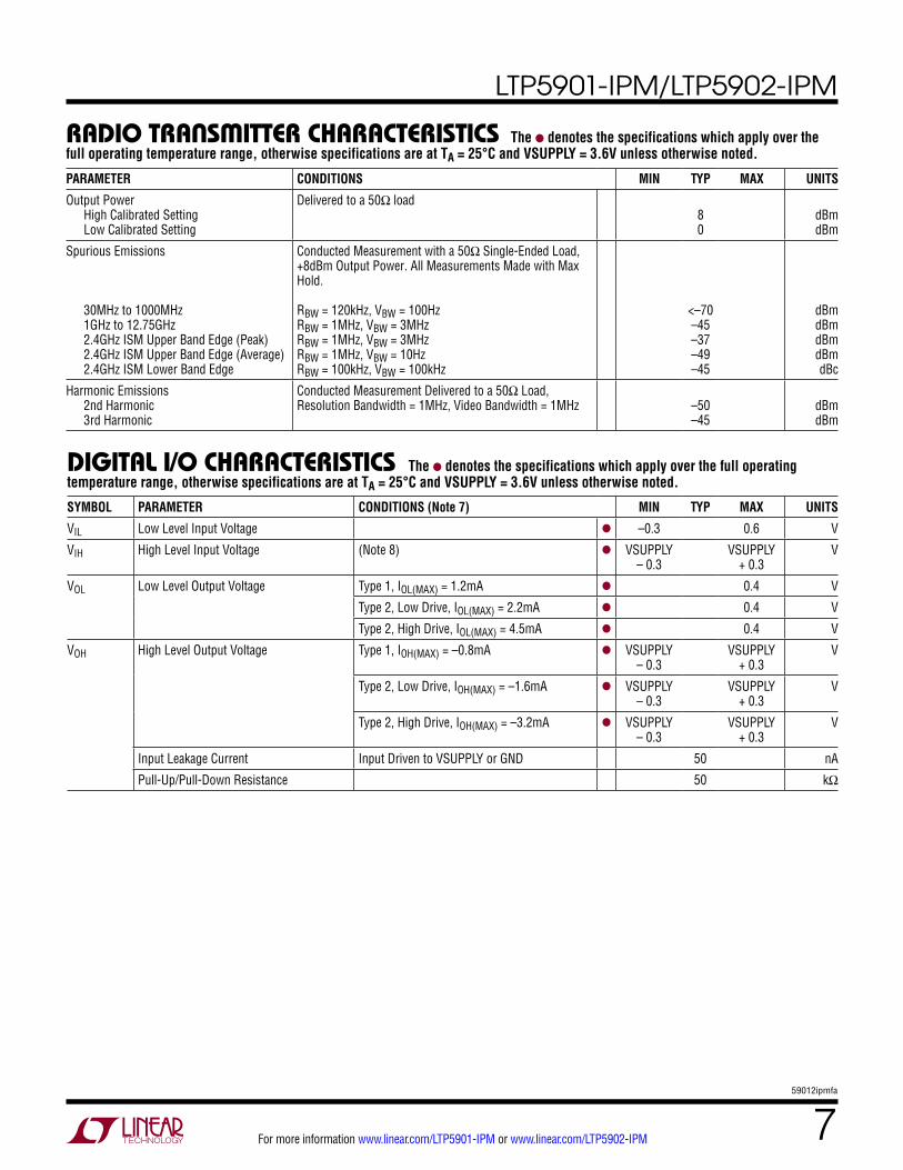
raDio TransMiTTer characTerisTics The l denotes the specifications which apply over the full operating temperature range, otherwise specifications are at TA = 25°C and VSUPPLY = 3.6V unless otherwise noted.
PARAMETER CONDITIONS MIN TYP MAX UNITS
Output Power High Calibrated Setting Low Calibrated Setting
Delivered to a 50Ω load 8 0
dBm dBm
Spurious Emissions 30MHz to 1000MHz 1GHz to 12.75GHz 2.4GHz ISM Upper Band Edge (Peak) 2.4GHz ISM Upper Band Edge (Average) 2.4GHz ISM Lower Band Edge
Conducted Measurement with a 50Ω Single-Ended Load, +8dBm Output Power. All Measurements Made with Max Hold. RBW = 120kHz, VBW = 100Hz RBW = 1MHz, VBW = 3MHz RBW = 1MHz, VBW = 3MHz RBW = 1MHz, VBW = 10Hz RBW = 100kHz, VBW = 100kHz
<–70 –45 –37 –49 –45
dBm dBm dBm dBm dBc
Harmonic Emissions 2nd Harmonic 3rd Harmonic
Conducted Measurement Delivered to a 50Ω Load, Resolution Bandwidth = 1MHz, Video Bandwidth = 1MHz
–50 –45
dBm dBm
DigiTal i/o characTerisTics The l denotes the specifications which apply over the full operating temperature range, otherwise specifications are at TA = 25°C and VSUPPLY = 3.6V unless otherwise noted.
SYMBOL PARAMETER CONDITIONS (Note 7) MIN TYP MAX UNITS
VIL Low Level Input Voltage l –0.3 0.6 V
VIH High Level Input Voltage (Note 8) l VSUPPLY – 0.3
VSUPPLY + 0.3
V
VOL Low Level Output Voltage Type 1, IOL(MAX) = 1.2mA l 0.4 V
Type 2, Low Drive, IOL(MAX) = 2.2mA l 0.4 V
Type 2, High Drive, IOL(MAX) = 4.5mA l 0.4 V
VOH High Level Output Voltage Type 1, IOH(MAX) = –0.8mA l VSUPPLY – 0.3
VSUPPLY + 0.3
V
Type 2, Low Drive, IOH(MAX) = –1.6mA l VSUPPLY – 0.3
VSUPPLY + 0.3
V
Type 2, High Drive, IOH(MAX) = –3.2mA l VSUPPLY – 0.3
VSUPPLY + 0.3
V
Input Leakage Current Input Driven to VSUPPLY or GND 50 nA
For more information www.linear.com/LTP5901-IPM or www.linear.com/LTP5902-IPM
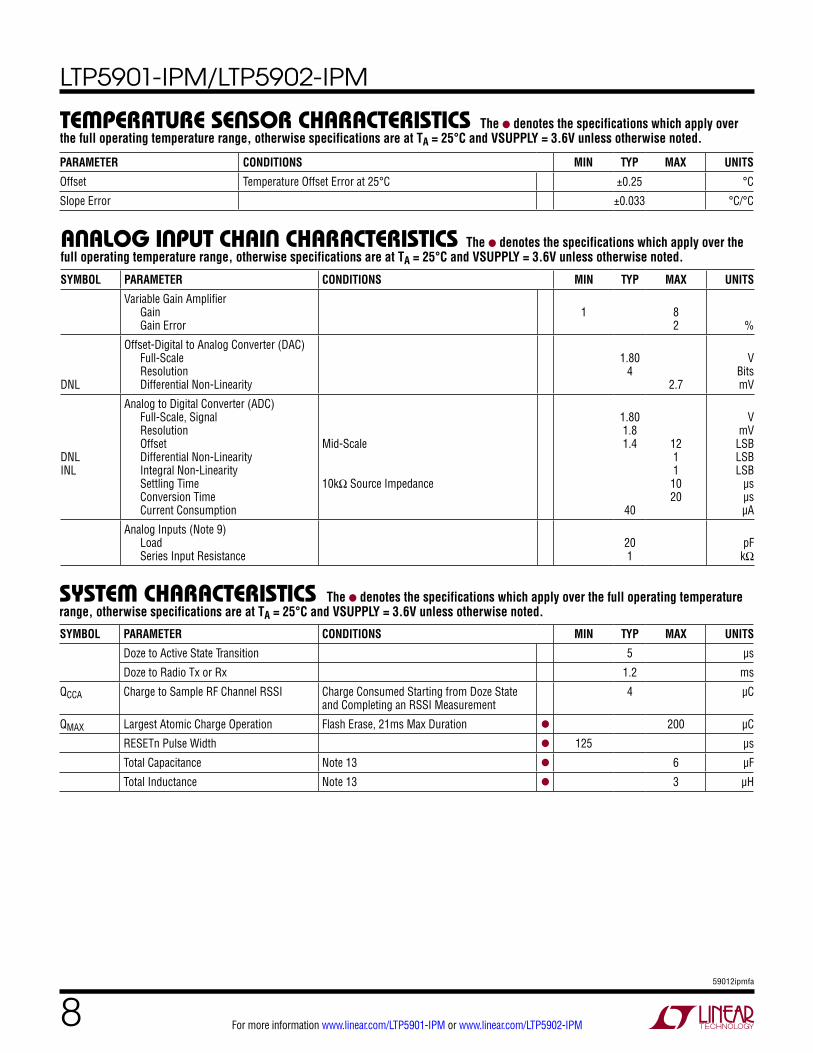
TeMperaTure sensor characTerisTics The l denotes the specifications which apply over the full operating temperature range, otherwise specifications are at TA = 25°C and VSUPPLY = 3.6V unless otherwise noted.
PARAMETER CONDITIONS MIN TYP MAX UNITS
Offset Temperature Offset Error at 25°C ±0.25 °C
Slope Error ±0.033 °C/°C
analog inpuT chain characTerisTics The l denotes the specifications which apply over the full operating temperature range, otherwise specifications are at TA = 25°C and VSUPPLY = 3.6V unless otherwise noted.
SYMBOL PARAMETER CONDITIONS MIN TYP MAX UNITS
Variable Gain Amplifier Gain Gain Error
1
8 2
%
DNL
Offset-Digital to Analog Converter (DAC) Full-Scale Resolution Differential Non-Linearity
1.80
4
2.7
V
Bits mV
DNL INL
Analog to Digital Converter (ADC) Full-Scale, Signal Resolution Offset Differential Non-Linearity Integral Non-Linearity Settling Time Conversion Time Current Consumption
Mid-Scale 10kΩ Source Impedance
1.80 1.8 1.4
40
12 1 1
10 20
V
mV LSB LSB LSB
µs µs µA
Analog Inputs (Note 9) Load Series Input Resistance
20 1
pF
kΩ
sysTeM characTerisTics The l denotes the specifications which apply over the full operating temperature range, otherwise specifications are at TA = 25°C and VSUPPLY = 3.6V unless otherwise noted.
SYMBOL PARAMETER CONDITIONS MIN TYP MAX UNITS
Doze to Active State Transition 5 µs
Doze to Radio Tx or Rx 1.2 ms
QCCA Charge to Sample RF Channel RSSI Charge Consumed Starting from Doze State and Completing an RSSI Measurement
4 µC
QMAX Largest Atomic Charge Operation Flash Erase, 21ms Max Duration l 200 µC
For more information www.linear.com/LTP5901-IPM or www.linear.com/LTP5902-IPM
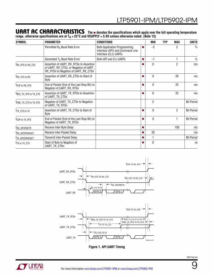
uarT ac characTerisTics The l denotes the specifications which apply over the full operating temperature range, otherwise specifications are at TA = 25°C and VSUPPLY = 3.6V unless otherwise noted. (Note 13)
SYMBOL PARAMETER CONDITIONS MIN TYP MAX UNITS
Permitted RX Baud Rate Error Both Application Programming Interface (API) and Command Line Interface (CLI) UARTs
l –2 2 %
Generated TX Baud Rate Error Both API and CLI UARTs l –1 1 %
tRX_RTS to RX_CTS Assertion of UART_RX_RTSn to Assertion of UART_RX_CTSn, or Negation of UART_RX_RTSn to Negation of UART_RX_CTSn
l 0 2 ms
tRX_CTS to RX Assertion of UART_RX_CTSn to Start of Byte
l 0 20 ms
tEOP to RX_RTS End of Packet (End of the Last Stop Bit) to Negation of UART_RX_RTSn
l 0 22 ms
tBEG_TX_RTS to TX_CTS Assertion of UART_TX_RTSn to Assertion of UART_TX_CTSn
l 0 22 ms
tEND_TX_CTS to TX_RTS Negation of UART_TX_CTSn to Negation of UART_TX_RTSn
2 Bit Period
tTX_CTS to TX Assertion of UART_TX_CTSn to Start of Byte
l 0 2 Bit Period
tEOP to TX_RTS End of Packet (End of the Last Stop Bit) to Negation of UART_TX_RTSn
l 0 1 Bit Period
tRX_INTERBYTE Receive Inter-Byte Delay l 100 ms
tRX_INTERPACKET Receive Inter-Packet Delay l 20 ms
tTX_INTERPACKET Transmit Inter-Packet Delay l 1 Bit Period
tTX to TX_CTS Start of Byte to Negation of UART_TX_CTSn
For more information www.linear.com/LTP5901-IPM or www.linear.com/LTP5902-IPM
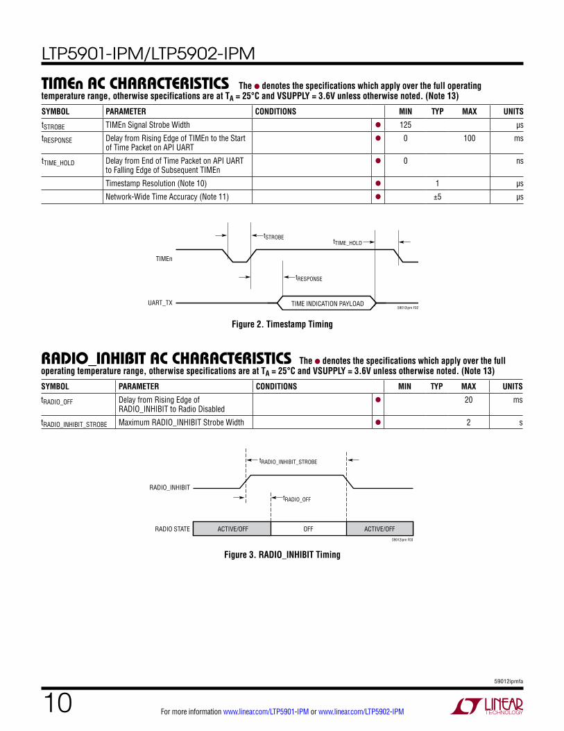
TiMen ac characTerisTics The l denotes the specifications which apply over the full operating temperature range, otherwise specifications are at TA = 25°C and VSUPPLY = 3.6V unless otherwise noted. (Note 13)
SYMBOL PARAMETER CONDITIONS MIN TYP MAX UNITS
tSTROBE TIMEn Signal Strobe Width l 125 µs
tRESPONSE Delay from Rising Edge of TIMEn to the Start of Time Packet on API UART
l 0 100 ms
tTIME_HOLD Delay from End of Time Packet on API UART to Falling Edge of Subsequent TIMEn
l 0 ns
Timestamp Resolution (Note 10) l 1 µs
Network-Wide Time Accuracy (Note 11) l ±5 µs
59012ipm F02
TIMEn
UART_TX
tSTROBEtTIME_HOLD
tRESPONSE
TIME INDICATION PAYLOAD
Figure 2. Timestamp Timing
raDio_inhibiT ac characTerisTics The l denotes the specifications which apply over the full operating temperature range, otherwise specifications are at TA = 25°C and VSUPPLY = 3.6V unless otherwise noted. (Note 13)
SYMBOL PARAMETER CONDITIONS MIN TYP MAX UNITS
tRADIO_OFF Delay from Rising Edge of RADIO_INHIBIT to Radio Disabled
l 20 ms
tRADIO_INHIBIT_STROBE Maximum RADIO_INHIBIT Strobe Width l 2 s
For more information www.linear.com/LTP5901-IPM or www.linear.com/LTP5902-IPM
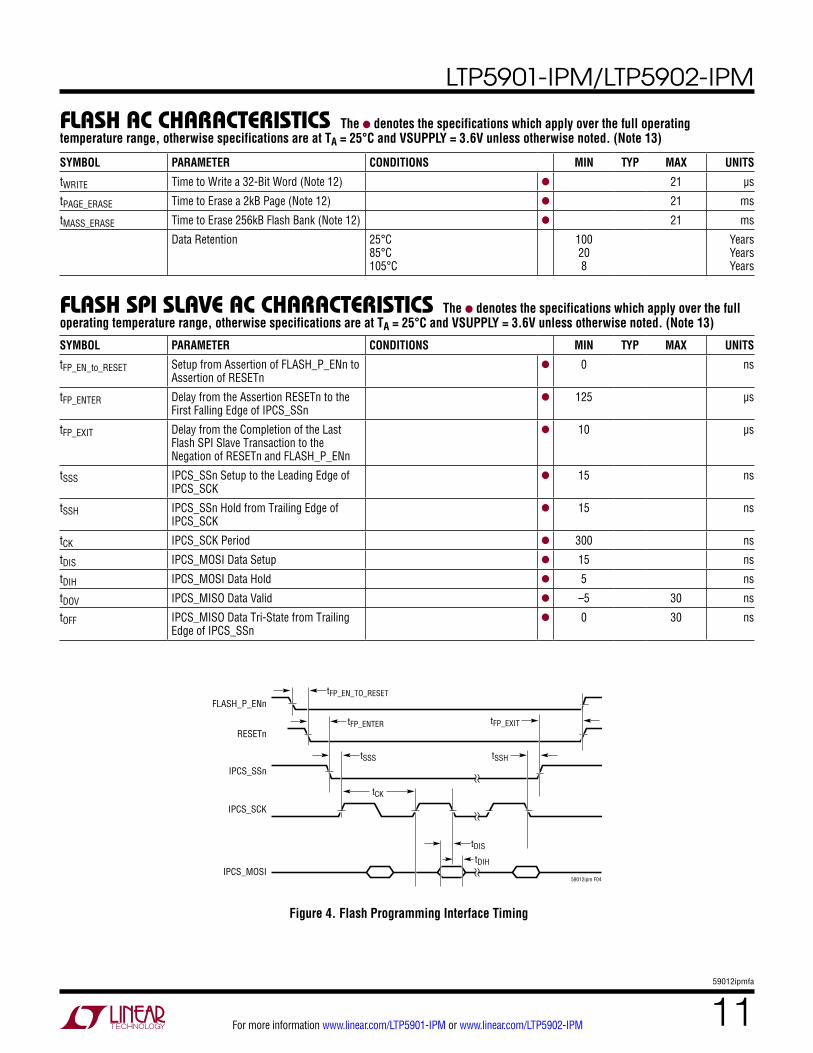
Flash ac characTerisTics The l denotes the specifications which apply over the full operating temperature range, otherwise specifications are at TA = 25°C and VSUPPLY = 3.6V unless otherwise noted. (Note 13)
SYMBOL PARAMETER CONDITIONS MIN TYP MAX UNITS
tWRITE Time to Write a 32-Bit Word (Note 12) l 21 µs
tPAGE_ERASE Time to Erase a 2kB Page (Note 12) l 21 ms
tMASS_ERASE Time to Erase 256kB Flash Bank (Note 12) l 21 ms
Data Retention 25°C 85°C 105°C
100 20 8
Years Years Years
Flash spi slave ac characTerisTics The l denotes the specifications which apply over the full operating temperature range, otherwise specifications are at TA = 25°C and VSUPPLY = 3.6V unless otherwise noted. (Note 13)
SYMBOL PARAMETER CONDITIONS MIN TYP MAX UNITS
tFP_EN_to_RESET Setup from Assertion of FLASH_P_ENn to Assertion of RESETn
l 0 ns
tFP_ENTER Delay from the Assertion RESETn to the First Falling Edge of IPCS_SSn
l 125 µs
tFP_EXIT Delay from the Completion of the Last Flash SPI Slave Transaction to the Negation of RESETn and FLASH_P_ENn
l 10 µs
tSSS IPCS_SSn Setup to the Leading Edge of IPCS_SCK
l 15 ns
tSSH IPCS_SSn Hold from Trailing Edge of IPCS_SCK
l 15 ns
tCK IPCS_SCK Period l 300 ns
tDIS IPCS_MOSI Data Setup l 15 ns
tDIH IPCS_MOSI Data Hold l 5 ns
tDOV IPCS_MISO Data Valid l –5 30 ns
tOFF IPCS_MISO Data Tri-State from Trailing Edge of IPCS_SSn
For more information www.linear.com/LTP5901-IPM or www.linear.com/LTP5902-IPM
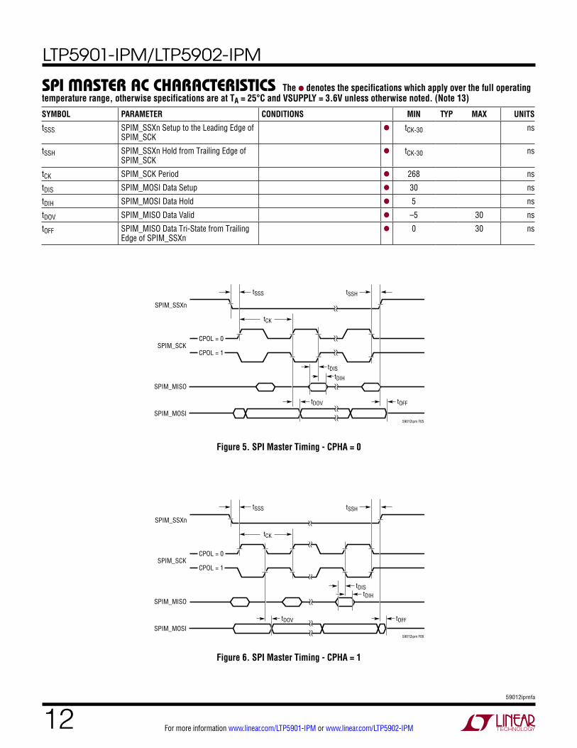
spi MasTer ac characTerisTics The l denotes the specifications which apply over the full operating temperature range, otherwise specifications are at TA = 25°C and VSUPPLY = 3.6V unless otherwise noted. (Note 13)
SYMBOL PARAMETER CONDITIONS MIN TYP MAX UNITS
tSSS SPIM_SSXn Setup to the Leading Edge of SPIM_SCK
l tCK-30 ns
tSSH SPIM_SSXn Hold from Trailing Edge of SPIM_SCK
l tCK-30 ns
tCK SPIM_SCK Period l 268 ns
tDIS SPIM_MOSI Data Setup l 30 ns
tDIH SPIM_MOSI Data Hold l 5 ns
tDOV SPIM_MISO Data Valid l –5 30 ns
tOFF SPIM_MISO Data Tri-State from Trailing Edge of SPIM_SSXn
For more information www.linear.com/LTP5901-IPM or www.linear.com/LTP5902-IPM
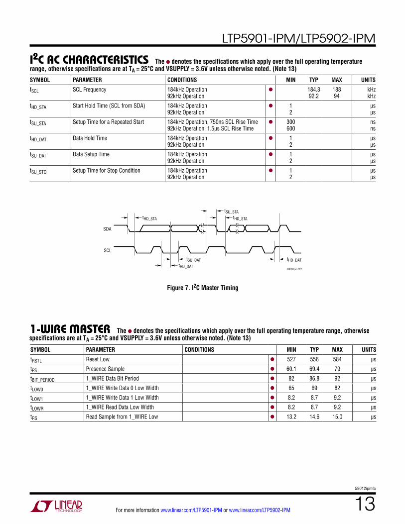
i2c ac characTerisTics The l denotes the specifications which apply over the full operating temperature range, otherwise specifications are at TA = 25°C and VSUPPLY = 3.6V unless otherwise noted. (Note 13)
SYMBOL PARAMETER CONDITIONS MIN TYP MAX UNITS
fSCL SCL Frequency 184kHz Operation 92kHz Operation
l 184.3 92.2
188 94
kHz kHz
tHD_STA Start Hold Time (SCL from SDA) 184kHz Operation 92kHz Operation
l 1 2
µs µs
tSU_STA Setup Time for a Repeated Start 184kHz Operation, 750ns SCL Rise Time 92kHz Operation, 1.5µs SCL Rise Time
l 300 600
ns ns
tHD_DAT Data Hold Time 184kHz Operation 92kHz Operation
l 1 2
µs µs
tSU_DAT Data Setup Time 184kHz Operation 92kHz Operation
l 1 2
µs µs
tSU_STO Setup Time for Stop Condition 184kHz Operation 92kHz Operation
l 1 2
µs µs
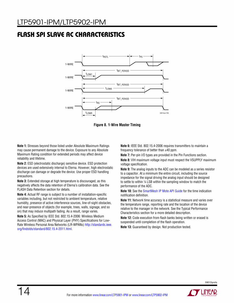
1-wire MasTer The l denotes the specifications which apply over the full operating temperature range, otherwise specifications are at TA = 25°C and VSUPPLY = 3.6V unless otherwise noted. (Note 13)
SYMBOL PARAMETER CONDITIONS MIN TYP MAX UNITS
tRSTL Reset Low l 527 556 584 µs
tPS Presence Sample l 60.1 69.4 79 µs
tBIT_PERIOD 1_WIRE Data Bit Period l 82 86.8 92 µs
tLOW0 1_WIRE Write Data 0 Low Width l 65 69 82 µs
tLOW1 1_WIRE Write Data 1 Low Width l 8.2 8.7 9.2 µs
tLOWR 1_WIRE Read Data Low Width l 8.2 8.7 9.2 µs
tRS Read Sample from 1_WIRE Low l 13.2 14.6 15.0 µs
For more information www.linear.com/LTP5901-IPM or www.linear.com/LTP5902-IPM
Note 1: Stresses beyond those listed under Absolute Maximum Ratings may cause permanent damage to the device. Exposure to any Absolute Maximum Rating condition for extended periods may affect device reliability and lifetime.Note 2: ESD (electrostatic discharge) sensitive device. ESD protection devices are used extensively internal to Eterna. However, high electrostatic discharge can damage or degrade the device. Use proper ESD handling precautions.Note 3: Extended storage at high temperature is discouraged, as this negatively affects the data retention of Eterna’s calibration data. See the FLASH Data Retention section for details.Note 4: Actual RF range is subject to a number of installation-specific variables including, but not restricted to ambient temperature, relative humidity, presence of active interference sources, line-of-sight obstacles, and near-presence of objects (for example, trees, walls, signage, and so on) that may induce multipath fading. As a result, range varies.Note 5: As Specified by IEEE Std. 802.15.4-2006: Wireless Medium Access Control (MAC) and Physical Layer (PHY) Specifications for Low-Rate Wireless Personal Area Networks (LR-WPANs) http://standards.ieee.org/findstds/standard/802.15.4-2011.html.
Note 6: IEEE Std. 802.15.4-2006 requires transmitters to maintain a frequency tolerance of better than ±40 ppm.Note 7: Per-pin I/O types are provided in the Pin Functions section.Note 8: VIH maximum voltage input must respect the VSUPPLY maximum voltage specification.Note 9: The analog inputs to the ADC can be modeled as a series resistor to a capacitor. At a minimum the entire circuit, including the source impedance for the signal driving the analog input should be designed to settle to within ¼ LSB within the sampling window to match the performance of the ADC.Note 10: See the SmartMesh IP Mote API Guide for the time indication notification definition.Note 11: Network time accuracy is a statistical measure and varies over the temperature range, reporting rate and the location of the device relative to the manager in the network. See the Typical Performance Characteristics section for a more detailed description.Note 12: Code execution from flash banks being written or erased is suspended until completion of the flash operation.Note 13: Guaranteed by design. Not production tested.
For more information www.linear.com/LTP5901-IPM or www.linear.com/LTP5902-IPM
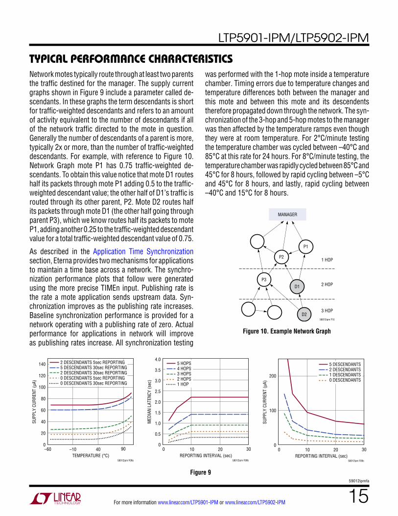
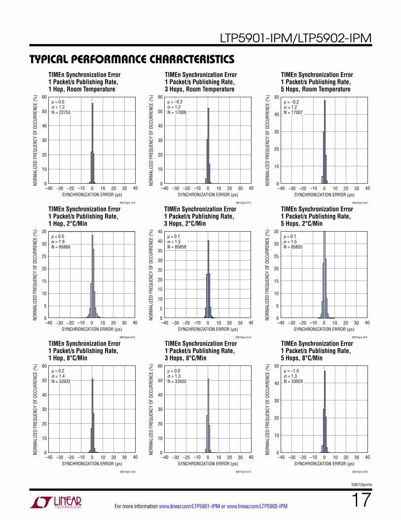
Network motes typically route through at least two parents the traffic destined for the manager. The supply current graphs shown in Figure 9 include a parameter called de-scendants. In these graphs the term descendants is short for traffic-weighted descendants and refers to an amount of activity equivalent to the number of descendants if all of the network traffic directed to the mote in question. Generally the number of descendants of a parent is more, typically 2x or more, than the number of traffic-weighted descendants. For example, with reference to Figure 10. Network Graph mote P1 has 0.75 traffic-weighted de-scendants. To obtain this value notice that mote D1 routes half its packets through mote P1 adding 0.5 to the traffic-weighted descendant value; the other half of D1’s traffic is routed through its other parent, P2. Mote D2 routes half its packets through mote D1 (the other half going through parent P3), which we know routes half its packets to mote P1, adding another 0.25 to the traffic-weighted descendant value for a total traffic-weighted descendant value of 0.75.
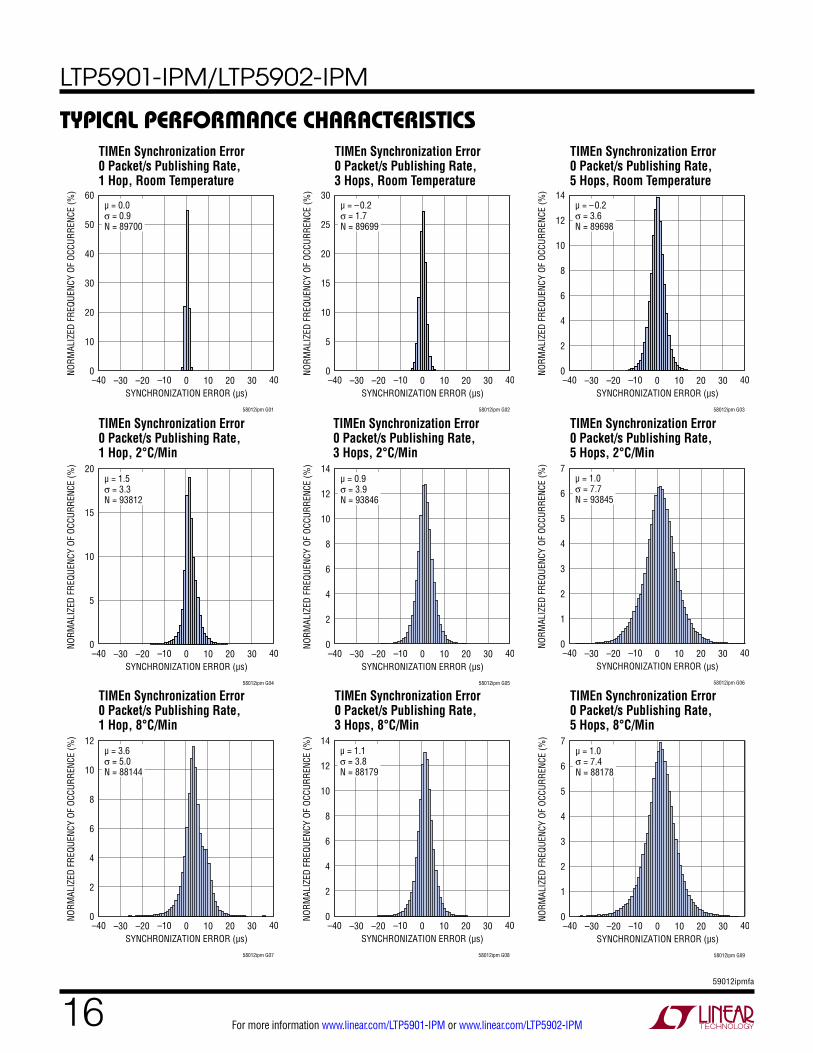
As described in the Application Time Synchronization section, Eterna provides two mechanisms for applications to maintain a time base across a network. The synchro-nization performance plots that follow were generated using the more precise TIMEn input. Publishing rate is the rate a mote application sends upstream data. Syn-chronization improves as the publishing rate increases. Baseline synchronization performance is provided for a network operating with a publishing rate of zero. Actual performance for applications in network will improve as publishing rates increase. All synchronization testing
was performed with the 1-hop mote inside a temperature chamber. Timing errors due to temperature changes and temperature differences both between the manager and this mote and between this mote and its descendents therefore propagated down through the network. The syn-chronization of the 3-hop and 5-hop motes to the manager was then affected by the temperature ramps even though they were at room temperature. For 2°C/minute testing the temperature chamber was cycled between –40°C and 85°C at this rate for 24 hours. For 8°C/minute testing, the temperature chamber was rapidly cycled between 85°C and 45°C for 8 hours, followed by rapid cycling between –5°C and 45°C for 8 hours, and lastly, rapid cycling between –40°C and 15°C for 8 hours.
For more information www.linear.com/LTP5901-IPM or www.linear.com/LTP5902-IPM
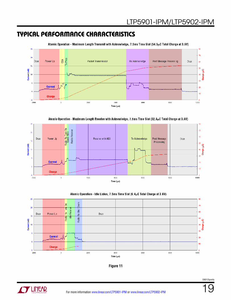
Typical perForMance characTerisTicsAs described in the SmartMesh Network Overview sec-tion, devices in network spend the vast majority of their time inactive in their lowest power state (doze). On a synchronous schedule a mote will wake to communicate with another mote. Regularly occurring sequences which wake, perform a significant function and return to sleep are considered atomic. These operations are considered atomic as the sequence of events can not be separated into smaller events while performing a useful function. For example, transmission of a packet over the radio is an atomic operation. Atomic operations may be characterized in either charge or energy. In a time slot where a mote successfully sends a packet, an atomic transmit includes setup prior to sending the message, sending the message, receiving the acknowledgment and the post processing needed as a result of the message being sent. Similarly in a time slot when a mote successfully receives a packet, an atomic receive includes setup prior to listening, listening
until the start of the packet transition, receiving the packet, sending the acknowledge and the post processing required due to the arrival of the packet.
To ensure reliability each mote in the network is provided multiple time slots for each packet it nominally will send and forward. The time slots are assigned to communicate upstream with at least two different motes. When combined with frequency hopping this provides temporal, spacial and spectral redundancy. Given this approach a mote will often listen for a message that it will never receive, since the time slot is not being used by the transmitting mote. It has already successfully transmitted the packet. Since typically 3 time slots are scheduled for every 1 packet to be sent or forwarded, motes will perform more of these atomic “idle listens” than atomic transmit or atomic receive sequences. Examples of transmit, receive and idle listen atomic operations are shown in Figure 11.
For more information www.linear.com/LTP5901-IPM or www.linear.com/LTP5902-IPM
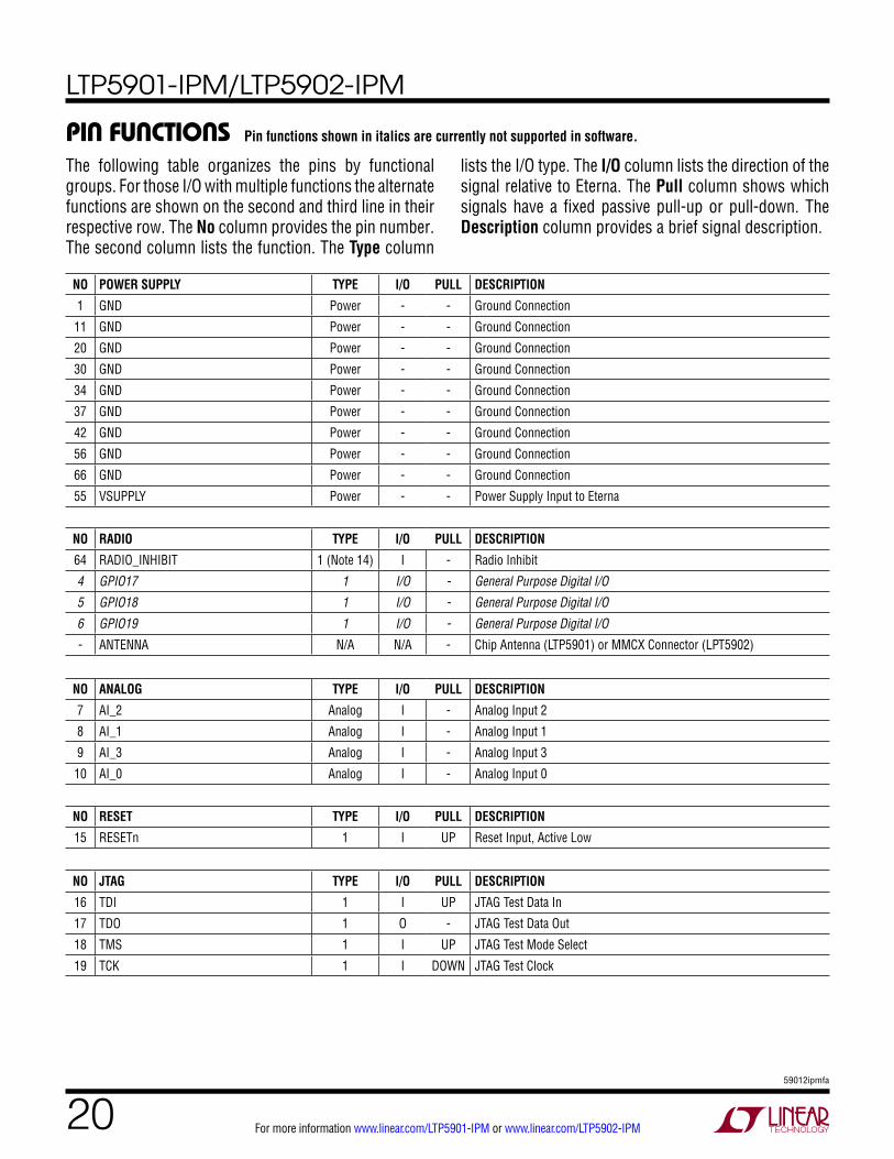
pin FuncTionsThe following table organizes the pins by functional groups. For those I/O with multiple functions the alternate functions are shown on the second and third line in their respective row. The No column provides the pin number. The second column lists the function. The Type column
lists the I/O type. The I/O column lists the direction of the signal relative to Eterna. The Pull column shows which signals have a fixed passive pull-up or pull-down. The Description column provides a brief signal description.
For more information www.linear.com/LTP5901-IPM or www.linear.com/LTP5902-IPM
pin FuncTionsVSUPPLY: System and I/O Power Supply. Provides power to the module. The digital-interface I/O voltages are also set by this voltage.
ANTENNA: Multiplexed Receiver Input and Transmitter Output Pin. The impedance presented to the MMCX con-nector should be 50Ω, single-ended with respect to ground.
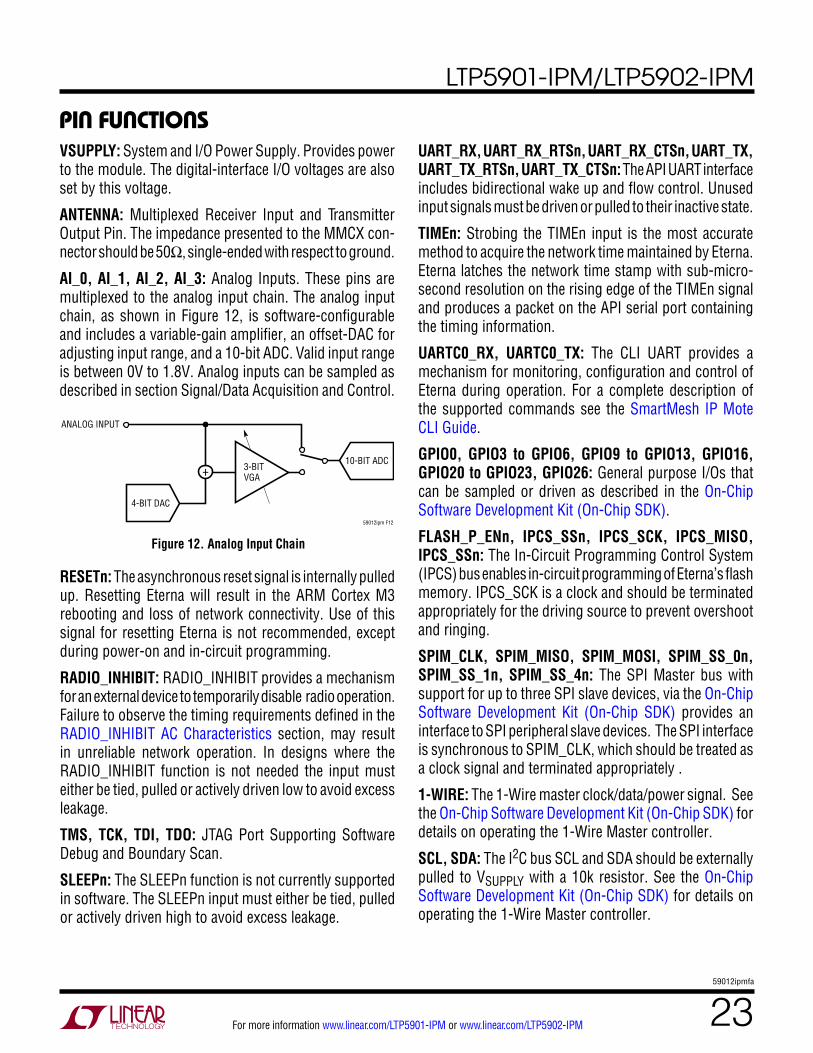
AI_0, AI_1, AI_2, AI_3: Analog Inputs. These pins are multiplexed to the analog input chain. The analog input chain, as shown in Figure 12, is software-configurable and includes a variable-gain amplifier, an offset-DAC for adjusting input range, and a 10-bit ADC. Valid input range is between 0V to 1.8V. Analog inputs can be sampled as described in section Signal/Data Acquisition and Control.
UART_RX, UART_RX_RTSn, UART_RX_CTSn, UART_TX, UART_TX_RTSn, UART_TX_CTSn: The API UART interface includes bidirectional wake up and flow control. Unused input signals must be driven or pulled to their inactive state.
TIMEn: Strobing the TIMEn input is the most accurate method to acquire the network time maintained by Eterna. Eterna latches the network time stamp with sub-micro-second resolution on the rising edge of the TIMEn signal and produces a packet on the API serial port containing the timing information.
UARTC0_RX, UARTC0_TX: The CLI UART provides a mechanism for monitoring, configuration and control of Eterna during operation. For a complete description of the supported commands see the SmartMesh IP Mote CLI Guide.
GPIO0, GPIO3 to GPIO6, GPIO9 to GPIO13, GPIO16, GPIO20 to GPIO23, GPIO26: General purpose I/Os that can be sampled or driven as described in the On-Chip Software Development Kit (On-Chip SDK).
FLASH_P_ENn, IPCS_SSn, IPCS_SCK, IPCS_MISO, IPCS_SSn: The In-Circuit Programming Control System (IPCS) bus enables in-circuit programming of Eterna’s flash memory. IPCS_SCK is a clock and should be terminated appropriately for the driving source to prevent overshoot and ringing.
SPIM_CLK, SPIM_MISO, SPIM_MOSI, SPIM_SS_0n, SPIM_SS_1n, SPIM_SS_4n: The SPI Master bus with support for up to three SPI slave devices, via the On-Chip Software Development Kit (On-Chip SDK) provides an interface to SPI peripheral slave devices. The SPI interface is synchronous to SPIM_CLK, which should be treated as a clock signal and terminated appropriately .
1-WIRE: The 1-Wire master clock/data/power signal. See the On-Chip Software Development Kit (On-Chip SDK) for details on operating the 1-Wire Master controller.
SCL, SDA: The I2C bus SCL and SDA should be externally pulled to VSUPPLY with a 10k resistor. See the On-Chip Software Development Kit (On-Chip SDK) for details on operating the 1-Wire Master controller.
Figure 12. Analog Input Chain
59012ipm F12
ANALOG INPUT
3-BITVGA+
4-BIT DAC
10-BIT ADC
RESETn: The asynchronous reset signal is internally pulled up. Resetting Eterna will result in the ARM Cortex M3 rebooting and loss of network connectivity. Use of this signal for resetting Eterna is not recommended, except during power-on and in-circuit programming.
RADIO_INHIBIT: RADIO_INHIBIT provides a mechanism for an external device to temporarily disable radio operation. Failure to observe the timing requirements defined in the RADIO_INHIBIT AC Characteristics section, may result in unreliable network operation. In designs where the RADIO_INHIBIT function is not needed the input must either be tied, pulled or actively driven low to avoid excess leakage.
TMS, TCK, TDI, TDO: JTAG Port Supporting Software Debug and Boundary Scan.
SLEEPn: The SLEEPn function is not currently supported in software. The SLEEPn input must either be tied, pulled or actively driven high to avoid excess leakage.
For more information www.linear.com/LTP5901-IPM or www.linear.com/LTP5902-IPM
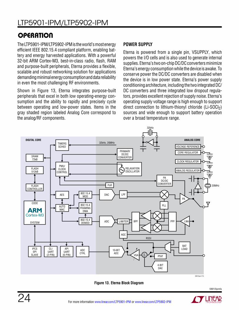
Figure 13. Eterna Block Diagram
4-BITDAC
VGA
BPF PPF
AGC
LPF
ADC
DAC
PLL
RSSI
LNA
PA
20MHz
32kHz
32kHz, 20MHz
PTAT
59012ipm F13
BATLOAD
LIMITER
VOLTAGE REFERENCE
ANALOG COREDIGITAL CORE
CORE REGULATOR
CLOCK REGULATOR
ANALOG REGULATOR
PADC/DC
CONVERTER
PRIMARYDC/DC
CONVERTER
RELAXATIONOSCILLATOR
PoR
TIMERSSCHED
SRAM72kB
FLASH512kB
FLASHCONTROLLER
CODE
AES
AUTOMAC
802.15.4MOD
802.15.4FRAMING
DMA
IPCSSPI
SLAVE
CLIUART
(2-PIN)
APIUART
(6-PIN)
ADCCTRL
802.15.4DEMODSYSTEM
PMU/CLOCK
CONTROL
10-BITADC
operaTionThe LTP5901-IPM/LTP5902-IPM is the world’s most energy efficient IEEE 802.15.4 compliant platform, enabling bat-tery and energy harvested applications. With a powerful 32-bit ARM Cortex-M3, best-in-class radio, flash, RAM and purpose-built peripherals, Eterna provides a flexible, scalable and robust networking solution for applications demanding minimal energy consumption and data reliability in even the most challenging RF environments.
Shown in Figure 13, Eterna integrates purpose-built peripherals that excel in both low operating-energy con-sumption and the ability to rapidly and precisely cycle between operating and low-power states. Items in the gray shaded region labeled Analog Core correspond to the analog/RF components.
POWER SUPPLY
Eterna is powered from a single pin, VSUPPLY, which powers the I/O cells and is also used to generate internal supplies. Eterna’s two on-chip DC/DC converters minimize Eterna’s energy consumption while the device is awake. To conserve power the DC/DC converters are disabled when the device is in low power state. Eterna’s power supply conditioning architecture, including the two integrated DC/DC converters and three integrated low dropout regula-tors, provides excellent rejection of supply noise. Eterna’s operating supply voltage range is high enough to support direct connection to lithium-thionyl chloride (Li-SOCl2) sources and wide enough to support battery operation over a broad temperature range.
For more information www.linear.com/LTP5901-IPM or www.linear.com/LTP5902-IPM
operaTionSUPPLY MONITORING AND RESET
Eterna integrates a Power-on Reset (PoR) circuit. As the RESETn input pin is nominally configured with an internal pull-up resistor, no connection is required. For a graceful shutdown, the software and the networking layers should be cleanly halted via API commands prior to assertion of the RESETn pin. See the SmartMesh IP Mote API Guide for details on the disconnect and reset commands. Eterna includes a soft brown-out monitor that fully protects the flash from corruption in the event that power is removed while writing to flash. Integrated flash supervisory func-tionality, in conjunction with a fault tolerant file system, yields a robust nonvolatile storage solution.
PRECISION TIMING
A major feature of Eterna over competing 802.15.4 prod-uct offerings is its low-power dedicated timing hardware and timing algorithms. This functionality provides timing precision two to three orders of magnitude better than any other low-power solution available at the time of publication. Improved timing accuracy allows motes to minimize the amount of radio listening time required to ensure packet reception thereby lowering even further the power consumed by SmartMesh networks. Eterna’s patented timing hardware and timing algorithms provide superior performance over rapid temperature changes, further differentiating Eterna’s reliability when compared with other wireless products. In addition, precise timing enables networks to reduce spectral dead time, increasing total network throughput.
APPLICATION TIME SYNCHRONIzATION
In addition to coordinating time slots across the network, which is transparent to the user, Eterna’s timing manage-ment is used to support two mechanisms to share network time. Having an accurate, shared, network-wide time base enables events to be accurately time stamped or tasks to be performed in a synchronized fashion across a network. Eterna will send a time packet through its serial interface when one of the following occurs:
n Eterna receives an API request to read timen The TIMEn signal is asserted
The use of TIMEn has the advantage of being more accu-rate. The value of the timestamp is captured in hardware relative to the rising edge of TIMEn. If an API request is used, due to packet processing, the value of the timestamp may be captured several milliseconds after receipt of the packet due to packet processing. See the TIMEn AC Characteristics section for the time function’s definition and specifications.
TIME REFERENCES
Eterna includes three clock sources: an internal relaxation oscillator, a low power oscillator designed for a 32.768kHz crystal, and the radio reference oscillator designed for a 20MHz crystal.
Relaxation Oscillator
The relaxation oscillator is the primary clock source for Eterna, providing the clock for the CPU, memory subsystems, and all peripherals. The internal relaxation oscillator is dynamically calibrated to 7.3728 MHz. The internal relaxation oscillator typically starts up in a few μs, providing an expedient, low energy method for duty cycling between active and low power states. Quick start-up from the doze state, defined in the State Diagram section, allows Eterna to wake up and receive data over the UART and SPI interfaces by simply detecting activity on the appropriate signals.
32.768kHz Crystal
Once Eterna is powered up and the 32.768kHz crystal source has begun oscillating, the 32.768kHz crystal re-mains operational while in the active state, and is used as the timing basis when in doze state. See the State Diagram section for a description of Eterna’s operational states.
20MHz Crystal
The 20 MHz crystal source provides a frequency reference for the radio, and is automatically enabled and disabled by Eterna as needed.
For more information www.linear.com/LTP5901-IPM or www.linear.com/LTP5902-IPM
operaTionRADIO
Eterna includes the lowest power commercially available 2.4GHz IEEE 802.15.4e radio by a substantial margin. (Please refer to the Radio Specifications section for power consumption numbers.). Eterna’s integrated power amplifier is calibrated and temperature compensated to consistently provide power at a limit suitable for worldwide radio certifications. Additionally, Eterna uniquely includes a hardware-based autonomous MAC that handles precise sequencing of peripherals, including the transmitter, the receiver, and Advanced Encryption Standard (AES) pe-ripherals. The hardware-based autonomous Media Access Controller (MAC) minimizes CPU activity, thereby further decreasing power consumption.
UARTs
The principal network interface is through the application programming interface (API) UART. A Command-Line Interface (CLI) is also provided for support of test and debug functions. Both UARTs sense activity continuously, consuming virtually no power until data is transferred over the port and then automatically returning to their lowest power state after the conclusion of a transfer. The defini-tion for packet encoding on the API UART interface can be found in the SmartMesh IP Mote API Guide and the CLI command definitions can be found in the SmartMesh IP Mote CLI Guide.
API UART Protocol
The API UART protocol was created with the goal of supporting a wide range of companion Multipoint Control Units (MCUs) while reducing power consumption of the system. The receive half of the API UART protocol includes two additional signals in addition to UART_RX: UART_RX_RTSn and UART_RX_CTSn. The transmit half of the API UART protocol includes two additional signals in addition to UART_TX: UART_TX_RTSn and UART_TX_CTSn. The API UART protocol is referred to as Mode 4.
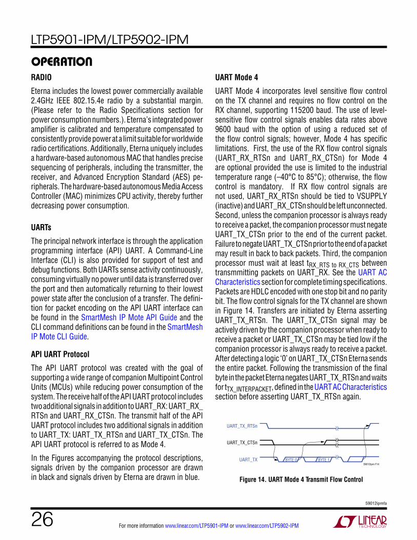
In the Figures accompanying the protocol descriptions, signals driven by the companion processor are drawn in black and signals driven by Eterna are drawn in blue. Figure 14. UART Mode 4 Transmit Flow Control
59012ipm F14UART_TX BYTE 0 BYTE 1
UART_TX_CTSn
UART_TX_RTSn
UART Mode 4
UART Mode 4 incorporates level sensitive flow control on the TX channel and requires no flow control on the RX channel, supporting 115200 baud. The use of level-sensitive flow control signals enables data rates above 9600 baud with the option of using a reduced set of the flow control signals; however, Mode 4 has specific limitations. First, the use of the RX flow control signals (UART_RX_RTSn and UART_RX_CTSn) for Mode 4 are optional provided the use is limited to the industrial temperature range (–40°C to 85°C); otherwise, the flow control is mandatory. If RX flow control signals are not used, UART_RX_RTSn should be tied to VSUPPLY (inactive) and UART_RX_CTSn should be left unconnected. Second, unless the companion processor is always ready to receive a packet, the companion processor must negate UART_TX_CTSn prior to the end of the current packet. Failure to negate UART_TX_CTSn prior to the end of a packet may result in back to back packets. Third, the companion processor must wait at least tRX_RTS to RX_CTS between transmmitting packets on UART_RX. See the UART AC Characteristics section for complete timing specifications. Packets are HDLC encoded with one stop bit and no parity bit. The flow control signals for the TX channel are shown in Figure 14. Transfers are initiated by Eterna asserting UART_TX_RTSn. The UART_TX_CTSn signal may be actively driven by the companion processor when ready to receive a packet or UART_TX_CTSn may be tied low if the companion processor is always ready to receive a packet. After detecting a logic ‘0’ on UART_TX_CTSn Eterna sends the entire packet. Following the transmission of the final byte in the packet Eterna negates UART_TX_RTSn and waits for tTX_INTERPACKET, defined in the UART AC Characteristics section before asserting UART_TX_RTSn again.
For more information www.linear.com/LTP5901-IPM or www.linear.com/LTP5902-IPM
operaTionFor details on the timing of the UART protocol, see the UART AC Characteristics section.
CLI UART
The Command Line Interface (CLI) UART port is a two wire protocol (TX and RX) that operates at a fixed 9600 baud rate with one stop bit and no parity. The CLI UART interface is intended to support command line instructions and response activity.
AUTONOMOUS MAC
Eterna was designed as a system solution to provide a reliable, ultralow power, and secure network. A reliable network capable of dynamically optimizing operation over changing environments requires solutions that are far too complex to completely support through hardware acceleration alone. As described in the Precision Timing section, proper time management is essential for optimizing a solution that is both low power and reliable. To address these requirements Eterna includes the autonomous MAC, which incorporates a coprocessor for controlling all of the time critical radio operations. The autonomous MAC provides two benefits: first, preventing variable software latency from affecting network timing and second, greatly reducing system power consumption by allowing the CPU to remain inactive during the majority of the radio activity. The autonomous MAC, provides software independent timing control of the radio and radio related functions, resulting in superior reliability and exceptionally low power.
SECURITY
Network security is an often overlooked component of a complete network solution. Proper implementation of se-curity protocols is significant in terms of both engineering effort and market value in an OEM product. Eterna system solutions provide a FIPS-197 validated encryption scheme that includes authentication and encryption at the MAC and network layers with separate keys for each mote. This not only yields end-to-end security, but if a mote is somehow compromised, communication from other motes is still secure. A mechanism for secure key exchange al-lows keys to be kept fresh. To prevent physical attacks, Eterna includes hardware support for electronically locking
devices, thereby preventing access to Eterna’s flash and RAM memory and thus the keys and code stored therein.
TEMPERATURE SENSOR
Eterna includes a calibrated temperature sensor on chip. The temperature readings are available locally through Eterna’s serial API, in addition to being available via the network manager. The performance characteristics of the temperature sensor can be found in the Temperature Sensor Characteristics section.
RADIO INHIBIT
The RADIO_INHIBIT input enables an external controller to temporarily disable the radio software drivers (for example, to take a sensor reading that is susceptible to radio interference). When RADIO_INHIBIT is asserted the software radio drivers will disallow radio operations including clear channel assessment, packet transmits, or packet receipts. If the radio is active in the current timeslot when RADIO_INHIBIT is asserted the radio will be diabled after the present operation completes. For details on the timing associated with RADIO_INHIBIT, see the RADIO_INHIBIT AC Characteristics section.
SOFTWARE INSTALLATION
Devices are supplied with the flash erased, requiring pro-gramming as part of the OEMs manufacturing procedure. The US Department of Commerce places restrictions on export of systems and software supporting encryption. All of Linear/Dust product software produced to date contains encryption and is subject to export regulations and may be provided only via MyLinear, https://www.linear.com/mylinear. Customers purchasing SmartMesh products will receive a certificate containing a registration key and registration instructions with their order. After registering with the key, customers will be able to download SmartMesh software images from MyLinear. Once registered, customers will receive automated e-mail notifications as software updates are made available.
Linear Technology offers the DC9010, in circuit program-mer for the Eterna based products. While the DC9010, is provided as a finished product, the design documents are provided as a reference for customers.
For more information www.linear.com/LTP5901-IPM or www.linear.com/LTP5902-IPM
operaTionOnce software has been loaded, devices can be configured via either the CLI or API ports. Configuration commands and settings are defined in SmartMesh IP Mote API Guide and SmartMesh IP Mote CLI Guide.
FLASH DATA RETENTION
Eterna contains internal flash (nonvolatile memory) to store calibration results, unique ID, configuration settings and software images. Flash retention over the operating temperature range. See Electrical Characteristics and Absolute Maximum Ratings sections.
Non destructive storage above the operating temperature range of –40°C to 85°C is possible; although, this may result in a degradation of retention characteristics.
The degradation in flash retention for temperatures >85°C can be approximated by calculating the dimensionless acceleration factor using the following equation.
AF = e
Eak
•
1TUSE+273
− 1TSTRESS+273
Where:
AF = acceleration factor
Ea = activation energy = 0.6eV
k = 8.625 • 10–5eV/°K
TUSE = is the specified temperature retention in °C
TSTRESS = actual storage temperature in °C
Example: Calculate the effect on retention when storing at a temperature of 105°C.
TSTRESS = 105°C
TUSE = 85°C
AF = 2.8
So the overall retention of the flash would be degraded by a factor of 2.8, reducing data retention from 20 years at 85°C to 7.1 years at 105°C.
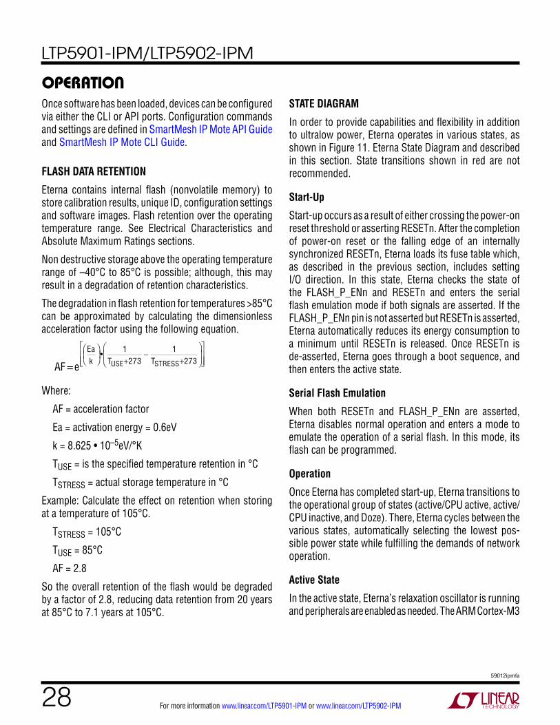
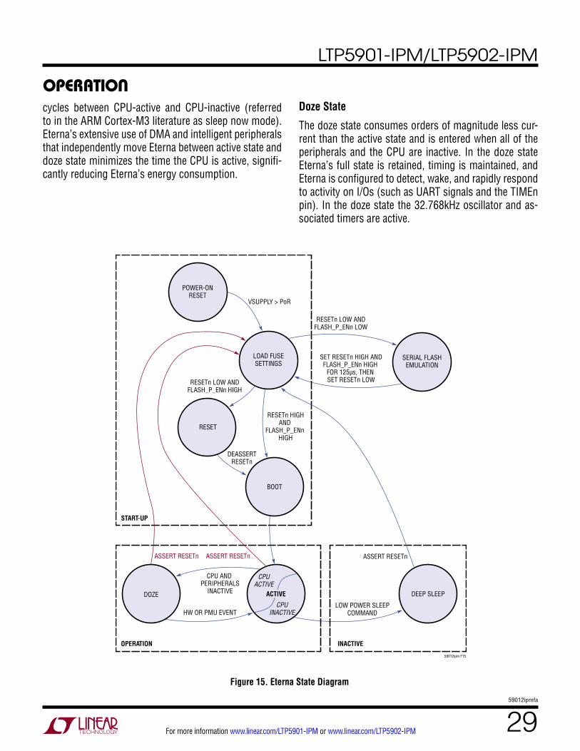
STATE DIAGRAM
In order to provide capabilities and flexibility in addition to ultralow power, Eterna operates in various states, as shown in Figure 11. Eterna State Diagram and described in this section. State transitions shown in red are not recommended.
Start-Up
Start-up occurs as a result of either crossing the power-on reset threshold or asserting RESETn. After the completion of power-on reset or the falling edge of an internally synchronized RESETn, Eterna loads its fuse table which, as described in the previous section, includes setting I/O direction. In this state, Eterna checks the state of the FLASH_P_ENn and RESETn and enters the serial flash emulation mode if both signals are asserted. If the FLASH_P_ENn pin is not asserted but RESETn is asserted, Eterna automatically reduces its energy consumption to a minimum until RESETn is released. Once RESETn is de-asserted, Eterna goes through a boot sequence, and then enters the active state.
Serial Flash Emulation
When both RESETn and FLASH_P_ENn are asserted, Eterna disables normal operation and enters a mode to emulate the operation of a serial flash. In this mode, its flash can be programmed.
Operation
Once Eterna has completed start-up, Eterna transitions to the operational group of states (active/CPU active, active/CPU inactive, and Doze). There, Eterna cycles between the various states, automatically selecting the lowest pos-sible power state while fulfilling the demands of network operation.
Active State
In the active state, Eterna’s relaxation oscillator is running and peripherals are enabled as needed. The ARM Cortex-M3
For more information www.linear.com/LTP5901-IPM or www.linear.com/LTP5902-IPM
Figure 15. Eterna State Diagram
LOAD FUSESETTINGS
RESETn LOW ANDFLASH_P_ENn HIGH
RESETn HIGHAND
FLASH_P_ENn HIGH
RESET
DEASSERTRESETn
CPU AND PERIPHERALS
INACTIVE
HW OR PMU EVENT
BOOT
START-UP
OPERATION INACTIVE
DOZE DEEP SLEEP
LOW POWER SLEEPCOMMAND
59012ipm F15
ASSERT RESETnASSERT RESETnASSERT RESETn
CPUACTIVE
CPUINACTIVE
POWER-ONRESET
RESETn LOW ANDFLASH_P_ENn LOW
SET RESETn HIGH ANDFLASH_P_ENn HIGH
FOR 125µs, THEN SET RESETn LOW
VSUPPLY > PoR
ACTIVE
SERIAL FLASHEMULATION
operaTioncycles between CPU-active and CPU-inactive (referred to in the ARM Cortex-M3 literature as sleep now mode). Eterna’s extensive use of DMA and intelligent peripherals that independently move Eterna between active state and doze state minimizes the time the CPU is active, signifi-cantly reducing Eterna’s energy consumption.
Doze State
The doze state consumes orders of magnitude less cur-rent than the active state and is entered when all of the peripherals and the CPU are inactive. In the doze state Eterna’s full state is retained, timing is maintained, and Eterna is configured to detect, wake, and rapidly respond to activity on I/Os (such as UART signals and the TIMEn pin). In the doze state the 32.768kHz oscillator and as-sociated timers are active.
For more information www.linear.com/LTP5901-IPM or www.linear.com/LTP5902-IPM
operaTionI2C MASTER
The I2C Master enables control of I2C slave devices, including support for clock stretching slaves. I2C Multi-master and bus arbitration protocols are not supported. For implementation details refer to the On-Chip Software Development Kit (On-Chip SDK).
SPI MASTER
The Eterna SPI master controller supports all configurations of clock polarity and phase, supporting shift clock frequen-cies of 460.8kHz, 921.6kHz, 1.8432MHz, or 3.6864MHz. In addition the SPI master controller can be configured to repetitively issue commands and capture the correspond-
ing output, enabling repetitive sampling of signals from a SPI ADC or SPI sensor based upon a clock reference of better than ±50ppm. For implementation details refer to the On-Chip Software Development Kit (On-Chip SDK).
1-WIRE MASTER
The Eterna 1-Wire Master controller supports the reset, presence detect, read and write 1-Wire protocol operations, incorporating an active pull-up. The active pull-up becomes active when the passive pull-up raises the voltage on the 1_WIRE pin nominally above 1.4V, driving the 1_WIRE signal as specified in Digital I/O Characteristics. For implementation details refer to the On-Chip Software Development Kit (On-Chip SDK).
For more information www.linear.com/LTP5901-IPM or www.linear.com/LTP5902-IPM
applicaTions inForMaTionMODES OF OPERATION
The SmartMesh IP Mote software can be operated in three distinct modes, namely, namely Slave, Master, and On-Chip SDK. Mode selection should be considered during the architecture/design phase of the development process.
Slave Mode
In Slave mode, the Eterna is connected to an external microprocessor through the API UART and is solely used as a networking device. None of the built in I/Os are ac-cessible in this mode. Refer to the SmartMesh IP User's Guide for more detailed information.
Master Mode
In Master mode, no external µProcessor is required and a limited set of functionality is made available with no pro-gramming required on the device. The following features are available
n On-Chip Temperature Sensorn 4 Analog Inputsn 4 Digital Inputsn 3 Digital Outputs
Refer to the SmartMesh IP User's Guide for more detailed information.
On-Chip SDK (OCSDK)
The SmartMesh IP On-Chip Software Development Kit (On-Chip SDK) enables development of C-code applications for execution on the LTC5800-IPM, running Micrium’s µCOS-II real-time operating system. With the On-Chip SDK, users may quickly and easily develop application code without the need for an external microprocessor.
Applications written within the On-Chip SDK may send and receive wireless messages through the mesh network; process data, such as statistical analysis; execute local decision-making and control; and manage the following peripherals:
n General Purpose Input-Output (GPIO) pinsn Analog-to-Digital Converter (ADC)n Universal Asynchronous Receiver/Transmitter
Network connectivity and quality of service is handled by the SmartMesh IP protocol stack. The SmartMesh IP stack comes as a pre-compiled library and delivers >99.999% data reliability while providing ultra low power operation.
REGULATORY AND STANDARDS COMPLIANCE
Radio Certification
The LTP5901 and LTP5902 have been certified under a single modular certification, with the module name of ETERNA2. Following the regulatory requirements pro-vided in the ETERNA2 User’s Guide enables customers to ship products in the supported geographies, by simply completing an unintentional radiator scan of the finished product(s). The ETERNA2 User’s Guide also provides the technical information needed to enable customers to further certify either the modules or products based upon the modules in geographies that have not or do not support modular certification.
Compliance to Restriction of Hazardous Substances (RoHS)
Restriction of Hazardous Substances 2 (RoHS 2) is a directive that places maximum concentration limits on the use of certain hazardous substances in electrical and electronic equipment. Linear Technology is committed to meeting the requirements of the European Community directive 2011/65/EU.
For more information www.linear.com/LTP5901-IPM or www.linear.com/LTP5902-IPM
applicaTions inForMaTion
relaTeD DocuMenTaTionTITLE LOCATION DESCRIPTION
SmartMesh IP Users Guide http://www.linear.com/docs/41880 Theory of operation for SmartMesh IP networks and motes
SmartMesh IP Mote API Guide http://www.linear.com/docs/41886 Definitions of the applications interface commands available over the API UART
SmartMesh IP Mote CLI Guide http://www.linear.com/docs/41885 Definitions of the command line interface commands available over the CLI UART
LTP5901 and LTP5902 Hardware Integration Guide
http://www.linear.com/docs/41877 Recommended practices for designing with the LTP5901 and LTP5902
ETERNA2 User’s Guide http://www.linear.com/docs/42916 The ETERNA2 module user’s guide includes certification requirements applicable to certified geographies and support documentation enabling customer certification in additional geographies for the LTP5901 and LTP5902
SmartMesh IP Tools Guide http://www.linear.com/docs/42453 The user’s guide for all IP related tools, and specifically the definition for the On-chip Application Protocol (OAP)
This product has been specifically designed to utilize RoHS-compliant materials and to eliminate or reduce the use of restricted materials to comply with 2011/65/EU.
The RoHS-compliant design features include:n RoHS-compliant solder for solder jointsn RoHS-compliant base metal alloysn RoHS-compliant precious metal platingn RoHS-compliant cable assemblies and connector
choicesn RoHS-compliant and 245°C reflow compatible
Note: Customers may elect to use certain types of lead-free solder alloys in accordance with the European Com-munity directive 2011/65/EU. Depending on the type of solder paste chosen, a corresponding process change to optimize reflow temperatures may be required.
SOLDERING INFORMATION
The LTP5901 and LTP5902 are suitable for both eutectic PbSn and RoHS-6 reflow. The maximum reflow solder-ing temperature is 260°C. A more detailed description of layout recommendations, assembly procedures and design considerations is included in the LTP5901 and LTP5902 Hardware Integration Guide.
For more information www.linear.com/LTP5901-IPM or www.linear.com/LTP5902-IPM
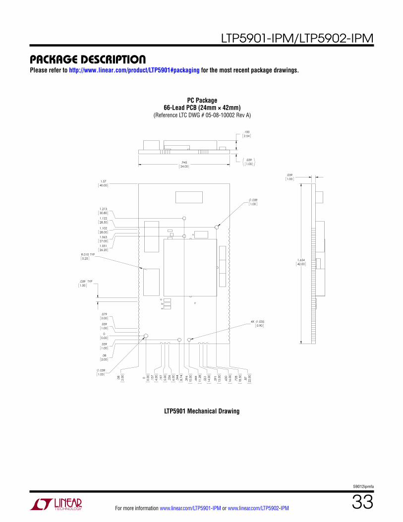
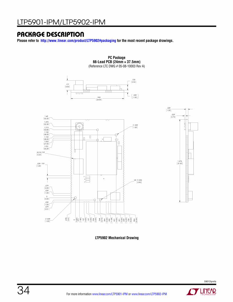
package DescripTionPlease refer to http://www.linear.com/product/LTP5901#packaging for the most recent package drawings.
PC Package66-Lead PCB (24mm × 42mm)
(Reference LTC DWG # 05-08-10002 Rev A)
R.0100.25
TYP
.0391.00
TYP
.0391.00
4X .0350.90
.0391.00
0
0.00
.0
82.
00
.1
574.
00
.1
975.
00
.2
366.
00
.3
448.
74
.4
4411
.28
.5
5114
.00
.5
9115
.00
.6
3016
.00
.8
722
.00
.7
2818
.50
.3
9410
.00
00.00
.082.00
.0391.00
.0391.00
.0792.00
1.10228.00
1.06327.00
1.03126.20
1.12228.50
1.21330.80
1.5740.00
.0391.00
1.65442.00
.1002.54
.0391.00
.945
24.00
A
1 2 3
B
APPD:
APPD:
PROD REL DATE:
PROJ MGR:
CHK:
DRN BY:
4 5 6DO NOT SCALE DWG OF
7 8SCALE
TITLEDIMENSIONS ARE IN INCHES
ENGRG MGR:
FINISH: DSIZE
±
MATERIAL:
TOLERANCES2 PLC
± ±
ANGLES3 PLC
APPROVALSDATE: UNLESS OTHERWISE SPECIFIED
PROJECTION
DWG NO. REV.
SHEET
A
C
D
1 2 3
C
4 5 6DESCRIPTIONREVZONE
D
APPROVEDDATE
7REVISIONS
8
RWB 1/27/13
061-0167 A1/1 1 1
.01 .005 0°30'CHECKER
APPD.
APPROVED
PROGRAM MGR:
A RELEASE PER ECO 001203 1/29/13 RWB
PCA OUTLINE DRAWING,LTP 5901
30695 HUNTWOOD AVE, HAYWARD, CA 94544
THE INFORMATION CONTAINED IN THIS DRAWING IS THE SOLE PROPERTY OF LINEAR INCORPORATED. ANY REPRODUCTION IN PART OR AS A WHOLE WITHOUT THE WRITTEN PERMISSION
OF LINEAR INCORPORATED IS PROHIBITED.
PROPRIETARY AND CONFIDENTIALLTP5901 Mechanical Drawing
For more information www.linear.com/LTP5901-IPM or www.linear.com/LTP5902-IPM
Information furnished by Linear Technology Corporation is believed to be accurate and reliable. However, no responsibility is assumed for its use. Linear Technology Corporation makes no representa-tion that the interconnection of its circuits as described herein will not infringe on existing patent rights.
revision hisToryREV DATE DESCRIPTION PAGE NUMBER
A 11/15 Updated ordering part numberAdded On-Chip SDK sectionAdded Software Installation section