IEEE Semiconductor Interface Specialists Conference Tutorial, Nov. 30th, 2011 Understanding the Nanoscale MOSFET Mark Lundstrom 1 Electrical and Computer Engineering and Network for Computational Nanotechnology Birck Nanotechnology Center Purdue University, West Lafayette, Indiana USA
Network for Computational Nanotechnology Birck Nanotechnology Center
Purdue University, West Lafayette, Indiana USA
2
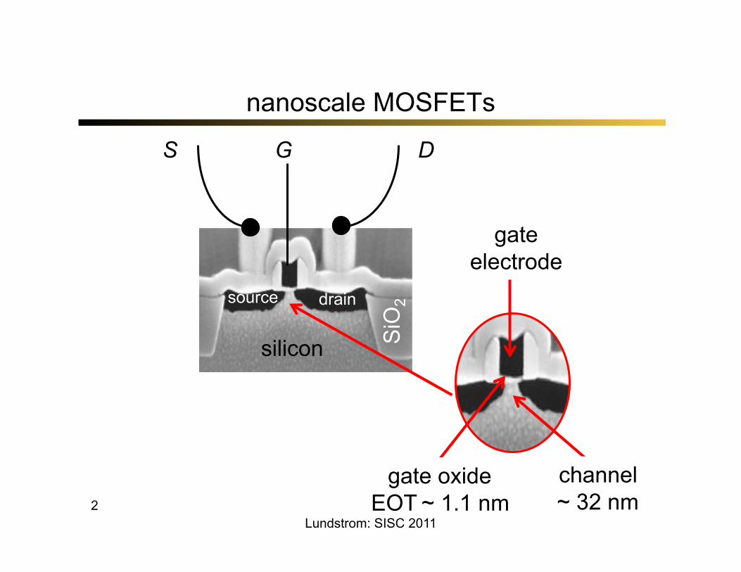
nanoscale MOSFETs
source drain
SiO
2
silicon
channel ~ 32 nm
gate oxide EOT ~ 1.1 nm
gate electrode
S G D
Lundstrom: SISC 2011
3
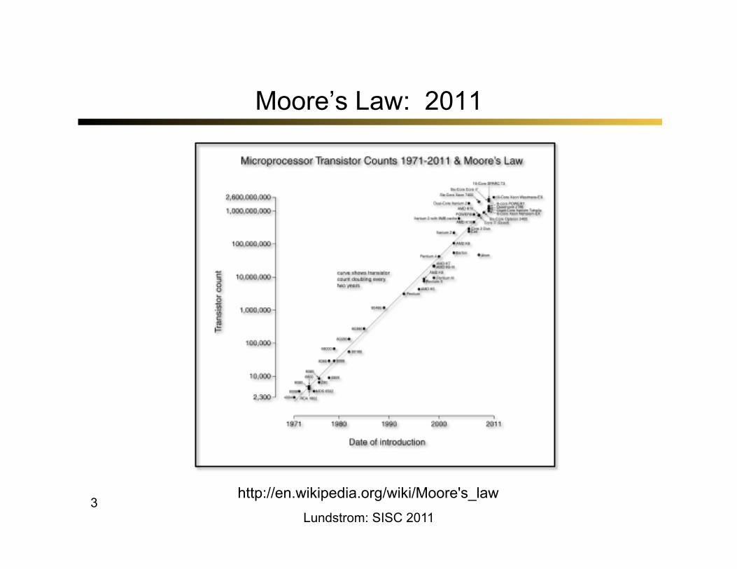
Moore’s Law: 2011
Lundstrom: SISC 2011
http://en.wikipedia.org/wiki/Moore's_law
4
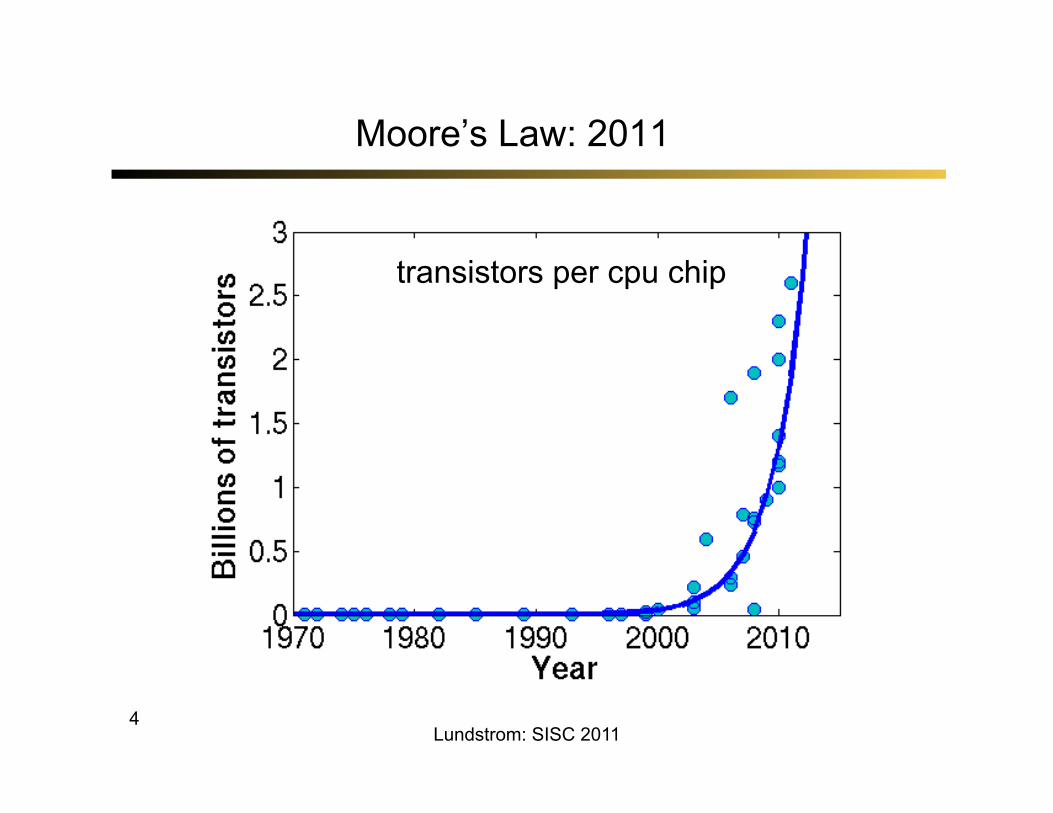
Moore’s Law: 2011
transistors per cpu chip
Lundstrom: SISC 2011
5
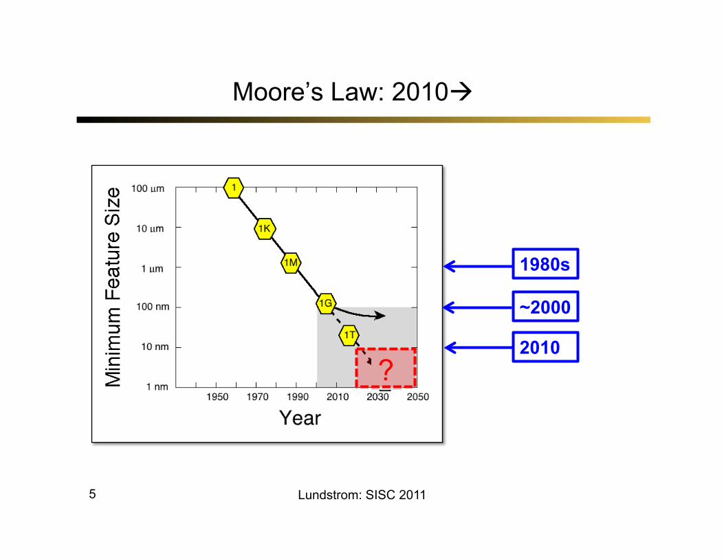
Moore’s Law: 2010
Lundstrom: SISC 2011
~2000
1980s
? 2010
6
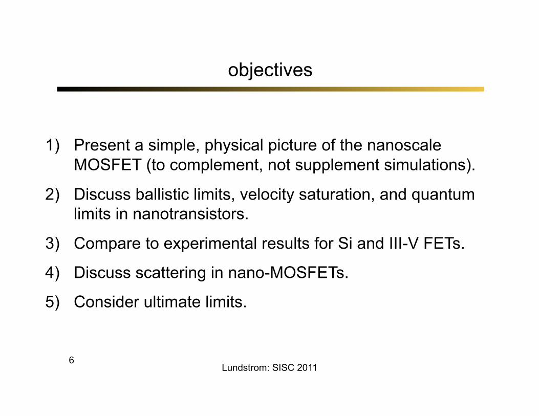
objectives
1) Present a simple, physical picture of the nanoscale MOSFET (to complement, not supplement simulations).
2) Discuss ballistic limits, velocity saturation, and quantum limits in nanotransistors.
3) Compare to experimental results for Si and III-V FETs.
4) Discuss scattering in nano-MOSFETs.
5) Consider ultimate limits.
Lundstrom: SISC 2011
7
outline
Lundstrom: SISC 2011
1) Introduction 2) Traditional approach 3) MOS electrostatics 4) The ballistic MOSFET 5) Comparison to experiments 6) Scattering in nano-MOSFETs 7) MOSFETs below 10 nm 8) Summary
This work is licensed under a Creative Commons Attribution-NonCommercial-ShareAlike 3.0 United States License. http://creativecommons.org/licenses/by-nc-sa/3.0/us/
8
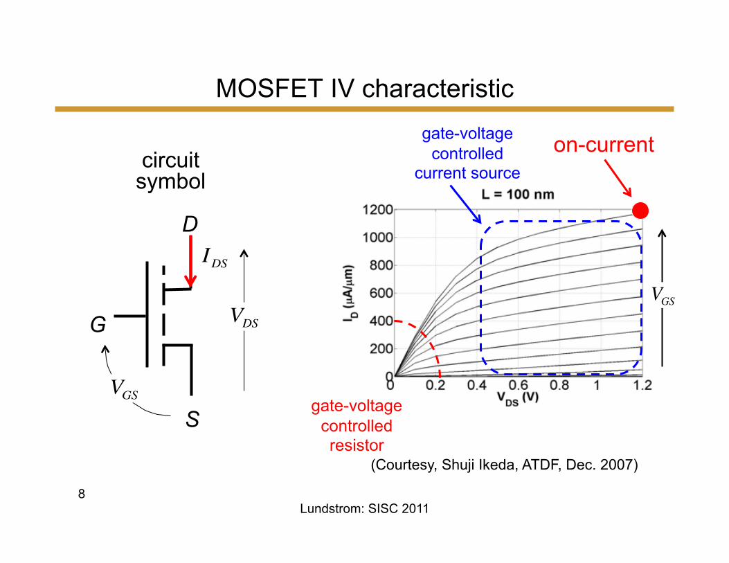
MOSFET IV characteristic
VGS
(Courtesy, Shuji Ikeda, ATDF, Dec. 2007)
S
D
G
circuit symbol
VDS
VGS
IDS
gate-voltage controlled resistor
Lundstrom: SISC 2011
gate-voltage controlled
current source on-current
9
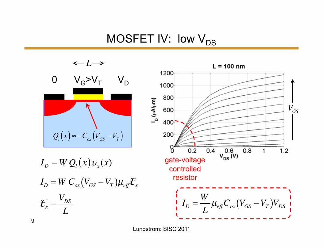
MOSFET IV: low VDS
VG>VT VD 0
ID =WQi x( )υx (x)
�
ID =W Cox VGS −VT( )µeffE x
Qi x( ) ≈ −Cox VGS −VT( )
�
ID = WL
µeffCox VGS −VT( )VDS
VGS
gate-voltage controlled resistor
Lundstrom: SISC 2011
�
E x = VDS
L
L
10
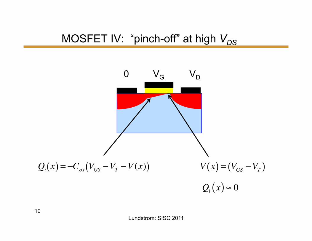
MOSFET IV: “pinch-off” at high VDS
VG VD 0
�
Qi x( ) = −Cox VGS −VT −V (x)( )
�
V x( ) = VGS −VT( )
Qi x( ) ≈ 0
Lundstrom: SISC 2011
11
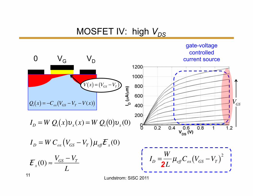
MOSFET IV: high VDS
VG VD 0
ID =W Cox VGS −VT( )µeffE x (0)
�
ID = WL
µeffCox VGS −VT( )22
E x (0) ≈
VGS −VTL
�
Qi x( ) = −Cox VGS −VT −V (x)( )�
V x( ) = VGS −VT( )
VGS
gate-voltage controlled
current source
�
ID =W Qi x( )υ x (x) =W Qi 0( )υ x (0)
Lundstrom: SISC 2011
12
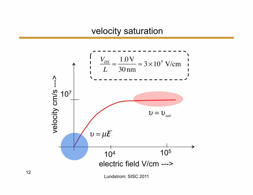
velocity saturation
electric field V/cm --->
velo
city
cm
/s --
->
107
104
�
υ = µE�
υ = υ sat
VDSL
≈ 1.0V30nm
≈ 3×10⁵ V/cm
105
Lundstrom: SISC 2011
13
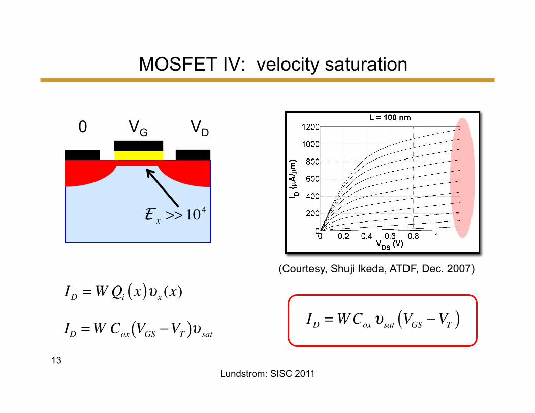
MOSFET IV: velocity saturation
VG VD 0
ID =WQi x( )υx (x)
�
ID =W Cox VGS −VT( )υ satID =WCoxυsat VGS −VT( )
E x >> 104
(Courtesy, Shuji Ikeda, ATDF, Dec. 2007)
Lundstrom: SISC 2011
µm( )
Velo
city
(cm
/s)
14
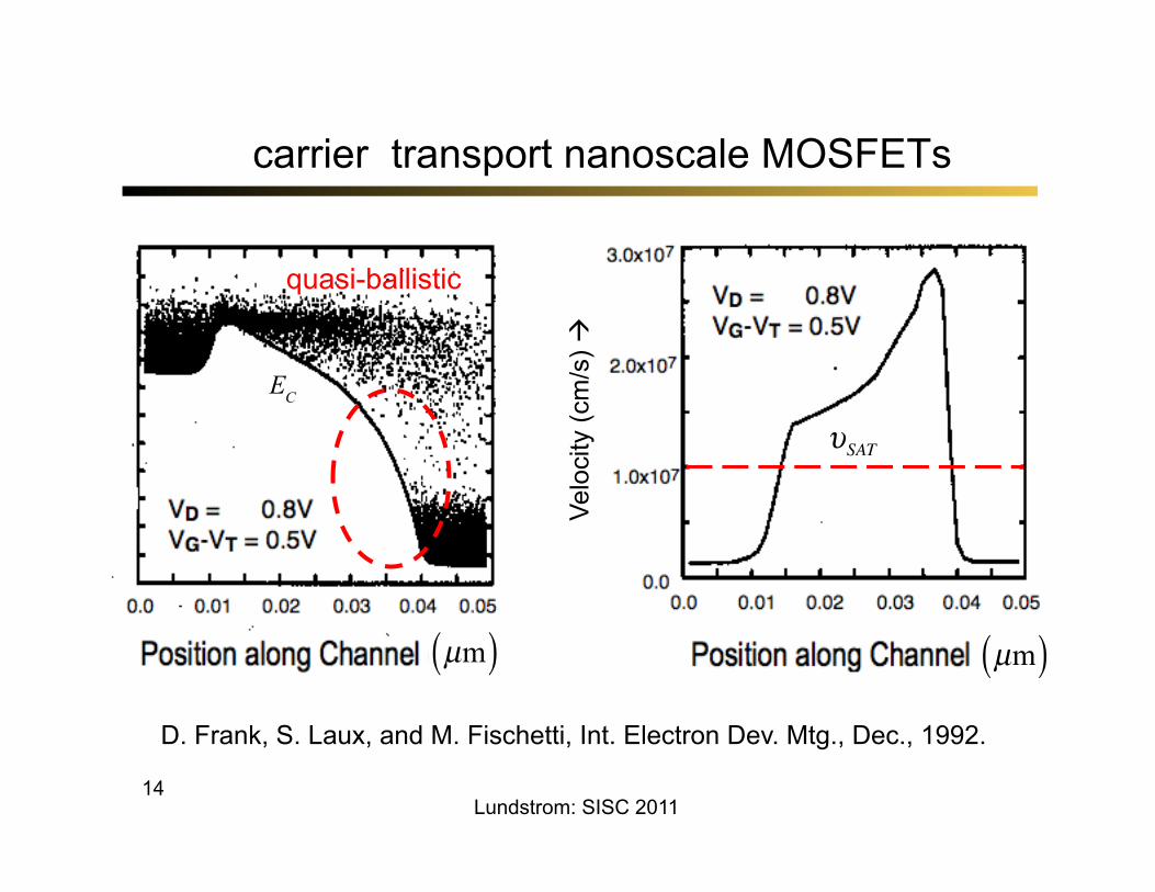
carrier transport nanoscale MOSFETs
υSAT
Lundstrom: SISC 2011
D. Frank, S. Laux, and M. Fischetti, Int. Electron Dev. Mtg., Dec., 1992.
µm( )
EC
quasi-ballistic
15
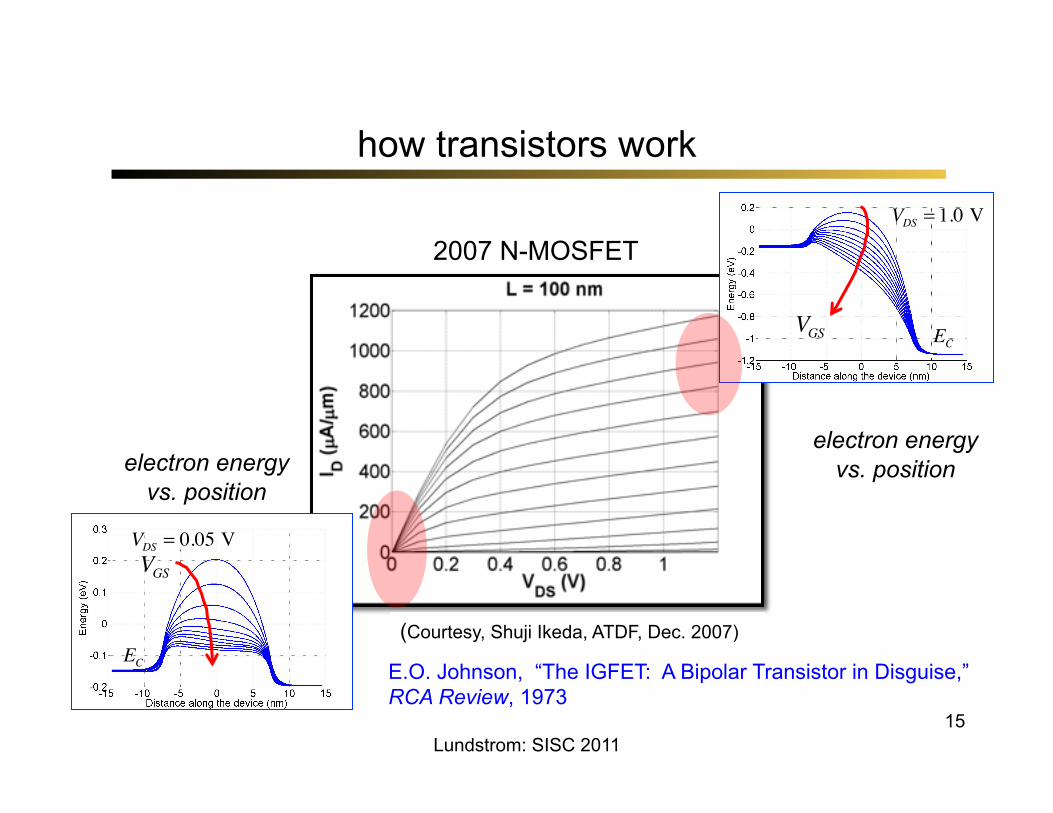
how transistors work
2007 N-MOSFET
electron energy vs. position
VDS = 0.05 VVGS
EC
(Courtesy, Shuji Ikeda, ATDF, Dec. 2007)
VDS = 1.0 V
VGS
electron energy vs. position
EC
E.O. Johnson, “The IGFET: A Bipolar Transistor in Disguise,” RCA Review, 1973
Lundstrom: SISC 2011
16
outline
Lundstrom: SISC 2011
1) Introduction 2) Traditional approach 3) MOS electrostatics 4) The ballistic MOSFET 5) Comparison to experiments 6) Scattering in nano-MOSFETs 7) MOSFETs below 10 nm 8) Summary
17
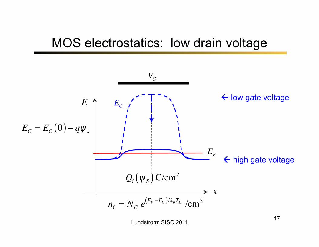
MOS electrostatics: low drain voltage
Lundstrom: SISC 2011
x
E
EF
EC
VG
Qi ψ S( )C/cm2
low gate voltage
high gate voltage
n0 = NC eEF −EC( ) kBTL /cm3
EC = EC 0( ) − qψ s
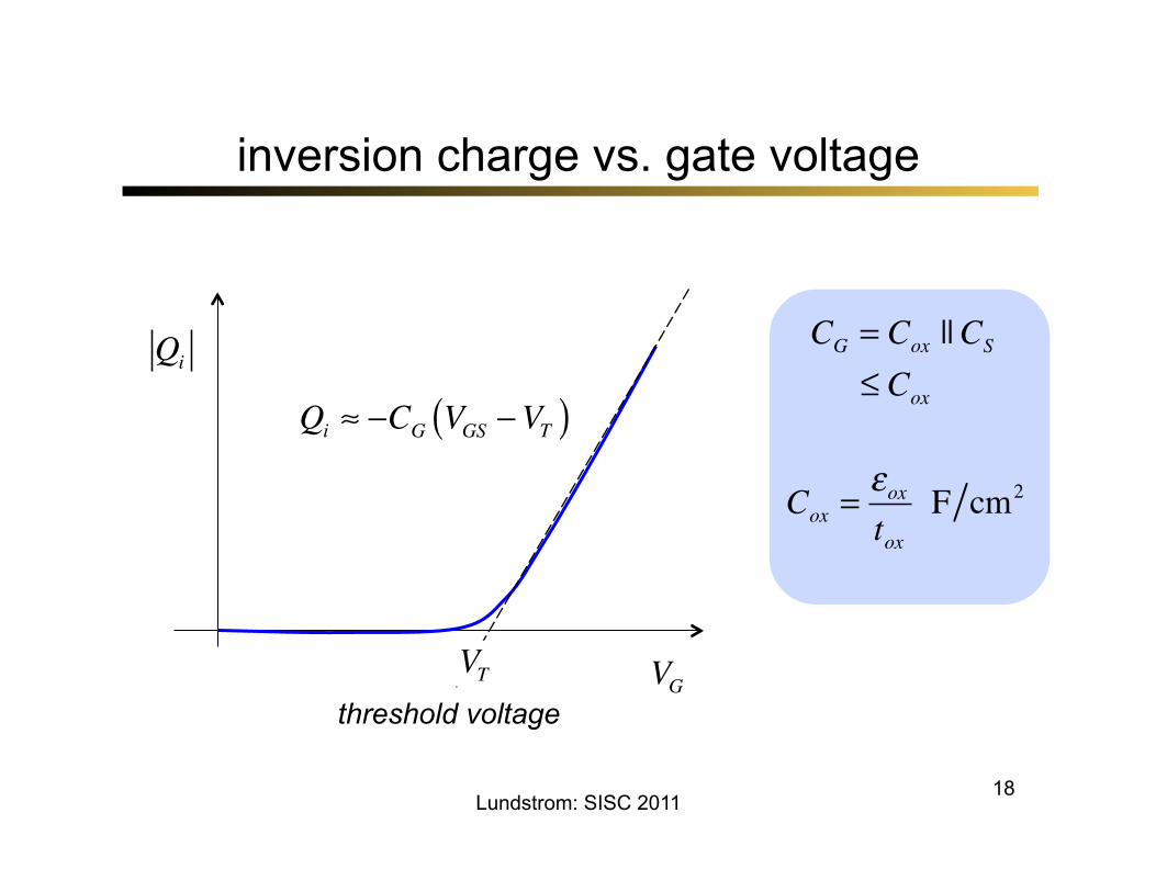
18
inversion charge vs. gate voltage
Lundstrom: SISC 2011
VG
Qi
Qi ≈ −CG VGS −VT( )
VTthreshold voltage
CG = Cox ||CS
≤ Cox
Cox =εoxtox
F cm2
19
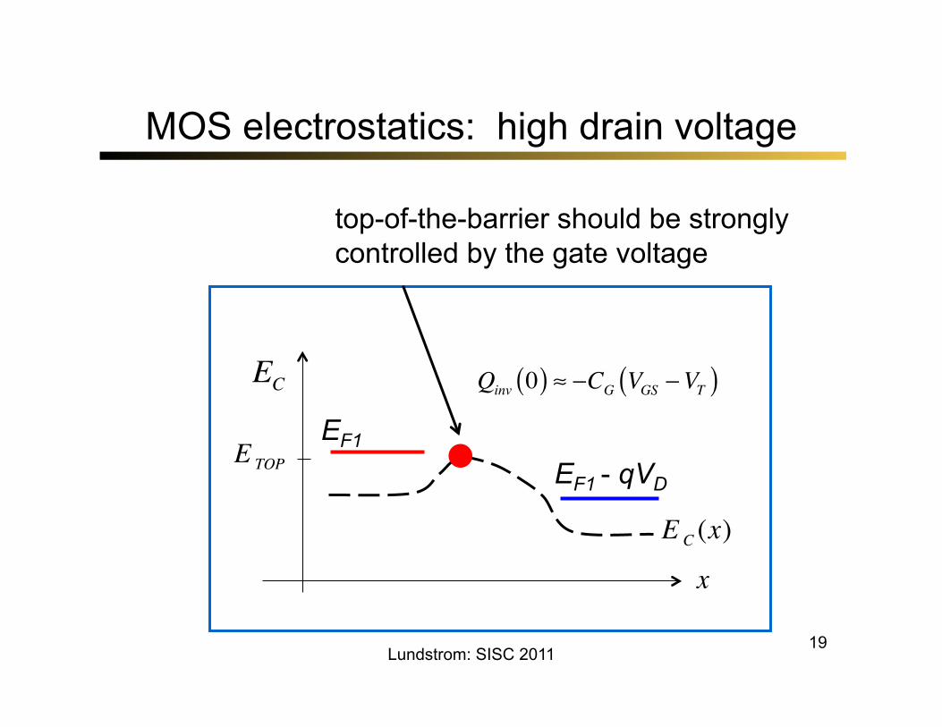
MOS electrostatics: high drain voltage
Lundstrom: SISC 2011
E TOP
EC
EF1 EF1 - qVD
E C (x)
x
top-of-the-barrier should be strongly controlled by the gate voltage
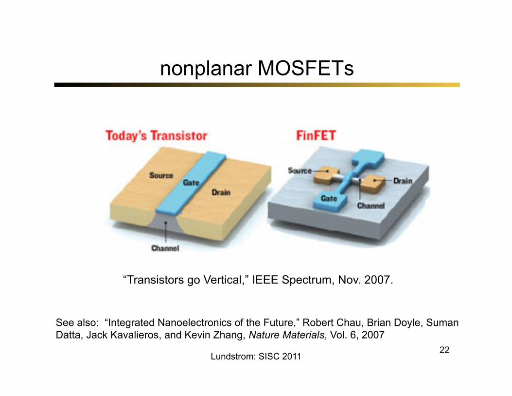
See also: “Integrated Nanoelectronics of the Future,” Robert Chau, Brian Doyle, Suman Datta, Jack Kavalieros, and Kevin Zhang, Nature Materials, Vol. 6, 2007
“Transistors go Vertical,” IEEE Spectrum, Nov. 2007.
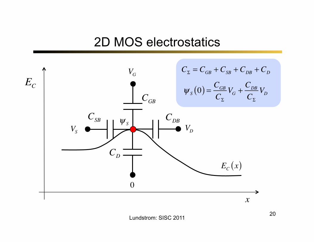
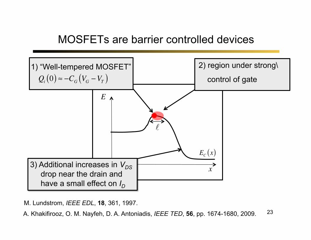
MOSFETs are barrier controlled devices
EC x( )
x
E
3) Additional increases in VDS drop near the drain and have a small effect on ID
A. Khakifirooz, O. M. Nayfeh, D. A. Antoniadis, IEEE TED, 56, pp. 1674-1680, 2009.
2) region under strong\
control of gate Qi 0( ) ≈ −CG VG −VT( )1) “Well-tempered MOSFET”
M. Lundstrom, IEEE EDL, 18, 361, 1997. 23
24
outline
Lundstrom: SISC 2011
1) Introduction 2) Traditional Approach 3) MOS electrostatics 4) The ballistic MOSFET 5) Comparison to experiments 6) Scattering in nano-MOSFETs 7) MOSFETs below 10 nm 8) Summary
25
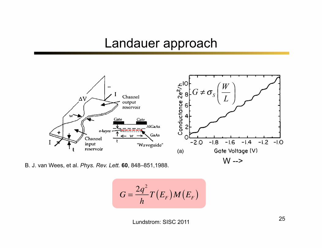
Landauer approach
Lundstrom: SISC 2011
W --> B. J. van Wees, et al. Phys. Rev. Lett. 60, 848–851,1988.
G =2q2
hT EF( )M EF( )
26
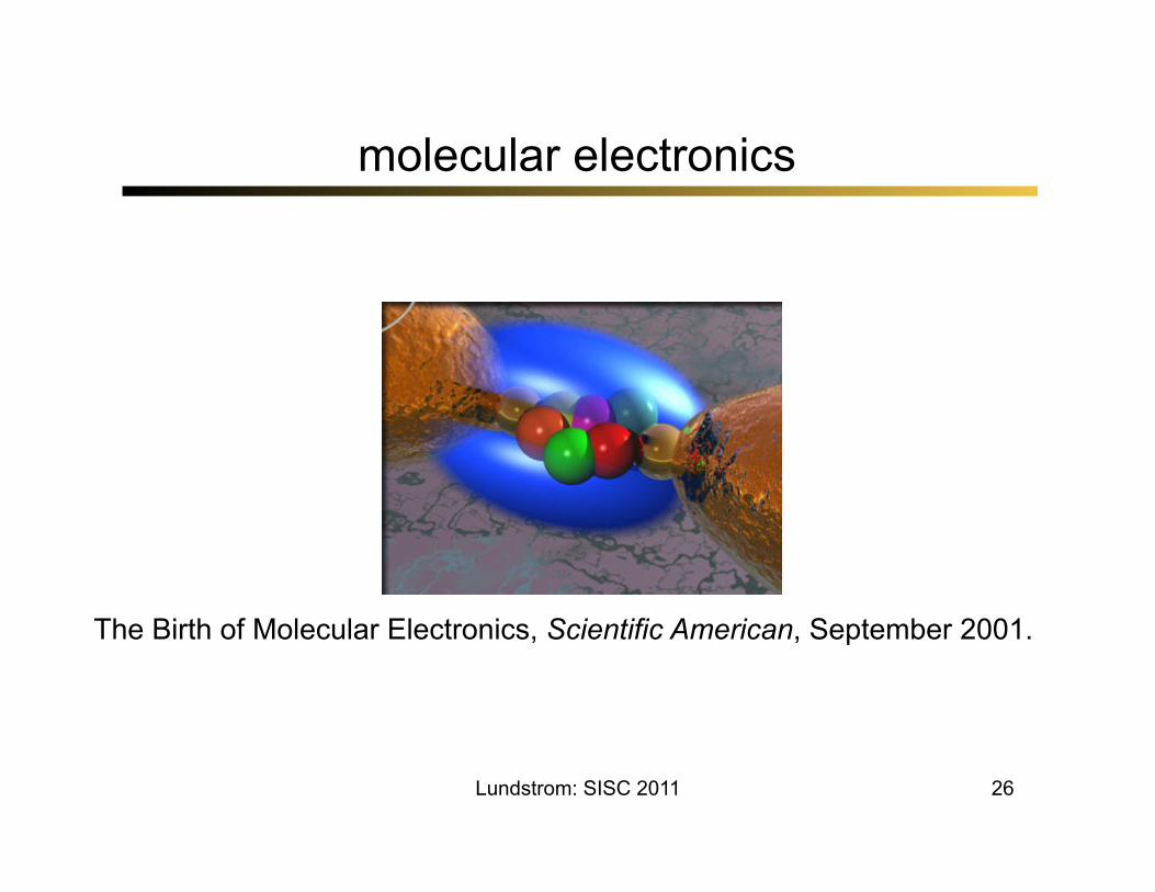
molecular electronics
Lundstrom: SISC 2011
The Birth of Molecular Electronics, Scientific American, September 2001.
27
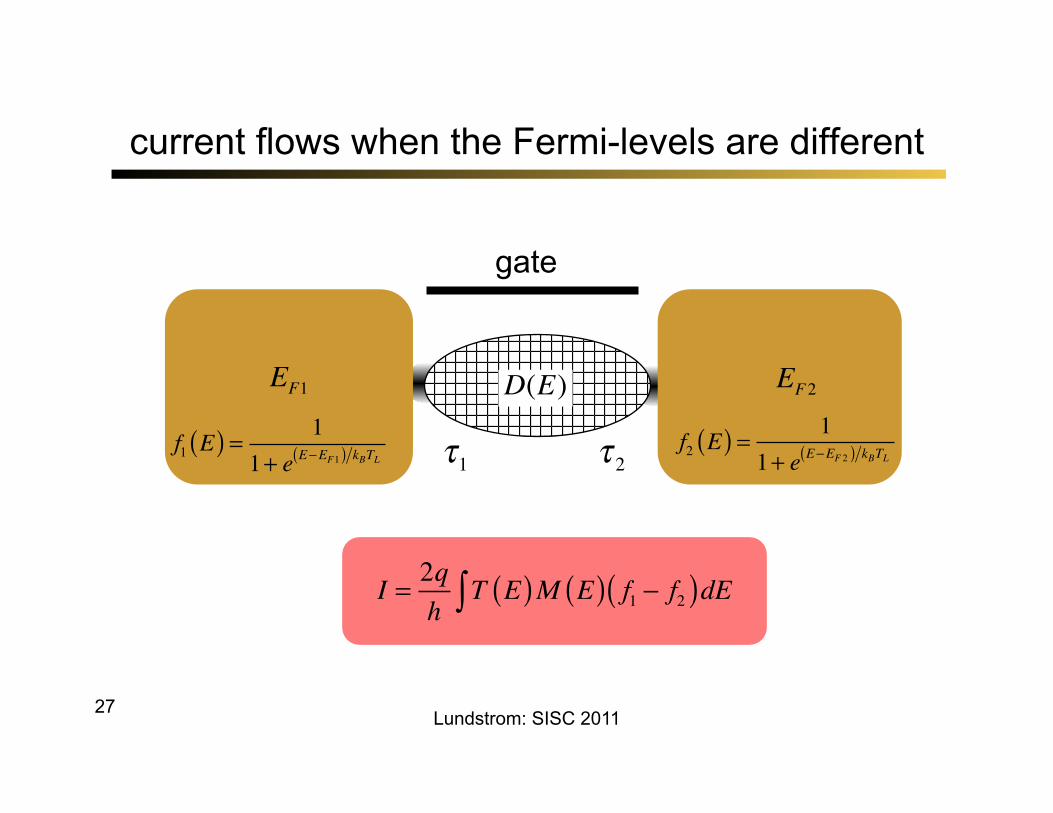
current flows when the Fermi-levels are different
D(E)
τ 2
EF1 EF2
τ1f1 E( ) = 11+ e E−EF1( ) kBTL
f2 E( ) = 11+ e E−EF 2( ) kBTL
gate
I = 2qh
T E( )M E( ) f1 − f2( )dE∫
Lundstrom: SISC 2011
28
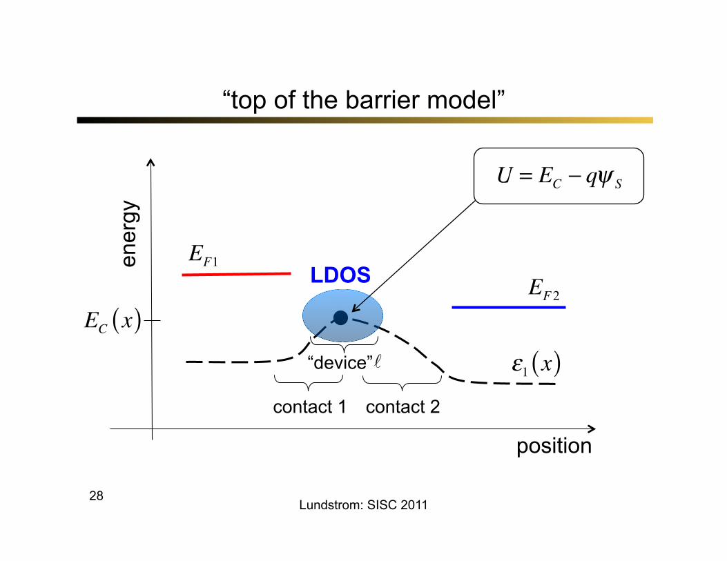
“top of the barrier model” en
ergy
position
contact 1 contact 2
“device”
LDOS
U = EC − qψ S
EF1
EF2
ε1 x( )EC x( )
Lundstrom: SISC 2011
29
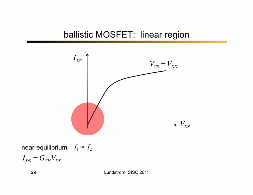
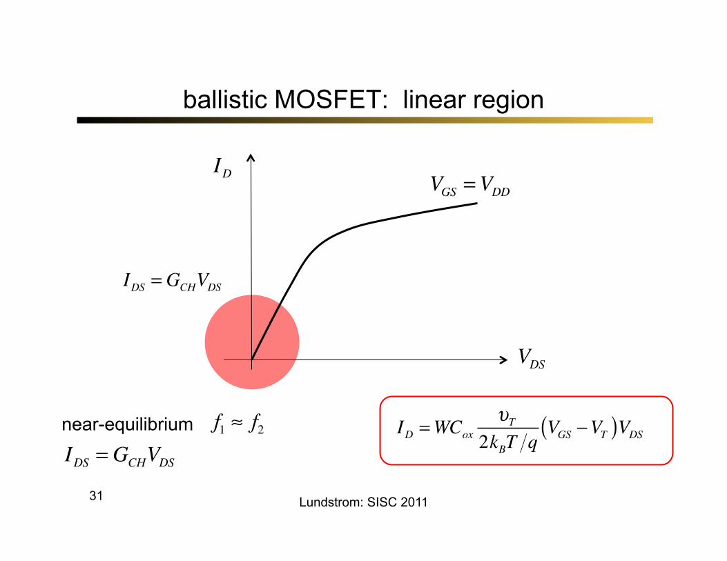
ballistic MOSFET: linear region
VDS
IDS VGS =VDD
Lundstrom: SISC 2011
near-equilibrium f1 ≈ f2IDS = GCHVDS
30
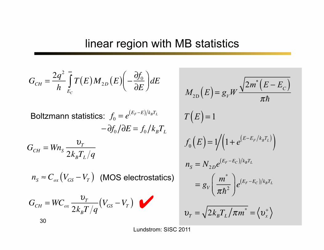
linear region with MB statistics
Lundstrom: SISC 2011
GCH = 2q2
hT E( )M 2D E( ) − ∂f0
∂E⎛⎝⎜
⎞⎠⎟ dE
EC
∞
∫ M2D E( ) = gVW
2m* E − EC( )π
T E( ) = 1
nS = N2DeEF −EC( ) kBTL
= gVm*
π2⎛⎝⎜
⎞⎠⎟e EF −EC( ) kBTL
GCH =WnSυT
2kBTL q
GCH =WCoxυT
2kBT qVGS −VT( )
nS ≈ Cox VGS −VT( ) (MOS electrostatics)
✔
f0 E( ) = 1 1+ e E−EF kBTL( )( )
υT = 2kBTL πm* = υx+
Boltzmann statistics: −∂f0 ∂E = f0 kBTL
f0 = eEF −E( ) kBTL
31
ballistic MOSFET: linear region
VDS
ID VGS =VDD
Lundstrom: SISC 2011
near-equilibrium f1 ≈ f2IDS = GCHVDS
IDS = GCHVDS
ID =WCoxυT
2kBT qVGS −VT( )VDS
32
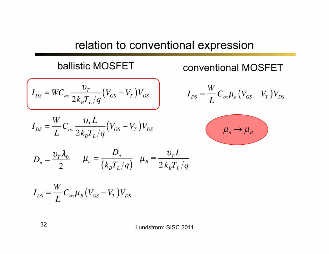
relation to conventional expression
Lundstrom: SISC 2011
IDS =WCoxυT
2kBTL qVGS −VT( )VDS
ballistic MOSFET conventional MOSFET
IDS =WLCoxµn VGS −VT( )VDS
IDS =WLCox
υT L2kBTL q
VGS −VT( )VDS
Dn =υTλ02
µn =Dn
kBTL q( )
IDS =WLCoxµB VGS −VT( )VDS
µB ≡υT L
2 kBTL q
µn → µB
33
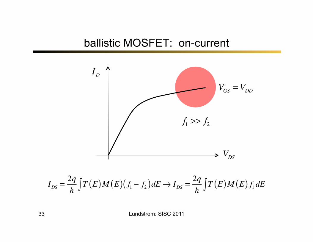
ballistic MOSFET: on-current
VDS
IDVGS =VDD
Lundstrom: SISC 2011
f1 >> f2
IDS =2qh
T E( )M E( ) f1 − f2( )dE∫ → IDS =2qh
T E( )M E( ) f1 dE∫
34
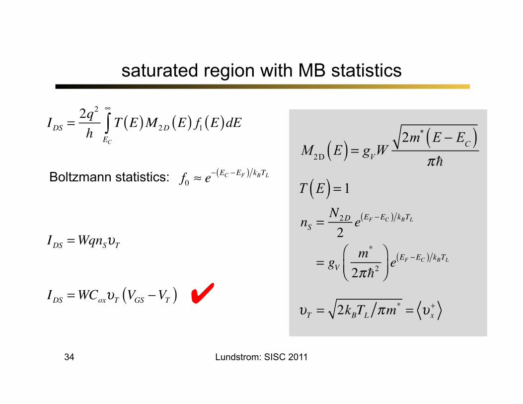
saturated region with MB statistics
Lundstrom: SISC 2011
IDS =2q2
hT E( )M 2D E( ) f1 E( )dE
EC
∞
∫
M2D E( ) = gVW
2m* E − EC( )π
T E( ) = 1
Boltzmann statistics: f0 ≈ e− EC −EF( ) kBTL
nS =N2D
2e EF −EC( ) kBTL
= gVm*
2π2⎛⎝⎜
⎞⎠⎟e EF −EC( ) kBTL
IDS =WqnSυT
υT = 2kBTL πm* = υx+
IDS =WCoxυT VGS −VT( ) ✔
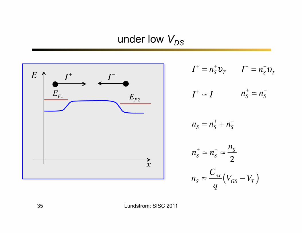
35
under low VDS
x
E
EF1 EF2
I +I + = nS
+υT
Lundstrom: SISC 2011
I −I − = nS
−υT
I + I − nS+ nS
−
nS = nS+ + nS
−
nS+ nS
− ≈ nS2
nS ≈Cox
qVGS −VT( )
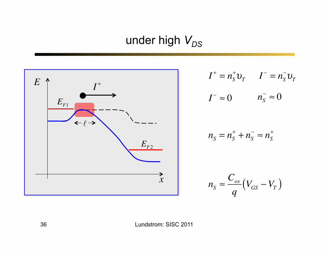
36
under high VDS
x
E
EF1
EF2
I +
Lundstrom: SISC 2011
I + = nS+υT I − = nS
−υT
I − ≈ 0 nS− ≈ 0
nS = nS+ + nS
− ≈ nS+
nS ≈Cox
qVGS −VT( )
37
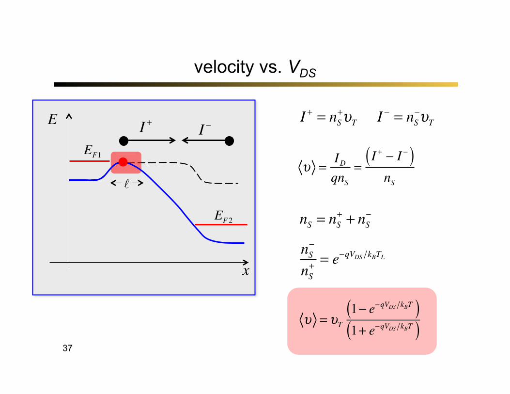
velocity vs. VDS
x
E
EF1
EF2
I + I −
υ =IDqnS
=I + − I −( )nS
I + = nS+υT I − = nS
−υT
nS = nS+ + nS
−
nS−
nS+ = e−qVDS kBTL
υ = υT
1− e−qVDS kBT( )1+ e−qVDS kBT( )
38
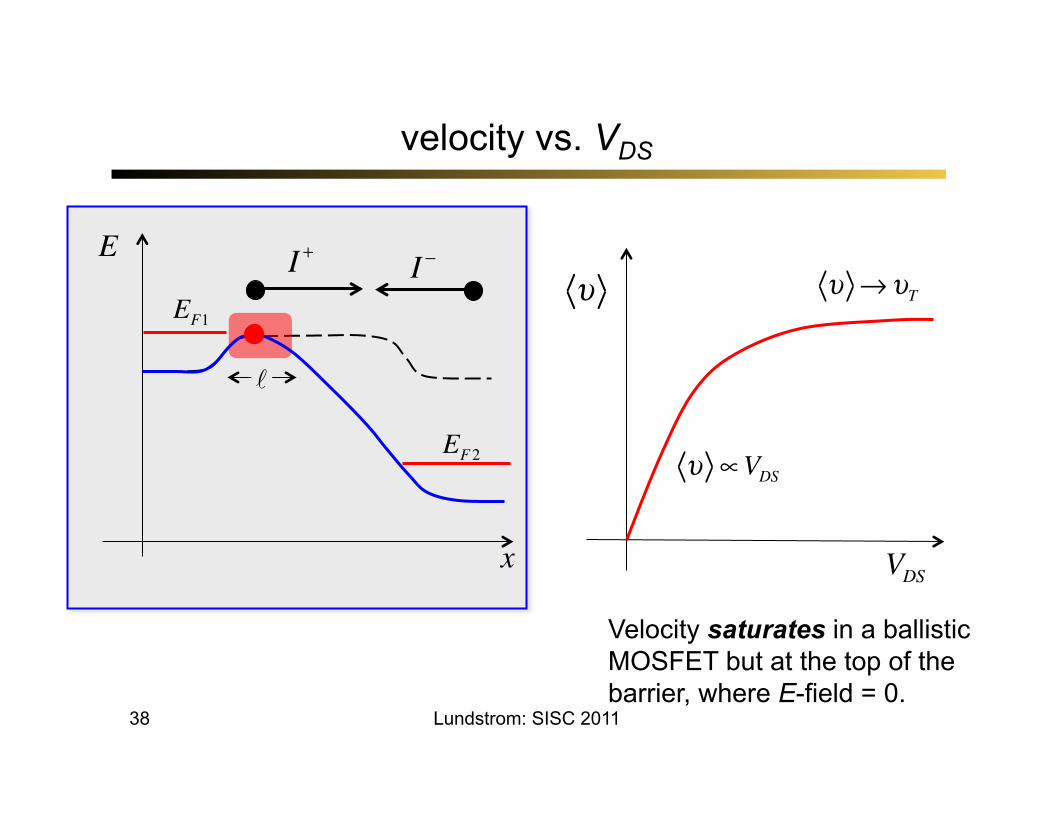
velocity vs. VDS
x
E
EF1
EF2
I + I −
υ ∝VDS
υ →υT
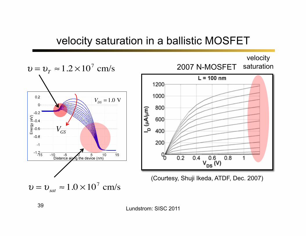
Velocity saturates in a ballistic MOSFET but at the top of the barrier, where E-field = 0.
Lundstrom: SISC 2011
υ
VDS
39
velocity saturation in a ballistic MOSFET
VDS = 1.0 V
VGS
(Courtesy, Shuji Ikeda, ATDF, Dec. 2007)
2007 N-MOSFET velocity
saturation
υ = υsat ≈ 1.0 ×107 cm/s
Lundstrom: SISC 2011
υ = υT ≈1.2 ×107 cm/s
40
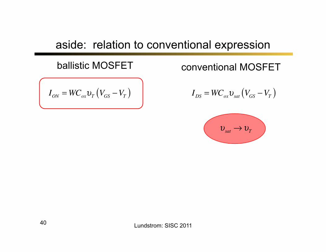
aside: relation to conventional expression
Lundstrom: SISC 2011
ION =WCoxυT VGS −VT( )
ballistic MOSFET conventional MOSFET
IDS =WCoxυsat VGS −VT( )
υsat →υT
41
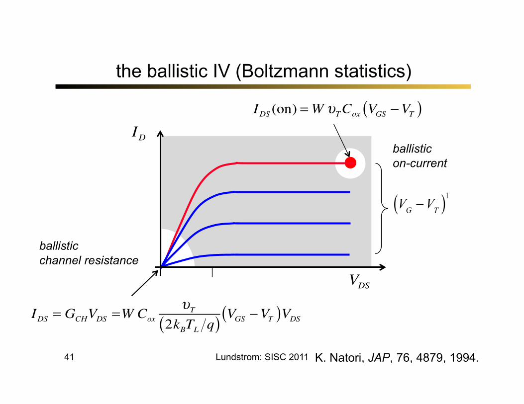
the ballistic IV (Boltzmann statistics)
VG −VT( )1
K. Natori, JAP, 76, 4879, 1994.
IDS (on) =W υTCox VGS −VT( )
IDS = GCHVDS =W CoxυT
2kBTL q( ) VGS −VT( )VDS
VDS
ID
ballistic channel resistance
ballistic on-current
Lundstrom: SISC 2011
42
outline
Lundstrom: SISC 2011
1) Introduction 2) Traditional Approach 3) MOS electrostatics 4) The ballistic MOSFET 5) Comparison to experiments 6) Scattering in nano-MOSFETs 7) MOSFETs below 10 nm 8) Summary
43
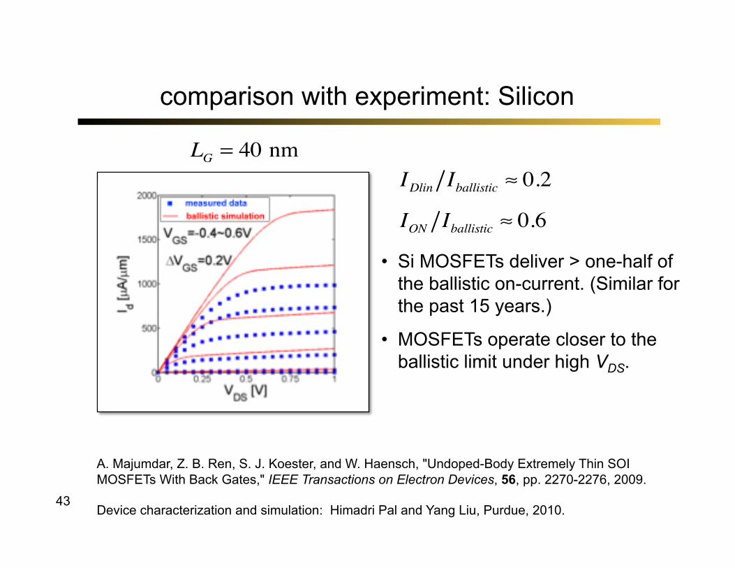
comparison with experiment: Silicon
A. Majumdar, Z. B. Ren, S. J. Koester, and W. Haensch, "Undoped-Body Extremely Thin SOI MOSFETs With Back Gates," IEEE Transactions on Electron Devices, 56, pp. 2270-2276, 2009.
Device characterization and simulation: Himadri Pal and Yang Liu, Purdue, 2010.
LG = 40 nm
ION Iballistic ≈ 0.6
IDlin Iballistic ≈ 0.2
• Si MOSFETs deliver > one-half of the ballistic on-current. (Similar for the past 15 years.)
• MOSFETs operate closer to the ballistic limit under high VDS.
44
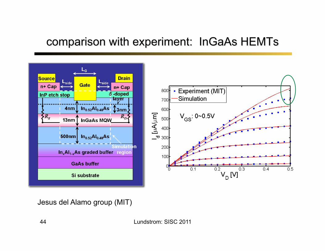
Jesus del Alamo group (MIT)
Lundstrom: SISC 2011
45
outline
Lundstrom: SISC 2011
1) Introduction 2) Traditional Approach 3) MOS electrostatics 4) The ballistic MOSFET 5) Comparison to experiments 6) Scattering in nano-MOSFETs 7) MOSFETs below 10nm 8) Summary
46
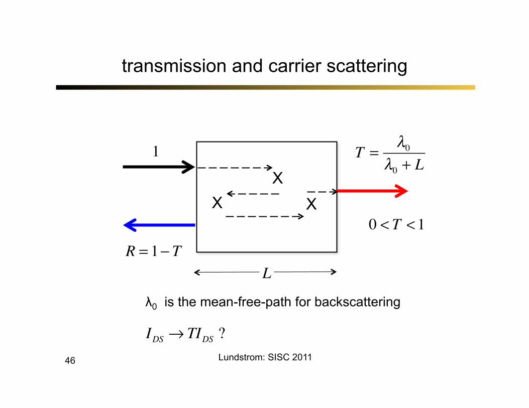
transmission and carrier scattering
T =λ0
λ0 + L
0 < T <1
R = 1− T
1
L
X X X
λ0 is the mean-free-path for backscattering
IDS → TIDS ?Lundstrom: SISC 2011
?
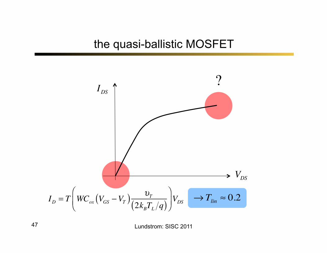
ID = T WCox VGS −VT( ) υT
2kBTL q( )⎛
⎝⎜⎞
⎠⎟VDS
47
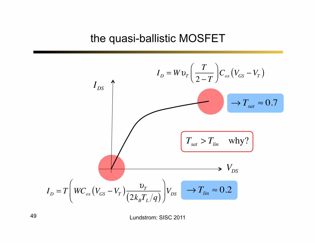
the quasi-ballistic MOSFET
VDS
IDS
→ Tlin ≈ 0.2
Lundstrom: SISC 2011
48
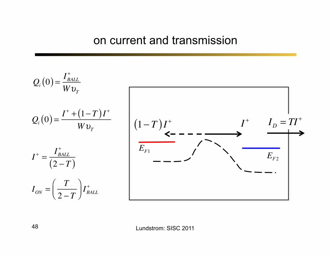
on current and transmission
Lundstrom: SISC 2011
ION =T2 − T
⎛⎝⎜
⎞⎠⎟IBALL+
EF1 EF2
ID = TI +I +1− T( ) I +Qi 0( ) = I + + 1−T( ) I +WυT
Qi 0( ) = IBALL+
WυT
I + =IBALL+
2 − T( )
ID =WυTT2 − T
⎛⎝⎜
⎞⎠⎟Cox VGS −VT( )
ID = T WCox VGS −VT( ) υT
2kBTL q( )⎛
⎝⎜⎞
⎠⎟VDS
49
the quasi-ballistic MOSFET
VDS
IDS→ Tsat ≈ 0.7
→ Tlin ≈ 0.2
Tsat > Tlin why?
Lundstrom: SISC 2011
50
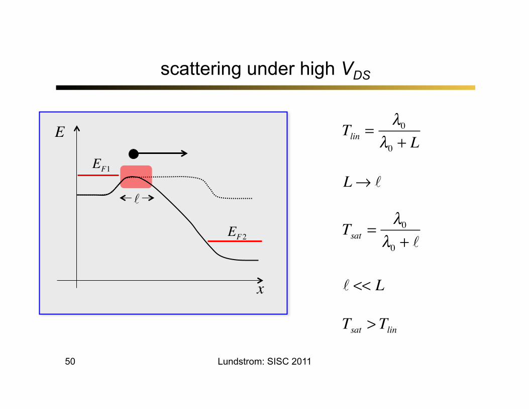
scattering under high VDS
x
E
EF1
EF2
Tsat =λ0
λ0 +
<< L
Tlin =λ0
λ0 + L
L→
Tsat > Tlin
Lundstrom: SISC 2011
51
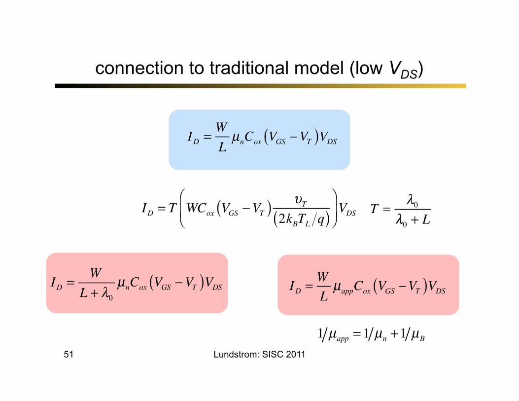
connection to traditional model (low VDS)
ID =WLµnCox VGS −VT( )VDS
ID =W
L + λ0µnCox VGS −VT( )VDS
ID = T WCox VGS −VT( ) υT
2kBTL q( )⎛
⎝⎜⎞
⎠⎟VDS
Lundstrom: SISC 2011
T =λ0
λ0 + L
ID = WLµappCox VGS −VT( )VDS
1 µapp = 1 µn +1 µB
52
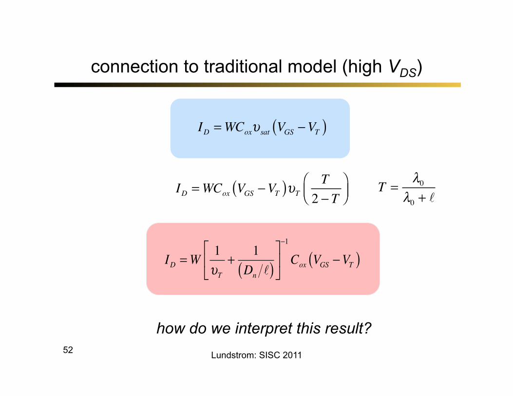
connection to traditional model (high VDS)
how do we interpret this result?
ID =WCox VGS −VT( )υTT2 − T
⎛⎝⎜
⎞⎠⎟
ID =W1υT
+1
Dn ( )⎡
⎣⎢
⎤
⎦⎥
−1
Cox VGS −VT( )
ID =WCoxυsat VGS −VT( )
Lundstrom: SISC 2011
T =λ0
λ0 +
53
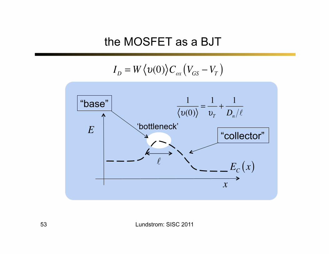
the MOSFET as a BJT
ID =W υ(0) Cox VGS −VT( )
EC x( )x
E
1υ(0)
=1υT
+1
Dn
‘bottleneck’ “collector”
“base”
Lundstrom: SISC 2011
54
outline
Lundstrom: SISC 2011
1) Introduction 2) Traditional Approach 3) MOS electrostatics 4) The ballistic MOSFET 5) Comparison to experiments 6) Scattering in nano-MOSFETs 7) MOSFETs below 10 nm 8) Summary
55
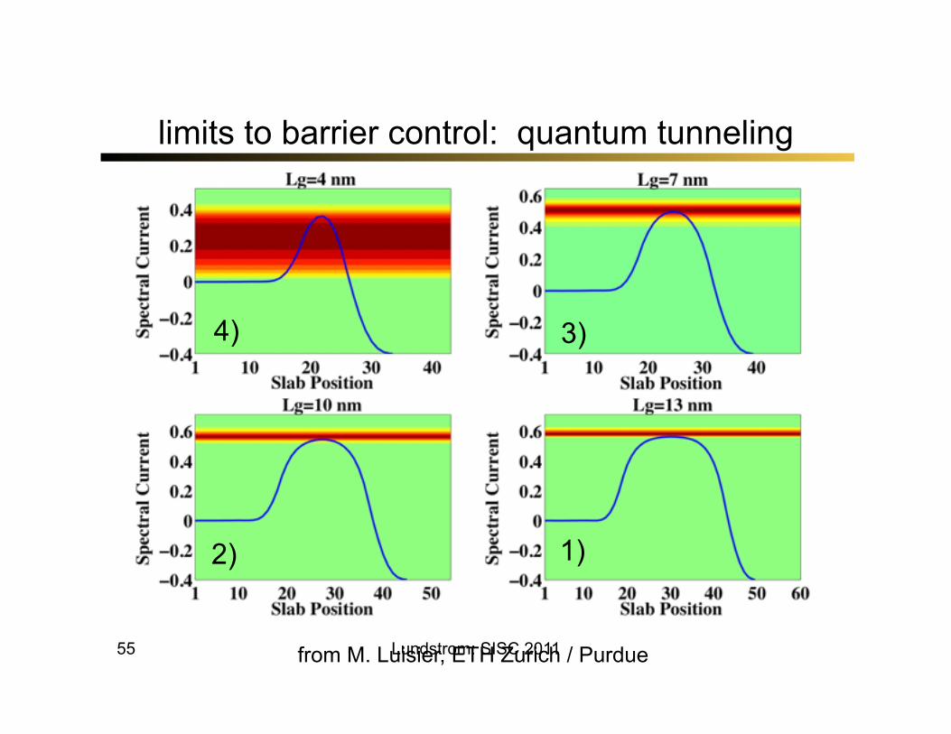
limits to barrier control: quantum tunneling
from M. Luisier, ETH Zurich / Purdue
4) 3)
2) 1)
Lundstrom: SISC 2011
56
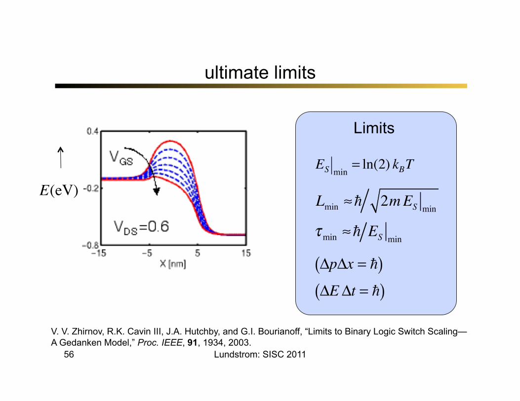
ultimate limits
Lundstrom: SISC 2011
V. V. Zhirnov, R.K. Cavin III, J.A. Hutchby, and G.I. Bourianoff, “Limits to Binary Logic Switch Scaling—A Gedanken Model,” Proc. IEEE, 91, 1934, 2003.
�
ES min = ln(2) kBT
Lmin ≈ 2mES min
τmin ≈ ES min
Limits
�
ΔpΔx = ( )
�
ΔEΔt = ( )
E(eV)
57
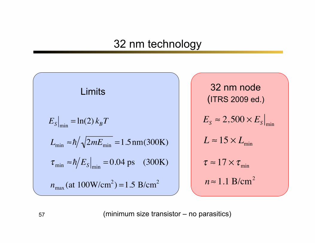
32 nm technology
�
ES min = ln(2) kBT
�
Lmin ≈ 2mEmin =1.5nm(300K)
�
τmin ≈ ES min = 0.04 ps (300K)
Limits
�
nmax (at 100W/cm2) =1.5 B/cm2
32 nm node (ITRS 2009 ed.)
ES ≈ 2,500 × ES min
L ≈ 15 × Lmin
τ ≈ 17 × τmin
n≈ 1.1 B/cm2
(minimum size transistor – no parasitics)
58
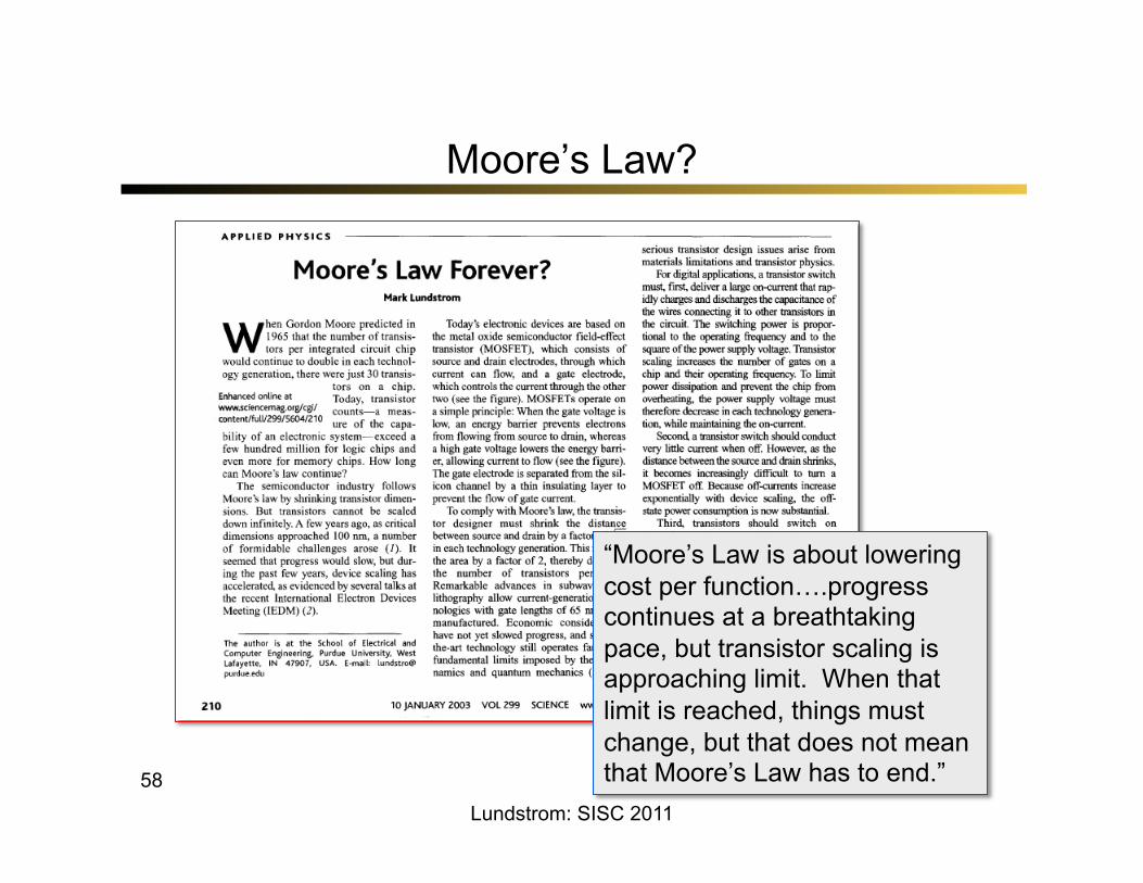
Moore’s Law?
“Moore’s Law is about lowering cost per function….progress continues at a breathtaking pace, but transistor scaling is approaching limit. When that limit is reached, things must change, but that does not mean that Moore’s Law has to end.”
Lundstrom: SISC 2011
59
outline
Lundstrom: SISC 2011
1) Introduction 2) Traditional Approach 3) MOS electrostatics 4) The ballistic MOSFET 5) Comparison to experiments 6) Scattering in nano-MOSFETs 7) MOSFETs below 10nm 8) Summary
60
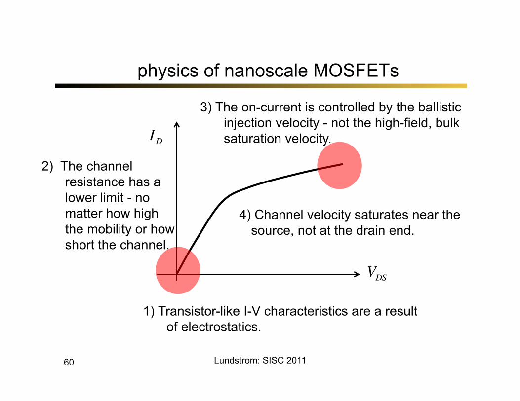
physics of nanoscale MOSFETs
VDS
ID
1) Transistor-like I-V characteristics are a result of electrostatics.
2) The channel resistance has a lower limit - no matter how high the mobility or how short the channel.
3) The on-current is controlled by the ballistic injection velocity - not the high-field, bulk saturation velocity.
4) Channel velocity saturates near the source, not at the drain end.
Lundstrom: SISC 2011
61
limits of scaling
Lundstrom: SISC 2011
What happens below 10 nm?
62
for more information
Lundstrom: SISC 2011
1) “Physics of Nanoscale MOSFETs,” a series of eight lectures on the subject presented at the 2008 NCN@Purdue Summer School by Mark Lundstrom, 2008.
http://nanohub.org/resources/5306
2) “Electronic Transport in Semiconductors,” Lectures 1-8, by Mark Lundstrom, 2011. http://nanohub.org/resources/11872
4) “Lessons from Nanoscience,” http://nanohub.org/topics/LessonsfromNanoscience
3) “Electronics from the Bottom Up” http://nanohub.org/topics/ElectronicsFromTheBottomUp
nanoHUB-U
63 Lundstrom: SISC 2011
http://nanoHUB.org/u
64
Thank you!
Lundstrom: SISC 2011
1) Introduction 2) Traditional Approach 3) MOS electrostatics 4) The ballistic MOSFET 5) Comparison to experiments 6) Scattering in nano-MOSFETs 7) MOSFETs below 10nm 8) Summary