M. REICHEN et al., Characterisation of an Adhesive-free Packaging System for…, Chem. Biochem. Eng. Q., 28 (2) 189–202 (2014) 189 Introduction The development of microfluidic devices is an iterative process that involves series of improve- ments in performance, functionality, or reproduc- ibility before arriving at the final design. Analogous to a programming language, a distinction between high-level and low-level functions can be made. In this distinction, high-level functions (HLF) relate to the ultimate application, whilst the low-level func- tions (LLF) refer to the more basic operational re- quirements, such as packaging, fluidic connections, or electrical and optical connections, which may be needed for the integration of sensors and actuators. Typically, the LLF requirements are not addressed as transferable technical solutions, but often remain part of the overall iterative development process (Fig. 1). These LLFs can however become a major bottleneck in the design process, if they have to be addressed with each iteration. Accordingly, an ap- proach that allows researchers to concentrate their efforts on meeting the requirements for the HLFs (whilst keeping the efforts for the LLFs to a mini- mum), would streamline the design process. One plausible solution is found in the modular assembly of pre-fabricated chip components as pre- sented in studies of rapid prototyping in microfluid- ics. 1,2 By decoupling the chip development from the packaging, the modular approach facilitates trans- ferable technologies addressing LLFs such as seal- ing, assembly, accessibility and connectivity with auxiliary components. Furthermore, modularity opens up the opportunity to standardise components for LLFs. Design considerations particular to the devel- opment of microfluidic biochemical reactors pose additional demands. For successful operation, both small and comparatively large features need to be integrated on the same chip. 3–5 Specifically, cham- bers for the culture of cells, with volumes of tens to hundreds of microliters, need to connect with low volume microfluidic channels that provide the nec- essary culture components. Additionally, biochemi- cal reactors typically necessitate use of polymeric materials. These facilitate integration with optical detection methods, which have found widespread use for the monitoring of reaction or culture condi- Characterisation of an Adhesive-free Packaging System for Polymeric Microfluidic Biochemical Devices and Reactors M. Reichen, A. Super, M. J. Davies, R. J. Macown, B. O’Sullivan, T. V. Kirk, M. P. C. Marques, N. Dimov, and N. Szita * Department of Biochemical Engineering, University College London, Torrington Place, London, WC1E 7JE, UK The development of microfluidic devices is an iterative process that involves series of improvements, which can be costly and time consuming. We present a packaging sys- tem which makes use of an accessible rapid prototyping method, and facilitates the rapid and reliable implementation of polymeric microfluidic device designs. The packaging system uses a modular design and is based on an adhesive-free connection of a reusable and stiff polymeric interface plate with a disposable, soft microfluidic chip under com- pression. We characterised the system by numerically and experimentally studying the effect of compression and key dimensions on burst pressure and flow rate. All parts are fabricated with readily available low-cost materials and micro-milling technology. The presented approach is both facilitating and systematising the fabrication of devices with different degrees of complexity; keeping assembly and interconnection simple and straightforward. Furthermore, minimising the time between a design and a finished working prototype yields rapid verification of microfluidic design concepts and testing of assays. Several chip designs were fabricated, then growth of stem cells and hydrodynam- ic vertical flow focusing in a microfluidic device were realised using our approach. Our approach minimises the need for re-development and re-testing of interface components; reducing cost and time requirements. Key words: packaging, rapid prototyping, micro milling, micro reactors, stem cell culture, hydro- dynamic vertical flow focussing doi: 10.15255/CABEQ.2014.1937 Original scientific paper Received: January 13, 2014 Accepted: April 2, 2014 * Corresponding author: Nicolas Szita, tel: +44 207 679 4418, e-mail: [email protected]
Transcript
M. REICHEN et al., Characterisation of an Adhesive-free Packaging System for…, Chem. Biochem. Eng. Q., 28 (2) 189–202 (2014) 189
Introduction
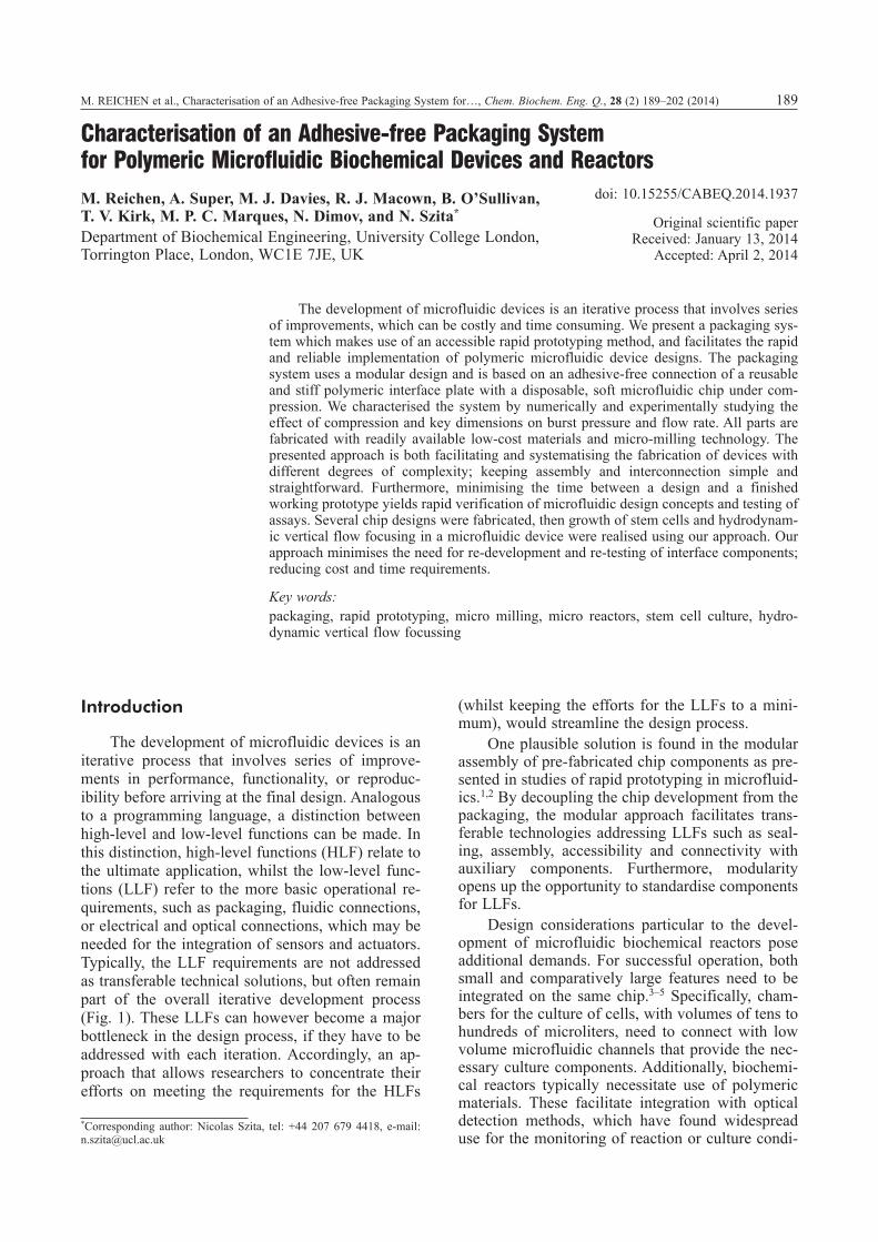
The development of microfluidic devices is an iterative process that involves series of improve-ments in performance, functionality, or reproduc-ibility before arriving at the final design. Analogous to a programming language, a distinction between high-level and low-level functions can be made. In this distinction, high-level functions (HLF) relate to the ultimate application, whilst the low-level func-tions (LLF) refer to the more basic operational re-quirements, such as packaging, fluidic connections, or electrical and optical connections, which may be needed for the integration of sensors and actuators. Typically, the LLF requirements are not addressed as transferable technical solutions, but often remain part of the overall iterative development process (Fig. 1). These LLFs can however become a major bottleneck in the design process, if they have to be addressed with each iteration. Accordingly, an ap-proach that allows researchers to concentrate their efforts on meeting the requirements for the HLFs
(whilst keeping the efforts for the LLFs to a mini-mum), would streamline the design process.
One plausible solution is found in the modular assembly of pre-fabricated chip components as pre-sented in studies of rapid prototyping in microfluid-ics.1,2 By decoupling the chip development from the packaging, the modular approach facilitates trans-ferable technologies addressing LLFs such as seal-ing, assembly, accessibility and connectivity with auxiliary components. Furthermore, modularity opens up the opportunity to standardise components for LLFs.
Design considerations particular to the devel-opment of microfluidic biochemical reactors pose additional demands. For successful operation, both small and comparatively large features need to be integrated on the same chip.3–5 Specifically, cham-bers for the culture of cells, with volumes of tens to hundreds of microliters, need to connect with low volume microfluidic channels that provide the nec-essary culture components. Additionally, biochemi-cal reactors typically necessitate use of polymeric materials. These facilitate integration with optical detection methods, which have found widespread use for the monitoring of reaction or culture condi-
Characterisation of an Adhesive-free Packaging System for Polymeric Microfluidic Biochemical Devices and Reactors
M. Reichen, A. Super, M. J. Davies, R. J. Macown, B. O’Sullivan, T. V. Kirk, M. P. C. Marques, N. Dimov, and N. Szita*
Department of Biochemical Engineering, University College London, Torrington Place, London, WC1E 7JE, UK
The development of microfluidic devices is an iterative process that involves series of improvements, which can be costly and time consuming. We present a packaging sys-tem which makes use of an accessible rapid prototyping method, and facilitates the rapid and reliable implementation of polymeric microfluidic device designs. The packaging system uses a modular design and is based on an adhesive-free connection of a reusable and stiff polymeric interface plate with a disposable, soft microfluidic chip under com-pression. We characterised the system by numerically and experimentally studying the effect of compression and key dimensions on burst pressure and flow rate. All parts are fabricated with readily available low-cost materials and micro-milling technology. The presented approach is both facilitating and systematising the fabrication of devices with different degrees of complexity; keeping assembly and interconnection simple and straightforward. Furthermore, minimising the time between a design and a finished working prototype yields rapid verification of microfluidic design concepts and testing of assays. Several chip designs were fabricated, then growth of stem cells and hydrodynam-ic vertical flow focusing in a microfluidic device were realised using our approach. Our approach minimises the need for re-development and re-testing of interface components; reducing cost and time requirements.
190 M. REICHEN et al., Characterisation of an Adhesive-free Packaging System for…, Chem. Biochem. Eng. Q., 28 (2) 189–202 (2014)
tions. Furthermore, they can enable the fabrication of disposable devices, which facilitate the required sterilisation procedures.
Direct writing methods, such as CO2 laser writ-ing,6 offer rapid fabrication of polymeric chips with feature sizes of ~100 µm (larger feature sizes can be obtained by writing several adjacent ‘passes’). However, reproducing the chip (to make the chip disposable or generate multiple units) can introduce unnecessary variations in dimensional fidelity and back end processing. In contrast, fabrication of mul-tiple prototype chips by casting and moulding from a master greatly reduces dimensional variations (be-tween devices) and the preparation time of individ-ual chips.7,8 Low aspect ratio features can be easily produced via soft lithography techniques,9–12 how-ever, they require clean room access which can be costly.13 Micro milling, or precision milling,14,15 ap-proaches are appealing for the fabrication of bio-chemical microdevices; micro milling offers a low budget and robust approach for the micromachining of moulds with different feature sizes, and its ma-chinery is typically more accessible.
For most applications, microfluidic devices re-quire several pieces of peripheral equipment. There-fore, connections to the macro-world, such as pumps, actuators, waveguides and electrodes, need to be provided in the form of reliable and reproduc-ible technical solutions.16 A wide range of intercon-nects, such as those reviewed by Fredrickson and Fan,17 have been presented. These can be broadly divided into two classes, permanent and non-perma-nent interconnects. Permanent connections typically rely on adhesives, often epoxy resins, to attach tub-ing to the microfluidic chip either directly or via commercially available connection ports such as the NanoPort™ assembly. This approach requires an operator to repeat the interconnection attachment process for each test chip, and reproducibility may
depend on their dexterity.18–20 There is also an asso-ciated risk of the adhesive entering the microfluidic channels and connections, which may not be com-patible with the envisaged assay;21 biocompatibility being crucial for life sciences applications.
Non-permanent interconnect solutions have the advantage of being reusable – an important consid-eration if multiple prototypes need to be tested rap-idly. Forming a reliable seal however requires a more complex design than permanent systems; O-ring or custom gasket systems,22–25 press-fit de-signs26–29 and magnetic clamps30 have been de-scribed. Non-permanent interconnects can be inte-grated into chip fabrication19,31 or can be decoupled entirely from the chip.21 Decoupling may be pre-ferred as it allows simplified chip fabrication and reuse of the same interconnects for multiple experi-ments, reducing variability; and – as mentioned be-fore – modular approaches facilitate standardisa-tion.
The aim of this study is to present and charac-terise a packaging system and prototyping method for the fabrication of polymeric microfluidic bio-chemical devices. The method uses a disposable sil-icone microfluidic chip, and a modular, reusable, non-integrated, adhesive-free, and self-aligning in-terconnect and packaging system. Care has been given to standardisation: chip dimensions are com-patible with common microscope slides, all device components and mould masters were fabricated with a low-cost, readily available micro-milling ma-chine, and fluidic connectors are based on widely accessible M6 fittings. Basic design rules (e.g. mi-crochannel dimensions) have been extracted from finite element method simulations. The presented packaging and rapid prototyping of the poly(di-methylsiloxane) (PDMS) chips offers a simple but comprehensive route for the production of micro-
F i g . 1 – Design process. Iterations for design improvement are expected (solid line) and undesired for device reliability (dashed line). The desired and expected iterations include a short phase of virtual prototyping, i.e. the use of design and modelling software to check the performance of the design idea. This is then ideally followed by a rapid translation of the design to a sufficient number of working prototypes for rapid performance and reliability verification. Undesired iterations, caused for example by deficiencies in the interconnect (IC) or by poor bonding (B), unnecessarily delay this translation to working prototypes and necessitate effort and time that could otherwise be employed to further improve the design for the desired application.
M. REICHEN et al., Characterisation of an Adhesive-free Packaging System for…, Chem. Biochem. Eng. Q., 28 (2) 189–202 (2014) 191
fluidic devices for biochemical applications with minimal equipment and no cleanroom facilities.
Several proof-of-concept experiments were conducted to validate the proposed framework. Firstly, three various two-input mixing devices were fabricated to demonstrate integration of multiple in-terconnect ports in the packaging system. Secondly, two different cell culture PDMS chips were fabri-cated from precision milled aluminium moulds to demonstrate biological relevance. Additionally, per-fusion culture of human embryonic stem cell colo-nies32 was demonstrated. Finally, a hydrodynamic vertical flow-focusing device showed the compati-bility of our packaging approach with multilayer structures comprised of thin slabs of cast PDMS.
Materials and methods
Fabrication of the modular interconnect, the packaging system and the moulds
All machined parts were designed with a 3-D CAD program (SolidWorks, Dassault Systems, France) and CNC-code was generated with a CAM program (Mastercam X2, Mastercam, USA). A mi-cro-milling machine (M3400E, Folken Industries, USA) with a standard length, 2 flute, 2 mm diame-ter end mill (Kyocera Micro Tools, USA) was used to manufacture all parts of the packaging system. For the moulds 2-flute end mills of different diame-ters were employed (Kyocera Micro Tools, USA, and Performance Micro Tools, USA).
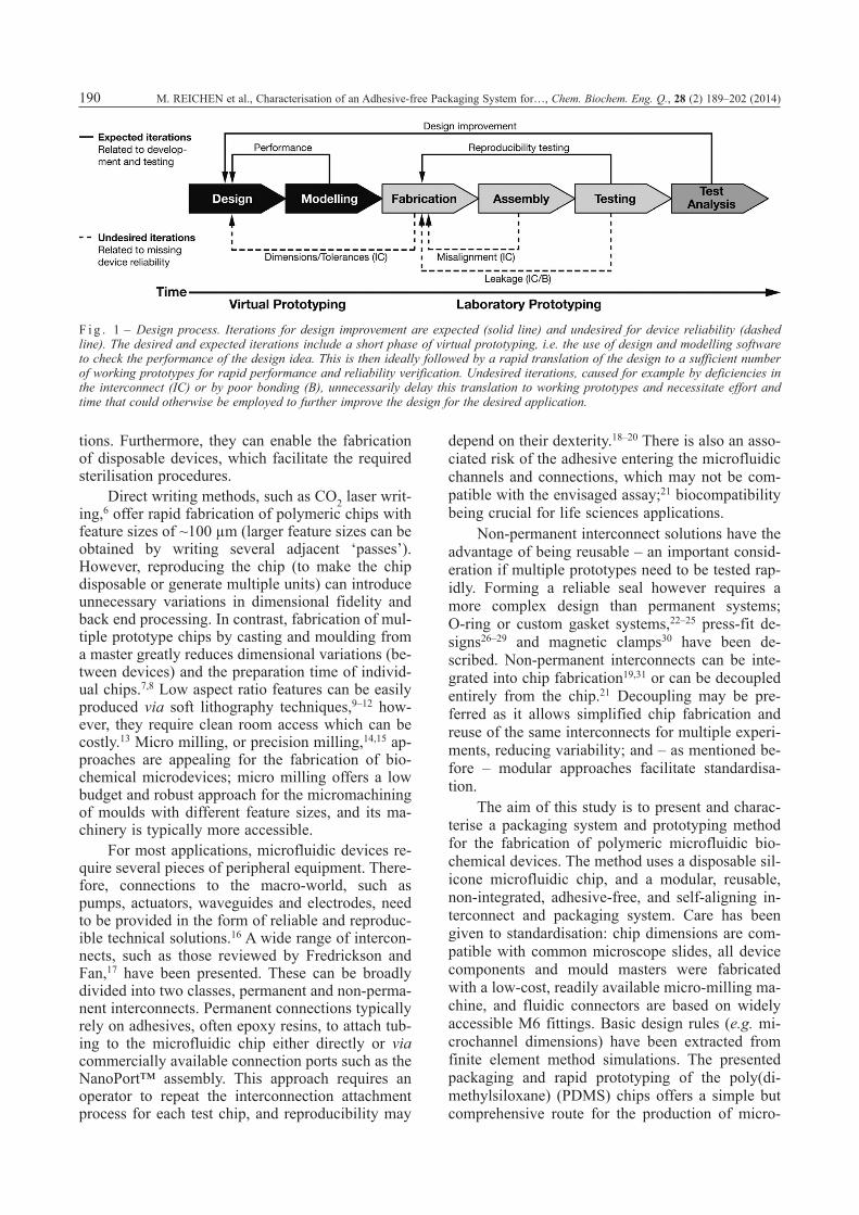
The interface plate and the socket for the fit-tings were milled from 5 mm thick polymer (Fig. 2(a)). M3 and M6 threads were manually cut in the appropriate bores for attachment of the sockets, and for the fittings in the sockets, respectively. Devices for cell culture and hydrodynamic cell focusing uti-lised polycarbonate to facilitate autoclave sterilisa-tion while earlier devices for 2-input mixing and burst pressure measurements made use of poly(meth-ylmethacrylate) (PMMA) (note that other hard polymers can be substituted if desired). The frame and the moulds were milled from 3 mm thick alu-minium sheets. M3 threads for the screws to hold the interface plate in place were manually cut in the appropriate bores in the aluminium frame.
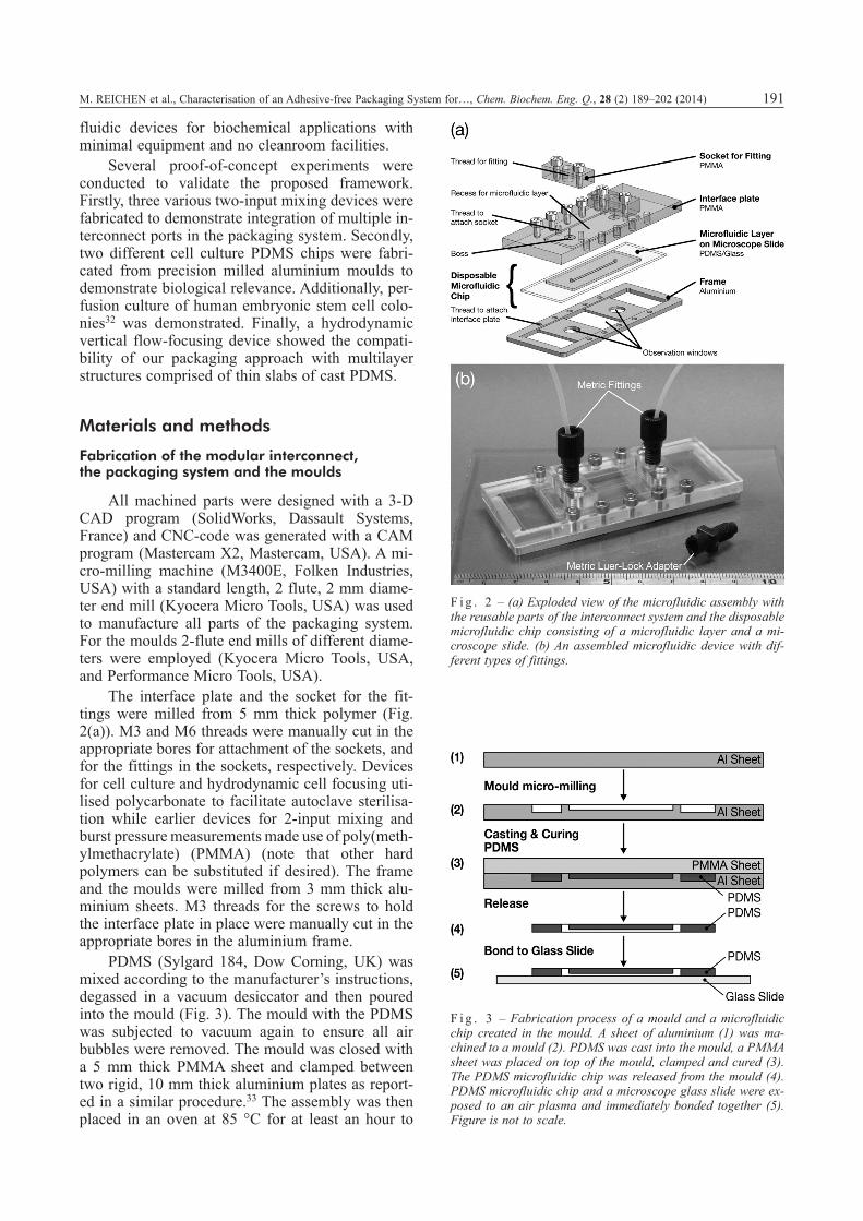
PDMS (Sylgard 184, Dow Corning, UK) was mixed according to the manufacturer’s instructions, degassed in a vacuum desiccator and then poured into the mould (Fig. 3). The mould with the PDMS was subjected to vacuum again to ensure all air bubbles were removed. The mould was closed with a 5 mm thick PMMA sheet and clamped between two rigid, 10 mm thick aluminium plates as report-ed in a similar procedure.33 The assembly was then placed in an oven at 85 °C for at least an hour to
F i g . 2 – (a) Exploded view of the microfluidic assembly with the reusable parts of the interconnect system and the disposable microfluidic chip consisting of a microfluidic layer and a mi-croscope slide. (b) An assembled microfluidic device with dif-ferent types of fittings.
F i g . 3 – Fabrication process of a mould and a microfluidic chip created in the mould. A sheet of aluminium (1) was ma-chined to a mould (2). PDMS was cast into the mould, a PMMA sheet was placed on top of the mould, clamped and cured (3). The PDMS microfluidic chip was released from the mould (4). PDMS microfluidic chip and a microscope glass slide were ex-posed to an air plasma and immediately bonded together (5). Figure is not to scale.
192 M. REICHEN et al., Characterisation of an Adhesive-free Packaging System for…, Chem. Biochem. Eng. Q., 28 (2) 189–202 (2014)
cure the PDMS. After curing, the clamp was dis-mantled and the PDMS microfluidic layer released with tweezers. To seal the disposable microfluidic layer, a microscope glass slide was bonded to the PDMS microfluidic layer using air plasma. Both parts were thoroughly cleaned with deionised water and ethanol and dried prior to bonding. To align the microfluidic layer with the microscope glass slide, the glass slide was placed in the frame and the mi-crofluidic layer in the recess of the interface plate. The two surfaces to be bonded were placed in a plasma chamber (90 s, 30 W, 500 mTorr, PDC-002, Harrick Plasma, USA). The interface plate and frame were aligned and pressed together gently, en-suring that the PDMS and glass components of the chip were correctly placed. The microfluidic chip was then removed from the frame, and cured in an oven at 85 ºC for at least 2 hours.
Characterisation of the fabrication method
The height of a microchannel feature in an alu-minium mould, the depth of the corresponding fea-ture in a PDMS cast, and the surface roughness Ra
were measured with a stylus profiler (Dektak 8, Veeco, USA). The stylus force was chosen to be 10 mg and the scan length was 2 mm. To measure the height of the protruding boss, a standard microme-ter calliper was used. A compact digital microscope (AM413T, Dino-Lite, USA) was used for imaging the different bosses, and the diameters measured us-ing image analysis software (ImageJ, NIH, USA). Boss geometries in an interface plate were mea-sured six times and the mean and standard deviation calculated.
Experimental setup for burst pressure measurement
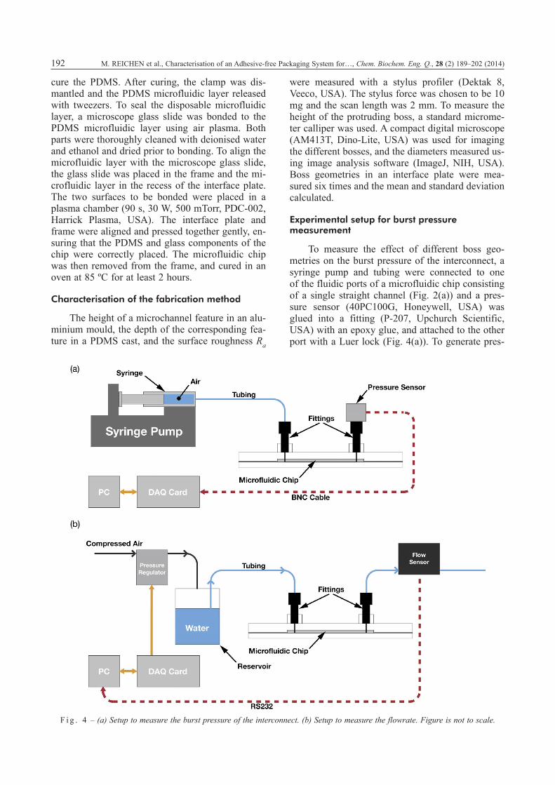
To measure the effect of different boss geo-metries on the burst pressure of the interconnect, a syringe pump and tubing were connected to one of the fluidic ports of a microfluidic chip consisting of a single straight channel (Fig. 2(a)) and a pres-sure sensor (40PC100G, Honeywell, USA) was glued into a fitting (P-207, Upchurch Scientific, USA) with an epoxy glue, and attached to the other port with a Luer lock (Fig. 4(a)). To generate pres-
F i g . 4 – (a) Setup to measure the burst pressure of the interconnect. (b) Setup to measure the flowrate. Figure is not to scale.
M. REICHEN et al., Characterisation of an Adhesive-free Packaging System for…, Chem. Biochem. Eng. Q., 28 (2) 189–202 (2014) 193
sure, a syringe pump was used to push air into the chip from a 5 mL syringe with a Luer lock connec-tor.
The force applied to the interface plate was controlled by tightening the screws to torques rang-ing from 2 N cm to 5 N cm using a torque screw driver. A LabVIEW™ routine (LabVIEW 8.2, Na-tional Instruments, USA) was used to log the pres-sure readings from a data acquisition card (USB-6229BNC, National Instruments, USA). The burst pressure was taken as the highest recorded applied pressure for a given experiment, and was measured six times for each torque setting.
Experimental setup for flow rate characterisation
With a soft elastomeric material such as PDMS some degree of channel deformation is to be ex-pected, whether from compression by a clamping procedure, or from the hydrostatic pressure within the channel required for flow.34 To characterise the flow rate, a pressurised reservoir of water was used to deliver a constant flow rate, which was moni-tored by a flowmeter (Fig. 4(b)). The setup consist-ed of a pressure regulator (ITV0011-2BL-Q, SMC, UK), a fluid reservoir, a single channel microfluidic chip (Fig. 2(a)) and a flowmeter (SLG1430-480, Sensirion, Switzerland). The fluid reservoir had two custom-made ports built into the lid to connect to the pressure regulator and to the microfluidic chip, respectively. A Luer lock fitting was used to con-nect the reservoir with polyvinyl chloride tubing to the pressure regulator, which was connected to a compressed air supply. The other port had an M6 thread to accommodate a threaded flat bottom fit-ting. A fitting was attached to a 15 cm length of PTFE tubing with the same fitting at the other end to connect to the microfluidic chip. The microfluid-ic chip was fitted on the other fluidic port with a male Luer-lock adapter. A 5 cm long PTFE tubing was fitted on one end with an M6 fitting and a fe-male Luer-lock adapter to connect to the microflu-idic chip and on the other end with an adapter to connect to the flow meter. The adapter was fitted with a 300 µm inner diameter capillary, which was cut to a length of 5 cm. Flow rates were recorded over 15 minutes, and the mean and standard devia-tion calculated.
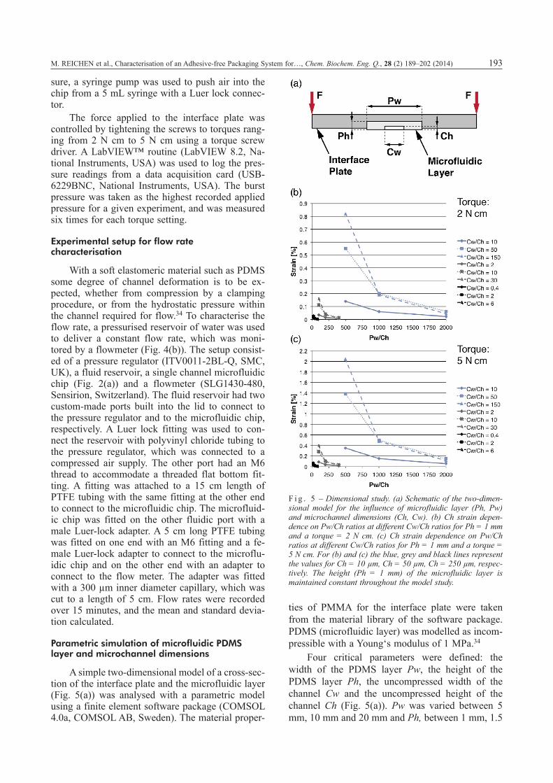
Parametric simulation of microfluidic PDMS layer and microchannel dimensions
A simple two-dimensional model of a cross-sec-tion of the interface plate and the microfluidic layer (Fig. 5(a)) was analysed with a parametric model using a finite element software package (COMSOL 4.0a, COMSOL AB, Sweden). The material proper-
ties of PMMA for the interface plate were taken from the material library of the software package. PDMS (microfluidic layer) was modelled as incom-pressible with a Young‘s modulus of 1 MPa.34
Four critical parameters were defined: the width of the PDMS layer Pw, the height of the PDMS layer Ph, the uncompressed width of the channel Cw and the uncompressed height of the channel Ch (Fig. 5(a)). Pw was varied between 5 mm, 10 mm and 20 mm and Ph, between 1 mm, 1.5
F i g . 5 – Dimensional study. (a) Schematic of the two-dimen-sional model for the influence of microfluidic layer (Ph, Pw) and microchannel dimensions (Ch, Cw). (b) Ch strain depen-dence on Pw/Ch ratios at different Cw/Ch ratios for Ph = 1 mm and a torque = 2 N cm. (c) Ch strain dependence on Pw/Ch ratios at different Cw/Ch ratios for Ph = 1 mm and a torque = 5 N cm. For (b) and (c) the blue, grey and black lines represent the values for Ch = 10 µm, Ch = 50 µm, Ch = 250 µm, respec-tively. The height (Ph = 1 mm) of the microfluidic layer is maintained constant throughout the model study.
194 M. REICHEN et al., Characterisation of an Adhesive-free Packaging System for…, Chem. Biochem. Eng. Q., 28 (2) 189–202 (2014)
mm and 2 mm. Values for Ch were varied between 10 µm, 50 µm and 250 µm and for Cw, between 100 µm, 500 µm and 1.5 mm.
The glass slide sealing the PDMS microchan-nel was assumed to be rigid, therefore imposing a zero-displacement boundary condition at the inter-face microfluidic layer/microscope glass slide. The torque applied to a screw results in an axial force on the interface plate, and point loads at the edges of the plate were used to represent this force generated by the screws. Friction losses between screw head and interface plate were neglected. The strain of the channel was calculated for the middle of the chan-nel roof by dividing the displacement at this point by the nominal height.
Hydrodynamic vertical flow focussing
Experiments were performed using a water blue dye (Sigma Adrich, UK) dissolved in reverse osmosis (RO) water as the focussed fluid and RO water as the sheath fluid. Bubble-free fluidic prim-ing of the device was completed by pumping 70 % ethanol solution into both inputs. The dye solution and sheath fluid were pumped into the hydrody-namic vertical flow focussing (HFF) device via sep-arate syringe pumps (Model 200, KD Scientific, USA) with a combined total flow rate of 200 µL min–1. Transmission of light from an LED (L600-01V, Epitex, Japan) passing through the main fluid channel was measured using a photodetector (PDA36A, Thorlabs, USA). A function generator (FG100, Grundig Intermedia GmbH, Germany) provided a square wave signal oscillating at a fre-quency of 2 kHz to the LED. Both the voltage from the photodetector and a reference signal from the function generator were fed into a lock-in amplifier (SR830, Stanford Research Systems, USA) to de-tect signal amplitude. Analysis of the text file out-put by the LabVIEW™ virtual instrument (vi) was performed in MATLAB (MathWorks, USA).
Human embryonic stem cell cultivation
Co-culture of human embryonic stem cells on inactivated mouse embryonic fibroblasts was car-ried out as previously described.32 Briefly, reusable components and the PDMS chip were sterilised sep-arately by autoclave before assembly in a biological safety cabinet. Culture surface coating and cell seeding were carried out by pipette before placing the system in an incubator during cell attachment. The culture chamber was then sealed with a reseal-able lid and culture media perfused by syringe pump for 2 days.
Results and discussion
Design and concept of the modular interconnect and packaging system
In the system presented here, the implementa-tion of a standard microscope slide format (3 x 1 inches) for the rigid part of the chip allows the use of different commercially available materials, such as tissue culture polystyrene (TC-PS). This is par-ticularly useful for microfluidic devices for cell cul-ture where a growth substrate consisting of TC-PS is desirable.35 The compatibility with this slide for-mat also facilitates the integration of microfluidic chips with routine end-point analyses that operate with standard microscope slides. For observation during the experiment, the centre opening in the bottom frame allows positioning of the objective of an inverted microscope in close proximity to the slide. Further observation windows under the sock-ets enable visual detection of leaking fluidic con-nections that may result from faulty or poorly de-signed PDMS chips.
Tubing is reliably connected to the top plate us-ing designated socket modules. The socket modules are fixed with two screws to the interface plate, and automatically align with the inlet and outlet bores in the interface plate. Recesses in the interface plate enable self-alignment of the fluidic ports of the mi-crofluidic chip with the corresponding bores in the interface plate. A protruding boss machined into the recess seals the microfluidic chip with the packag-ing system (Fig. 6). This sealing concept decouples the sealing of the chip from the choice of the inter-connect type, and therefore provides flexibility in the choice of interconnects. The sockets can be used with different fitting types, for example standard adapters (Fig. 2(b)), or they can be modified for custom-made interconnects if required. Such sock-ets for screw type fittings have previously been used in combination with injection moulded cyclic olefin copolymer (COC) microfluidic devices,15 but this fabrication method is more amenable to mass fabrication than for rapid prototyping. In our sys-tem, due to its modularity, changes in the fitting/interconnect types or changes in the chip design can be made independently and do not require a rede-sign of the entire device.
Rapid prototyping fabrication and characterisation
To obtain a streamlined prototyping process, we investigated the use of a low-cost CNC mi-cro-milling machine towards the fabrication of both our packaging system and the moulds for microflu-idic chips. The milled moulds contained the struc-tures for the microfluidic channel and the fluidic
M. REICHEN et al., Characterisation of an Adhesive-free Packaging System for…, Chem. Biochem. Eng. Q., 28 (2) 189–202 (2014) 195
ports, and defined the standardised outer dimen-sions of the microfluidic layer. The microfluidic chips themselves were then obtained using standard casting and bonding methods (see section Fabrica-tion of the modular interconnect, the packaging sys-tem and the moulds for more details). Therefore, the entire development process did not require clean-room environments.
A number of different devices were fabricated using this integrated prototyping approach: (a) to characterise the packaging system and the quality of the aluminium moulds, and (b) to demonstrate that the proposed approach can be extended to more complex device designs. In general, for all devices, allowing 3–4 hours for milling, and 2 hours for each curing step, the development processes took less than two days. Feature sizes smaller than 50 µm, in the plane of the device, were achieved by this technique. Additionally, all materials were read-ily available at low cost.
For the characterisation of the packaging sys-tem (see sections Burst pressure measurement for burst pressure and Characterisation of flow rate for flow rate), devices with different boss dimensions
in the interface plate’s recess were fabricated. The dimensions of the boss were varied for the diameter D between 3 mm and 5.5 mm and for the height H between 75 µm and 125 µm (Fig. 6). For this char-acterisation, the microfluidic chips consisted of a single microchannel (nominal values: 200 µm in height, 1.25 mm in width and 36 mm in length) and two fluidic ports. The maximum difference between the nominal and measured boss heights was 10.7 % (Table 1). For all boss diameters, the maximum dif-ference between nominal and measured diameter was 2.9 % (Table 2).
Ta b l e 1 – Measurement of boss heights (n=6)
Nominal height (µm) Measured height ± std dev (µm)
75 67 ± 3
100 100 ± 9
125 118 ± 3
Ta b l e 2 – Measurement of boss diameters (n=6)
Nominal diameter (mm) Measured diameter ± std dev (mm)
3 3.02 ± 0.04
4 3.94 ± 0.02
5.5 5.66 ± 0.03
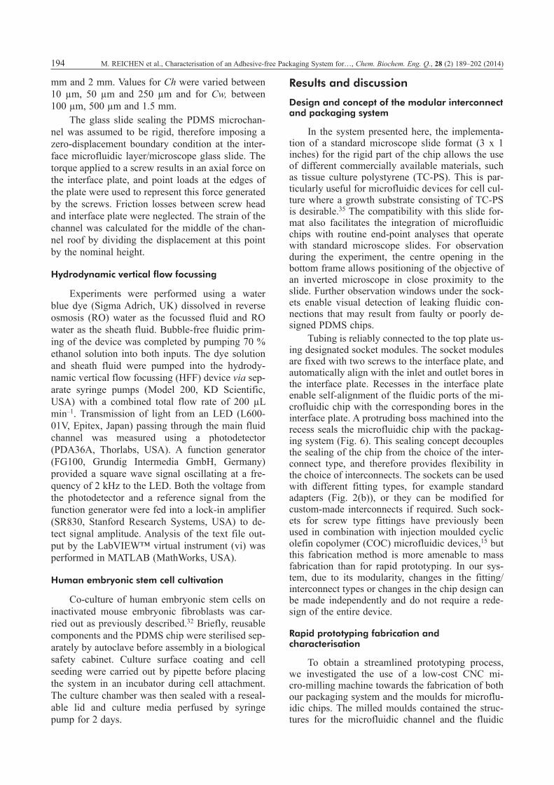
The microchannel feature height in the mould and the corresponding microchannel depth in the cast PDMS microfluidic layer were measured at three locations along the microchannel (Fig. 7(a)) using contact profilometry. The microchannel height in the mould had a mean of 188.5 µm, or a devia-tion of 5.8 %, of the nominal height and a standard deviation of 0.7 µm (Fig. 7(c)). The microchannel depth in the PDMS microfluidic layer had a mean of 185.4 µm, or a deviation of 7.3 %, of the nomi-nal depth and a standard deviation of 0.4 µm (Fig. 7(d)). The results show that a high fidelity be-tween the master and the moulded devices was achieved. Furthermore, the milled surfaces typically had Ra roughness measurements of approximately 180 nm, and are thus very smooth surfaces.
Before casting and curing of the microfluidic chips, no surface treatment of the mould was re-quired to prevent adhesion in the mould. The PDMS microfluidic layers from all mould geometries pre-sented were released easily and the moulds were reused. The subsequent plasma-assisted bonding of the PDMS microfluidic layer to a glass microscope slide was performed without any additional pro-cessing steps for the microfluidic layer (Fig. 7(b)).
F i g . 6 – Schematic of the interconnect, outlining crucial di-mensions of the boss (D, H) and recess (DR). The difference between the depth of the recess DR and the height of the micro-fluidic layer Ph limits the mechanical deformation of the micro-fluidic chip using the microscope slide as a bed stop. For this prototype, a maximum mechanical deformation of 100 µm has been allowed for the microfluidic chip. Therefore DR has been set at 0.9 mm, Ph at 1 mm. Figure is not to scale and the inter-face plate and the microfluidic layer are shown in exploded view to facilitate labelling of the dimensions.
196 M. REICHEN et al., Characterisation of an Adhesive-free Packaging System for…, Chem. Biochem. Eng. Q., 28 (2) 189–202 (2014)
Thus further demonstrating that the mould fabrica-tion method creates very smooth surfaces.
The quality of milled aluminium surfaces at-tained without polishing or other surface modifica-tions, combined with its durability and ease of cleaning after use, makes it a suitable material for mould fabrication. It is fabricated more rapidly than other monolithic masters such as micro-machined silicon masters or plastic masters made from sili-cone.36 Finally, the fabrication of microfluidic chips from moulds has advantages over directly milled parts. Namely, the minimum size of features (chan-nels, chambers etc) that can be directly milled is limited to the end mill (tool) diameter and length. Due to the inverse nature of moulds, smaller fea-tures may be achieved depending on the accuracy of the micro-milling machine, tool size, feature spacing, and material being milled. For example, it would be possible to mill around a single 200 μm wide, 1–2 mm tall ridge, and use this mould to cre-ate a channel of similar dimensions. Due to the high aspect ratio (i.e. the depth divided by the width), it would be very difficult to directly mill such a chan-nel with a standard tool; a typical tool with a diam-eter of 200 μm may have a maximum cutting depth of 600 μm.
In order to demonstrate that the rapid prototyp-ing method can easily be extended to more complex multilayer structures, a number of microfluidic demonstrators were prepared (Fig. 8). A three-di-mensional channel network (Fig. 8(a)), where co-loured liquid streams (blue and yellow food dyes in water) pass over and under each other before being combined, was fabricated by using two layers of PDMS and a system of through holes. The moulds were machined with a single 2 mm milling tool, us-ing PMMA rather than aluminium, demonstrating the versatility of materials that could be used with the mould fabrication technique. The alignment of the PDMS layers before bonding was achieved thanks to the standardisation of the outer dimen-sions. Feature sizes ranged from 125–1000 µm, much smaller than the 2 mm tool used to mill the mould. A functioning, leak-free prototype was suc-cessfully fabricated and tested within 24 hours of the final design being approved. Similarly, a stag-gered herringbone mixer, with grooves approxi-mately 35 µm wide (50 µm spaced grooves at a 45° angle), was prepared (using a 2 flute end mill with a 0.001 in. diameter), where a negative mould was machined from brass stock (Fig. 8(b)). Various y-channel mixing devices were fabricated to demon-strate integration of multiple interconnect ports in
F i g . 7 – (a) Schematic of the microfluidic layer and the indicated scan locations. (b) Assembled microfluidic layer on a microscope slide. (c, d) Height and depth profiles of the microfluidic layer in the mould and the PDMS microfluidic layer.
M. REICHEN et al., Characterisation of an Adhesive-free Packaging System for…, Chem. Biochem. Eng. Q., 28 (2) 189–202 (2014) 197
the packaging system (Fig. 8(c)). Finally, two cell culture chips fabricated from aluminium moulds are included to demonstrate biological applications (Fig. 8(d)). These chips are designed for eukaryote fermentation with active mixing and optical sensor integration37 and perfusion culture of human embry-onic stem cell colonies (discussed below as a case study, see Microfabricated device for adherent stem cell culture).
Numerical study of channel deformation of the microfluidic chip within the modular framework
Due to the nature of the presented packaging and LLF, a compression of the microfluidic layer occurs which affects the dimensions of the micro-fluidic structures that can affect the functionality of the device and the ultimate HLF. To study this de-formation, we analysed a simple two-dimensional finite element model of a cross-section of the inter-face plate with a microfluidic layer consisting of a single channel. To formulate design rules, a number of finite element calculations were performed for different geometries. The width of the PDMS, Pw,
and the uncompressed channel height, Ch, and width, Cw, were varied in a wide range. Fig. 5 ((b), (c)) shows the impact of the ratio of Pw:Ch on the strain of the channel height (percentage decrease in channel height) at mid-width of the channel at Ph = 1 mm. Strains are shown for different values of and Cw and Ch and for 2 N cm (b) and 5 N cm (c) of applied torque.
In general, for any given combination of Cw and Ch, the maximum strain occurs for low Pw/Ch ratios. A PDMS layer which is significantly wider than the microfluidic structures thus reduces the strain. This effect was observed for all values of Ph (data not shown). For Cw/Ch ratios below 10, strain in the channel is negligibly small for any channel height and torque setting. With the lowest channel height (10 μm) Cw/Ch ratios above 10 exhibit strains up to 1 % for 2 N cm torque, and up to 2.1 % strain for 5 N cm, respectively (Fig. 5(b), (c)). Hence, the width of the PDMS layer should be maximised and the ratio of channel width to chan-nel height kept below 10, particularly where low channel heights are desired. Increasing the height Ph decreases the strain on the microchannel (data
F i g . 8 – (a) A fluidic demonstrator showing some of the complexity that can be achieved with the rapid prototyping method. Coloured liquids flow through a three-dimensional channel network before combining. Dimensions: narrow channel, 200 µm (w) × 250 µm (h), wide channel, 1000 µm (w) × 125 µm (h). (b) Features as small as 35 µm can be fabricated, for example a mould with channel and a staggered herringbone mixer (Mixer structures are 20 µm deep, and 50 µm wide under a 45° angle. Dimensions of the microchannel: 200 µm (w) × 100 µm (h)). (c) Multiple ports can be realised, for example for mixer chips with different mixing lengths (d) The packaging and the fabrication method can also be used for chips for biological applications and integrated with optical sen-sors, for example suspension cultures or the culture of adherent cells such as embryonic stem cells.
198 M. REICHEN et al., Characterisation of an Adhesive-free Packaging System for…, Chem. Biochem. Eng. Q., 28 (2) 189–202 (2014)
not shown). A Ph of 1 mm however is a good com-promise which allows machining of the moulds in a reasonable time while microchannel strain can be maintained below 1 %.
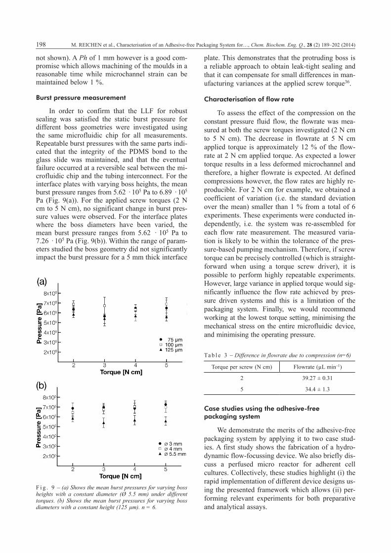
Burst pressure measurement
In order to confirm that the LLF for robust sealing was satisfied the static burst pressure for different boss geometries were investigated using the same microfluidic chip for all measurements. Repeatable burst pressures with the same parts indi-cated that the integrity of the PDMS bond to the glass slide was maintained, and that the eventual failure occurred at a reversible seal between the mi-crofluidic chip and the tubing interconnect. For the interface plates with varying boss heights, the mean burst pressure ranges from 5.62 · 105 Pa to 6.89 · 105 Pa (Fig. 9(a)). For the applied screw torques (2 N cm to 5 N cm), no significant change in burst pres-sure values were observed. For the interface plates where the boss diameters have been varied, the mean burst pressure ranges from 5.62 · 105 Pa to 7.26 · 105 Pa (Fig. 9(b)). Within the range of param-eters studied the boss geometry did not significantly impact the burst pressure for a 5 mm thick interface
plate. This demonstrates that the protruding boss is a reliable approach to obtain leak-tight sealing and that it can compensate for small differences in man-ufacturing variances at the applied screw torque36.
Characterisation of flow rate
To assess the effect of the compression on the constant pressure fluid flow, the flowrate was mea-sured at both the screw torques investigated (2 N cm to 5 N cm). The decrease in flowrate at 5 N cm applied torque is approximately 12 % of the flow-rate at 2 N cm applied torque. As expected a lower torque results in a less deformed microchannel and therefore, a higher flowrate is expected. At defined compressions however, the flow rates are highly re-producible. For 2 N cm for example, we obtained a coefficient of variation (i.e. the standard deviation over the mean) smaller than 1 % from a total of 6 experiments. These experiments were conducted in-dependently, i.e. the system was re-assembled for each flow rate measurement. The measured varia-tion is likely to be within the tolerance of the pres-sure-based pumping mechanism. Therefore, if screw torque can be precisely controlled (which is straight-forward when using a torque screw driver), it is possible to perform highly repeatable experiments. However, large variance in applied torque would sig-nificantly influence the flow rate achieved by pres-sure driven systems and this is a limitation of the packaging system. Finally, we would recommend working at the lowest torque setting, minimising the mechanical stress on the entire micro fluidic device, and minimising the operating pressure.
Ta b l e 3 – Difference in flowrate due to compression (n=6)
Torque per screw (N cm) Flowrate (µL min–1)
2 39.27 ± 0.31
5 34.4 ± 1.3
Case studies using the adhesive-free packaging system
We demonstrate the merits of the adhesive-free packaging system by applying it to two case stud-ies. A first study shows the fabrication of a hydro-dynamic flow-focussing device. We also briefly dis-cuss a perfused micro reactor for adherent cell cultures. Collectively, these studies highlight (i) the rapid implementation of different device designs us-ing the presented framework which allows (ii) per-forming relevant experiments for both preparative and analytical assays.
F i g . 9 – (a) Shows the mean burst pressures for varying boss heights with a constant diameter (Ø 5.5 mm) under different torques. (b) Shows the mean burst pressures for varying boss diameters with a constant height (125 µm). n = 6.
M. REICHEN et al., Characterisation of an Adhesive-free Packaging System for…, Chem. Biochem. Eng. Q., 28 (2) 189–202 (2014) 199
Hydrodynamic vertical flow focussing device for spectrophotometric uses
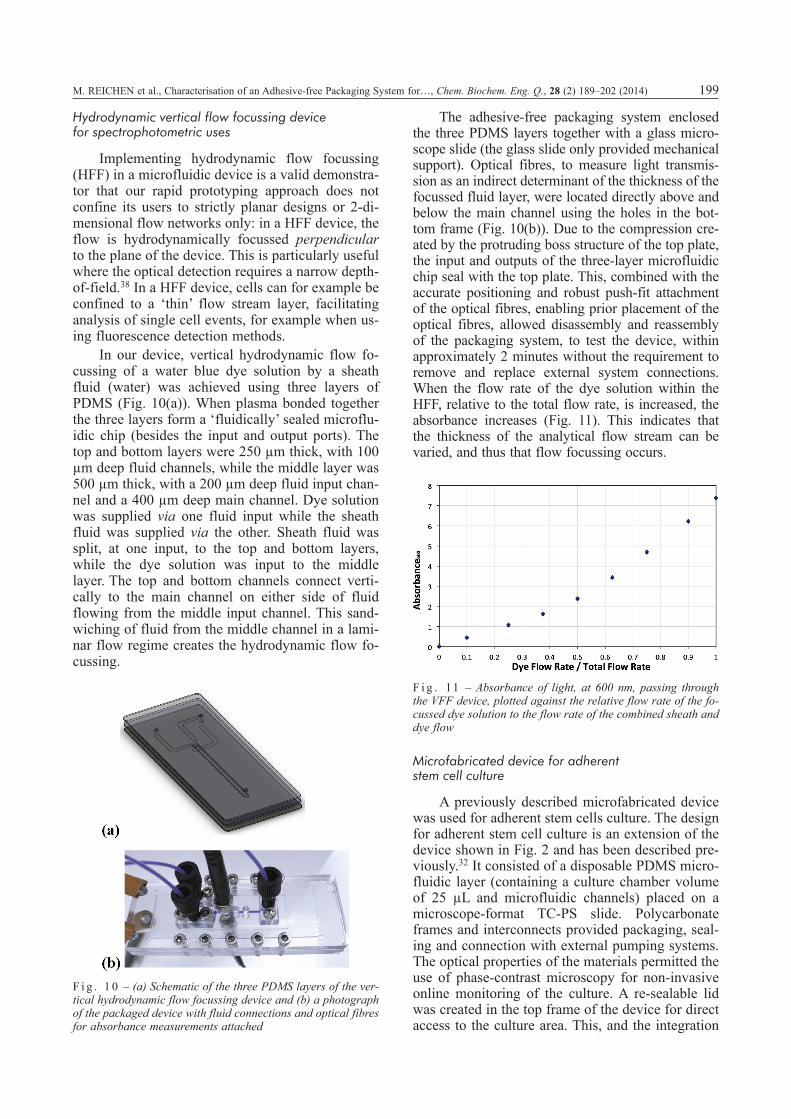
Implementing hydrodynamic flow focussing (HFF) in a microfluidic device is a valid demonstra-tor that our rapid prototyping approach does not confine its users to strictly planar designs or 2-di-mensional flow networks only: in a HFF device, the flow is hydrodynamically focussed perpendicular to the plane of the device. This is particularly useful where the optical detection requires a narrow depth-of-field.38 In a HFF device, cells can for example be confined to a ‘thin’ flow stream layer, facilitating analysis of single cell events, for example when us-ing fluorescence detection methods.
In our device, vertical hydrodynamic flow fo-cussing of a water blue dye solution by a sheath fluid (water) was achieved using three layers of PDMS (Fig. 10(a)). When plasma bonded together the three layers form a ‘fluidically’ sealed microflu-idic chip (besides the input and output ports). The top and bottom layers were 250 µm thick, with 100 µm deep fluid channels, while the middle layer was 500 µm thick, with a 200 µm deep fluid input chan-nel and a 400 µm deep main channel. Dye solution was supplied via one fluid input while the sheath fluid was supplied via the other. Sheath fluid was split, at one input, to the top and bottom layers, while the dye solution was input to the middle layer. The top and bottom channels connect verti-cally to the main channel on either side of fluid flowing from the middle input channel. This sand-wiching of fluid from the middle channel in a lami-nar flow regime creates the hydrodynamic flow fo-cussing.
The adhesive-free packaging system enclosed the three PDMS layers together with a glass micro-scope slide (the glass slide only provided mechanical support). Optical fibres, to measure light transmis-sion as an indirect determinant of the thickness of the focussed fluid layer, were located directly above and below the main channel using the holes in the bot-tom frame (Fig. 10(b)). Due to the compression cre-ated by the protruding boss structure of the top plate, the input and outputs of the three-layer microfluidic chip seal with the top plate. This, combined with the accurate positioning and robust push-fit attachment of the optical fibres, enabling prior placement of the optical fibres, allowed disassembly and reassembly of the packaging system, to test the device, within approximately 2 minutes without the requirement to remove and replace external system connections. When the flow rate of the dye solution within the HFF, relative to the total flow rate, is increased, the absorbance increases (Fig. 11). This indicates that the thickness of the analytical flow stream can be varied, and thus that flow focussing occurs.
Microfabricated device for adherent stem cell culture
A previously described microfabricated device was used for adherent stem cells culture. The design for adherent stem cell culture is an extension of the device shown in Fig. 2 and has been described pre-viously.32 It consisted of a disposable PDMS micro-fluidic layer (containing a culture chamber volume of 25 µL and microfluidic channels) placed on a microscope-format TC-PS slide. Polycarbonate frames and interconnects provided packaging, seal-ing and connection with external pumping systems. The optical properties of the materials permitted the use of phase-contrast microscopy for non-invasive online monitoring of the culture. A re-sealable lid was created in the top frame of the device for direct access to the culture area. This, and the integration
F i g . 1 0 – (a) Schematic of the three PDMS layers of the ver-tical hydrodynamic flow focussing device and (b) a photograph of the packaged device with fluid connections and optical fibres for absorbance measurements attached
F i g . 11 – Absorbance of light, at 600 nm, passing through the VFF device, plotted against the relative flow rate of the fo-cussed dye solution to the flow rate of the combined sheath and dye flow
200 M. REICHEN et al., Characterisation of an Adhesive-free Packaging System for…, Chem. Biochem. Eng. Q., 28 (2) 189–202 (2014)
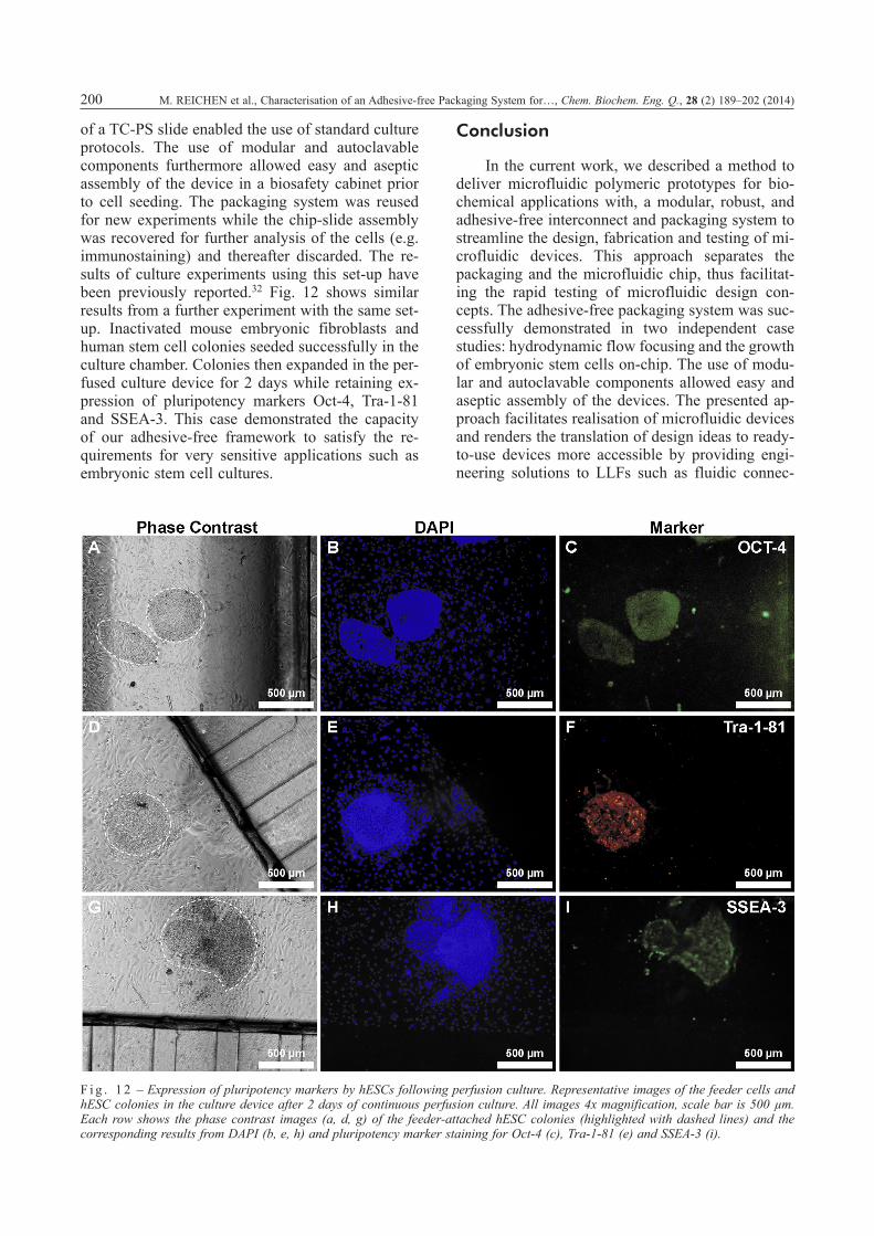
of a TC-PS slide enabled the use of standard culture protocols. The use of modular and autoclavable components furthermore allowed easy and aseptic assembly of the device in a biosafety cabinet prior to cell seeding. The packaging system was reused for new experiments while the chip-slide assembly was recovered for further analysis of the cells (e.g. immunostaining) and thereafter discarded. The re-sults of culture experiments using this set-up have been previously reported.32 Fig. 12 shows similar results from a further experiment with the same set-up. Inactivated mouse embryonic fibroblasts and human stem cell colonies seeded successfully in the culture chamber. Colonies then expanded in the per-fused culture device for 2 days while retaining ex-pression of pluripotency markers Oct-4, Tra-1-81 and SSEA-3. This case demonstrated the capacity of our adhesive-free framework to satisfy the re-quirements for very sensitive applications such as embryonic stem cell cultures.
Conclusion
In the current work, we described a method to deliver microfluidic polymeric prototypes for bio-chemical applications with, a modular, robust, and adhesive-free interconnect and packaging system to streamline the design, fabrication and testing of mi-crofluidic devices. This approach separates the packaging and the microfluidic chip, thus facilitat-ing the rapid testing of microfluidic design con-cepts. The adhesive-free packaging system was suc-cessfully demonstrated in two independent case studies: hydrodynamic flow focusing and the growth of embryonic stem cells on-chip. The use of modu-lar and autoclavable components allowed easy and aseptic assembly of the devices. The presented ap-proach facilitates realisation of microfluidic devices and renders the translation of design ideas to ready-to-use devices more accessible by providing engi-neering solutions to LLFs such as fluidic connec-
F i g . 1 2 – Expression of pluripotency markers by hESCs following perfusion culture. Representative images of the feeder cells and hESC colonies in the culture device after 2 days of continuous perfusion culture. All images 4x magnification, scale bar is 500 µm. Each row shows the phase contrast images (a, d, g) of the feeder-attached hESC colonies (highlighted with dashed lines) and the corresponding results from DAPI (b, e, h) and pluripotency marker staining for Oct-4 (c), Tra-1-81 (e) and SSEA-3 (i).
M. REICHEN et al., Characterisation of an Adhesive-free Packaging System for…, Chem. Biochem. Eng. Q., 28 (2) 189–202 (2014) 201
tions, establishing a template for chip designs, and avoiding the need for specialised environments such as cleanrooms. As part of our future work we are developing packaging systems that reduce the amount of screws necessary for the assembly of the devices.39
ACKNOWLEDGMENTS
The authors thank the staff at the London Cen-tre for Nanotechnology for their assistance with the Dektak measurements. We would like to thank the Engineering and Physical Sciences Research Coun-cil EPSRC (‘First Grant’, EP/I005471/1) and the Biotechnology and Biological Sciences Research Council BBSRC (BB/I00484X/1, BB/L000997/1) for funding. We also gratefully acknowledge the De-partment of Biochemical Engineering, UCL, for providing funding during AS’s, MR’s, and the Peter Dunnill Scholarship, UCL’s Engineering Sciences Faculty and UCL’s Overseas Research Scholarship for the funding of RJM’s PhD studentship.
R e f e r e n c e s
1. Rhee, M., Burns, M. A., Lab Chip 8 (2008) 1365.doi: dx.doi.org/10.1039/b805137b
2. Yuen, P. K., Lab Chip 8 (2008) 1374.doi: dx.doi.org/10.1039/b805086d
3. Marques, M. P. C., Fernandes, P., Molecules 16 (2011) 8368.doi: dx.doi.org/10.3390/molecules16108368
4. Schapper, D., Alam, M. N. H. Z., Szita, N., Lantz, A. E., Gernaey, K. V., Anal. Bioanal. Chem. 395 (2009) 679.doi: dx.doi.org/10.1007/s00216-009-2955-x
5. Pohar, A., Plazl, I., Chem. Biochem. Eng. Q. 23 (2009) 537.
7. McDonald, J. C., Duffy, D. C., Anderson, J. R., Chiu, D. T., Wu, H., Schueller, O. J., Whitesides, G. M., Electrophoresis 21 (2000) 27.doi: dx.doi.org/10.1002/(SICI)1522-2683(20000101)21:1<27:: AID-ELPS27>3.0.CO;2-C
8. Sia, S. K., Whitesides, G. M., Electrophoresis 24 (2003) 3563.doi: dx.doi.org/10.1002/elps.200305584
9. Qin, D., Xia, Y., Whitesides, G. M., Nat. Protoc. 5 (2010) 491.doi: dx.doi.org/10.1038/nprot.2009.234
10. Devaraju, N. S. G. K., Unger, M. A., Lab Chip 12 (2012) 4809.doi: dx.doi.org/10.1039/c2lc21155f
11. Prokop, A., Prokop, Z., Schaffer, D., Kozlov, E., Wikswo, J., Cliffel, D., Baudenbacher, F., Biomed Microdevices 6 (2004) 325.doi: dx.doi.org/10.1023/B:BMMD.0000048564.37800.d6
12. Karlos Tomazelli Coltro, W., Piccin, E., Fracassi da Silva, J. A., Lucio do Lago, C., Carrilho, E., Lab Chip 7 (2007) 931.doi: dx.doi.org/10.1039/b702931d
13. Easley, C. J., Benninger, R. K. P., Shaver, J. H., Head, W. S., Piston, D. W., Lab Chip 9 (2009) 1119.doi: dx.doi.org/10.1039/b816575k
14. Mecomber, J. S., Stalcup, A. M., Hurd, D., Halsall, H. B., Heineman, W. R., Seliskar, C. J., Wehmeyer, K. R., Limbach, P. A., Anal. Chem. 78 (2006) 936.doi: dx.doi.org/10.1021/ac051523y
16. van Heeren, H., Lab Chip 12 (2012) 1022.doi: dx.doi.org/10.1039/c2lc20937c
17. Fredrickson, C. K., Fan, Z. H., Lab Chip 4 (2004) 526.doi: dx.doi.org/10.1039/b410720a
18. Gray, B. L., Jaeggi, D., Mourlas, N. J., van Drieenhuizen, B. P., Williams, K. R., Maluf, N. I., Kovacs, G., Sensor. Ac-tuat. A-Phys 77 (1999) 57.doi: dx.doi.org/10.1016/S0924-4247(99)00185-5
19. Mair, D. A., Geiger, E., Pisano, A. P., Frechet, J. M. J., Svec, F., Lab Chip 6 (2006) 1346.doi: dx.doi.org/10.1039/b605911b
20. Nittis, V., Fortt, R., Legge, C. H., de Mello, A. J., Lab Chip 1 (2001) 148.doi: dx.doi.org/10.1039/b107836b
21. Sabourin, D., Snakenborg, D., Dufva, M., J. Micromech. Microeng. 19 (2009) 035021.doi: dx.doi.org/10.1088/0960-1317/19/3/035021
22. Bhagat, A. A. S., Jothimuthu, P., Pais, A., Papautsky, I., J. Micromech. Microeng. 17 (2007) 42.doi: dx.doi.org/10.1088/0960-1317/17/1/006
28. Dalton, C., Kaler, K. V. I. S., Sensor. Actuat. B-Chem 123 (2007) 628.doi: dx.doi.org/10.1016/j.snb.2006.08.036
29. Quaglio, M., Canavese, G., Giuri, E., Marasso, S. L., Per-rone, D., Cocuzza, M., Pirri, C. F., J. Micromech. Micro-eng. 18 (2008) 055012.doi: dx.doi.org/10.1088/0960-1317/18/5/055012
30. Atencia, J., Cooksey, G. A., Jahn, A., Zook, J. M., Vreeland, W. N., Locascio, L. E., Lab Chip 10 (2010) 246.doi: dx.doi.org/10.1039/b913331c
31. Scott, A., Au, A. K., Vinckenbosch, E., Folch, A., Lab Chip 13 (2013) 2036.doi: dx.doi.org/10.1039/c3lc50201e
32. Reichen, M., Macown, R. J., Jaccard, N., Super, A., Ruban, L., Griffin, L. D., Veraitch, F. S., Szita, N., PLoS ONE 7 (2012) e52246.doi: dx.doi.org/10.1371/journal.pone.0052246
202 M. REICHEN et al., Characterisation of an Adhesive-free Packaging System for…, Chem. Biochem. Eng. Q., 28 (2) 189–202 (2014)
33. Jo, B. H., Van Lerberghe, L. M., Motsegood, K. M., Beebe, D. J., J. Microelectromech. S. 9 (2000) 76.doi: dx.doi.org/10.1109/84.825780
34. Gervais, T., El-Ali, J., Gunther, A., Jensen, K. F., Lab Chip 6 (2006) 500.doi: dx.doi.org/10.1039/b513524a
35. Berthier, E., Young, E. W. K., Beebe, D., Lab Chip 12 (2012) 1224.doi: dx.doi.org/10.1039/c2lc20982a
37. Kirk, T. V., Lye, G. J., Szita, N., The proceedings of mTAS 2009, The 13th International Conference on Miniaturized Systems for Chemistry and Life Sciences (2009) 1964. (http://www.rsc.org/Publishing/Journals/lc/News/uTAS_Abstracts_2003_to_Present.asp, assessed on 25-03-2014)
38. Lin, T. A., Hosoi, A. E., Ehrlich, D. J., Biomicrofluidics 3 (2009) 014101.doi: dx.doi.org/10.1063/1.3055278
39. Macown, R. J., Veraitch, F. S., Szita, N., Biotechnol. J. (2014), accepted.doi: dx.doi.org/10.1002/biot.201300245