M Series Data Sheet50 Watt DC-DC and AC-DC Converters
MELCHERThe Power Partners.BCD20018-G Rev AE1, 16-Apr-2018 Page 1 of 26
DescriptionThe M Series of DC-DC and AC-DC converters represents abroad and flexible range of power supplies for use in advancedindustrial electronic systems. Features include high efficiency,reliability, low output voltage noise and excellent dynamicresponse to load/line changes due to individual regulation ofeach output.
The converter inputs are protected against surges andtransients occurring at the source lines. An input over- andundervoltage lockout circuit disables the outputs, if the inputvoltage is outside the specified range. An inrush currentlimitation prevents circuit breakers and fuses from tripping atswitch-on.
All outputs are open- and short-circuit proof, and are protectedagainst overvoltages by means of built-in suppressor diodes.The outputs can be inhibited by a logic signal applied to theconnector (pin 2). If the inhibit function is not used, pin 2 shouldbe connected to pin 23 to enable the outputs.
LED indicators display the status of the converter and allowvisual monitoring of the system at any time.
Full input to output, input to case, output to case, and output tooutput isolation is provided.
The case design allows operation at nominal load up to 71 °Cin a free-air ambient temperature. If forced cooling is provided,the ambient temperature may exceed 71 °C but the casetemperature should remain below 95 °C under all conditions.
A temperature sensor generates an inhibit signal, whichdisables the outputs, when the case temperature TC exceedsthe limit. The outputs automatically recover, when thetemperature drops below the limit.
Various options are available to adapt the converters toindividual applications.
The converters may either be plugged into a 19" rack systemaccording to IEC 60927-3 or be mounted onto a chassis or aplate.
Features
• Extremly wide operating input voltage ranges from 8 to385 VDC and 85 to 264 VAC, 47 to 440 Hz
• RoHS lead-free-solder and lead-solder-exemptedproducts available
• 5 year warranty for RoHS compliant products with anextended temperature range
• Class I equipment
• Input over- and undervoltage lockout
• 1, 2, or 3 individually isolated outputs up to 72 V
• Outputs: SELV, no load, overload, short-circuit proof,rectangular current limiting characteristic
• Adjustable output voltages with remote on/off
• Immunity according to IEC/EN 61000-4-2, -3, -4, -5, -6
• Emissions according to EN 55011/55022
• According to EN 45545 and NF-F-16 (Version V107 orlater)
• All PCBs boards coated by protective lacquer
• Very high reliability
• Battery charger models available
Table of Contents Page Page
1686.6"
391.54" 8TE
1114.37"3U
Safety-approved to the latest edition of IEC/EN 60950-1 and UL/CSA 60950-1
Description ............................................................................. 1Model Selection ..................................................................... 2Functional Description ........................................................... 5Electrical Input Data ............................................................... 6Electrical Output Data ............................................................ 8Auxiliary Functions ............................................................... 11
Electromagnetic Compatibility (EMC) .................................. 14Immunity to Environmental Conditions ................................ 16Mechanical Data .................................................................. 17Safety and Installation Instructions ...................................... 18Description of Options ......................................................... 20Accessories .......................................................................... 26
M Series Data Sheet50 Watt DC-DC and AC-DC Converters
MELCHERThe Power Partners.BCD20018-G Rev AE1, 16-Apr-2018 Page 2 of 26
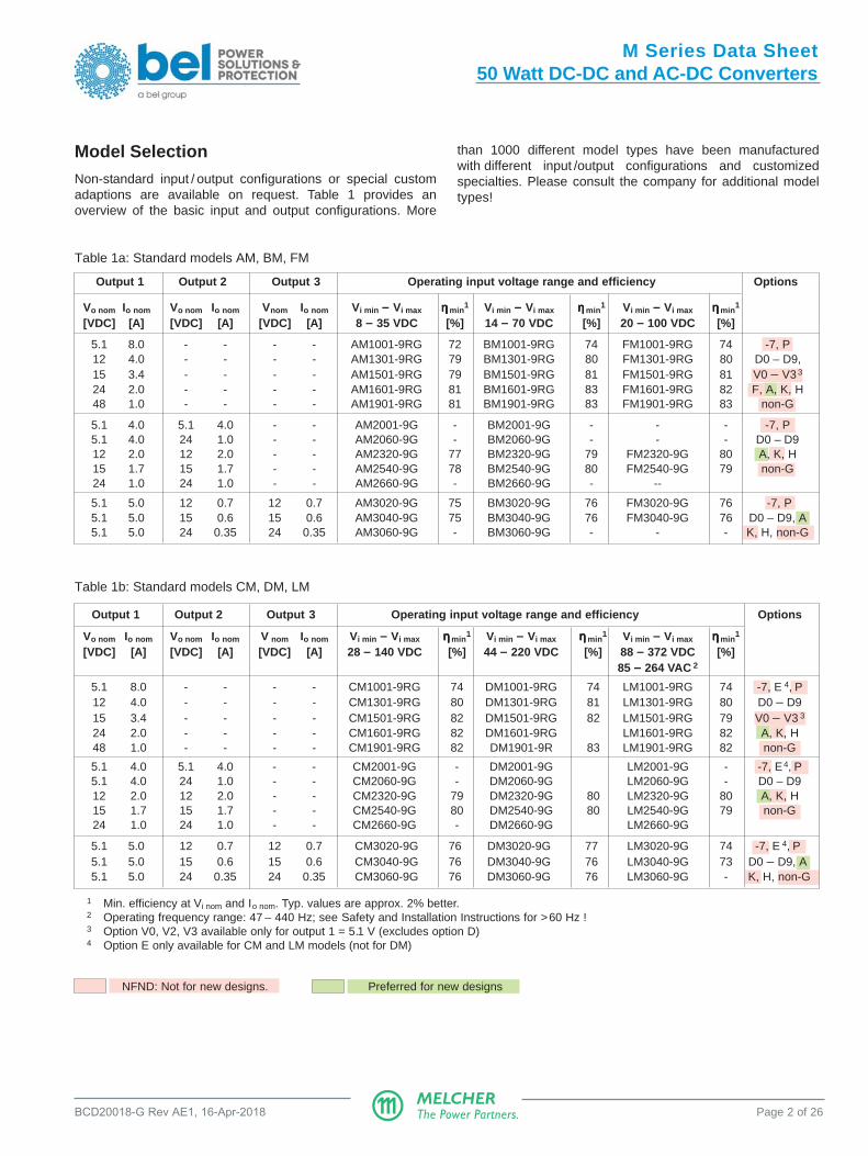
Model SelectionNon-standard input / output configurations or special customadaptions are available on request. Table 1 provides anoverview of the basic input and output configurations. More
Table 1a: Standard models AM, BM, FM
Output 1 Output 2 Output 3 Operating input voltage range and efficiency Options
Vo nom Io nom Vo nom Io nom V nom Io nom Vi min – Vi max ηηηηη min1 Vi min – Vi max ηηηηη min
than 1000 different model types have been manufacturedwith different input /output configurations and customizedspecialties. Please consult the company for additional modeltypes!
Table 1b: Standard models CM, DM, LM
Output 1 Output 2 Output 3 Operating input voltage range and efficiency Options
Vo nom Io nom Vo nom Io nom V nom Io nom Vi min – Vi max ηηηηη min1 Vi min – Vi max ηηηηη min
1 Min. efficiency at Vi nom and Io nom. Typ. values are approx. 2% better.2 Operating frequency range: 47 – 440 Hz; see Safety and Installation Instructions for >60 Hz !3 Option V0, V2, V3 available only for output 1 = 5.1 V (excludes option D)4 Option E only available for CM and LM models (not for DM)
NFND: Not for new designs. Preferred for new designs
M Series Data Sheet50 Watt DC-DC and AC-DC Converters
MELCHERThe Power Partners.BCD20018-G Rev AE1, 16-Apr-2018 Page 3 of 26
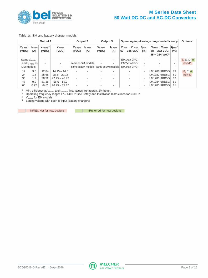
Table 1c: EM and battery charger models
Output 1 Output 2 Output 3 Operating input voltage range and efficiency Options
Vo Bat 3 Io nom Vo safe
4 Vo max Vo nom Io nom Vo nom Io nom Vi min – Vi max ηηηηη min 1 Vi min – Vi max ηηηηη min
1 Min. efficiency at Vi nom and Io nom. Typ. values are approx. 2% better.2 Operating frequency range: 47 – 440 Hz; see Safety and Installation Instructions for >60 Hz3 Vo nom for EM models4 Setting voltage with open R-input (battery chargers)
NFND: Not for new designs. Preferred for new designs
M Series Data Sheet50 Watt DC-DC and AC-DC Converters
MELCHERThe Power Partners.BCD20018-G Rev AE1, 16-Apr-2018 Page 4 of 26
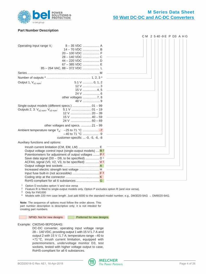
Example: CM2540-9EPD3AHG:DC-DC converter, operating input voltage range28 – 140 VDC, providing output 1 with 15 V/1.7 A andoutput 2 with 15 V /1.7 A; temperature range –40 to+71 °C, inrush current limitation, equipped withpotentiometers, undervoltage monitor D3, testsockets, tested with higher voltage output to case,RoHS-compliant for all 6 substances.
Part Number Description
C M 2 5 40 -9 E P D3 A H G
Operating input range Vi: 8 – 35 VDC ................... A14 – 70 VDC ................... B
12 V ........................20 – 3915 V ........................40 – 5924 V ........................60 – 69
other voltages and specs. ............21 – 99
Ambient temperature range TA: –25 to 71 °C .................. -7– 40 to 71 °C .................. -9
customer-specific ... -0, -5, -6, -8
Auxiliary functions and options:
Inrush current limitation (CM, EM, LM) ........................ EOutput voltage control input (single-output models) .... R 2Potentiometers for adjustment of output voltages ....... P 2Save data signal (D0 – D9, to be specified) ................ D 1ACFAIL signal (V0, V2, V3, to be specified) ................ V 1Output voltage test sockets .......................................... AIncreased electric strength test voltage ....................... H Input fuse built-in (not accessible) ............................... F 3Coding strip at the connector ....................................... KRoHS-compliant for all 6 substances ........................... G
1 Option D excludes option V and vice versa2 Feature R is fitted to single-output models only. Option P excludes option R (and vice versa).3 Only for FM10004 Models with 220 mm case length. Just add 6000 to the standard model number, e.g., DM3020-9AG → DM9020-9AG.
NFND: Not for new designs Preferred for new designs.
Note: The sequence of options must follow the order above. Thispart number description is descriptive only; it is not inteded forcreating part numbers.
M Series Data Sheet50 Watt DC-DC and AC-DC Converters
MELCHERThe Power Partners.BCD20018-G Rev AE1, 16-Apr-2018 Page 5 of 26
Functional DescriptionThe input voltage is fed via an input fuse, an input filter, a bridgerectifier, and an inrush current limiter to the input capacitor.This capacitor sources a single-transistor forward converter.Each output is powered by a separate secondary winding of themain transformer. The resultant voltages are rectified and theirripple smoothed by a power choke and an output filter. Themain control circuit senses the main output voltage Vo1 andgenerates, with respect to the maximum admissible output
currents, the control signal for the primary switching transistor.This signal is transferred to the primary side by a couplingtransformer.
The auxiliary output voltages Vo2 and Vo3 are individuallyregulated by means of secondary switching transistors. Eachauxiliary output's current is sensed using a current transformer.If one of the outputs is driven into current limit, the other outputswill reduce their output voltages as well, because all outputcurrents are controlled by the same main control circuit.
1 Transient suppressor diode in AM, BM, CM, FM models.2 Bridge rectifier in LM, series diode in EM models.3 Inrush current limiter (NTC) in CM, DM, EM, LM models (option E: refer to the description of option E).4 Single-output models with feature R.5 LM-models
Fig. 1
Block diagram, triple-output models
Inp
ut
filte
r
Output 1
filter
Output 3
filter
Output 2
filter
Control
circuit
output 3
Main control circuit
Control
circuit
output 2
1
Fu
se
Option P
29
11
8
23
5
26
32
17
14
20
2
14
17
3
2
Fo
rwa
rd c
on
ve
rte
r
ap
pro
x.
70
kH
z
4
4
CY
CY
CZ
CZ
Vi+
Vi–
i
D, V
R
G
03009a
5N
5
5L
M Series Data Sheet50 Watt DC-DC and AC-DC Converters
MELCHERThe Power Partners.BCD20018-G Rev AE1, 16-Apr-2018 Page 6 of 26
Table 2b: Input data
Input DM EM LM Unit
Characteristics Conditions min typ max min typ max min typ max
Vi Operating input voltage Io = 0 – Io nom - - 85 264 VAC 1
TC min – TC max 44 220 67 385 88 372 VDC
Vi nom Nominal input voltage 110 220 310
Ii Input current Vi nom, Io nom 2 0.55 0.275 0.20 A
Pi inh Idle input power inhibited, Vi nom 1 1.5 1 1.5 1 1.5
Iinr p 6 Peak inrush current Vi = Vi max 110 4 160 4 60 4 A
tinr r Rise time RS = 0 Ω 340 40 300 µs
tinr h Time to half-valueTC = 25 °C
250 240 900
Ri Input resistance TC = 25 °C 2000 4 2400 4 6200 4 mΩ
Ci Input capacitance 140 270 140 270 140 270 µF
Vi abs Input voltage limits 0 400 5 – 400 400 –400 400 VDCwithout any damage – – – – 0 284 VAC
1 In AC powered mode (LM models): Nominal input voltage range: 100 – 240 VAC, operating input frequency range: 47 – 440 Hz2 With multiple-output models, the same condition for each output applies.3 RS = source resistance.4 Value for initial switch-on cycle.5 1 s max., duty cycle 1% max.6 I inr p = V i / (Rs + Ri); see Inrush Current.7 140 V continuously. CM models with version V106 or greater (or with suffix /131) withstand 154 V for 2 s.
Electrical Input DataGeneral conditions:– TA = 25 °C, unless TC is specified.– Connector pins 2 and 23 interconnected, R input not connected; with option P: Vo = Vo nom
Table 2a: Input data
Input AM BM FM CM Unit
Characteristics Conditions min typ max min typ max min typ max min typ max
Vi Operating input voltage Io = 0 – Io nom 8 35 14 70 20 100 28 154 7 VDC
Vi nom Nominal input voltage TC min – TC max 15 30 50 60
Ii Input current Vi nom, Io nom 2 4.0 2.0 1.2 1.0 A
V i abs Input voltage limits 0 40 0 80 0 120 0 160 VDCwithout any damage
M Series Data Sheet50 Watt DC-DC and AC-DC Converters
MELCHERThe Power Partners.BCD20018-G Rev AE1, 16-Apr-2018 Page 7 of 26
Input Fuse
A fuse holder containing a slow-blow type fuse (size: 5 × 20mm) is mounted in the back plate of the converter. The fuseprotects the converter against severe defects. It may not fullyprotect it at input voltages exceeding 200 VDC. In applications,where the converters operate at DC source voltages above 200VDC, an external fuse or a circuit breaker at system levelshould be installed.
The fuse and a VDR form together with the input filter aneffective protection against high input transients.
Note: For applications, where the fuse should not be accessible;see Option F.
Table 3: Fuse types (slow-blow)
Series Schurter type Part number
AM1000 – 3000 SPT 10 A /250 V 0001.2514
BM1000 – 3000 SPT 8 A /250 V 0001.2513
FM1000 – 3000 SPT 5 A /250 V 0001.2511
CM1000 – 3000 SPT 3.15 A /250 V 0001.2509
DM1000 – 3000 SPT 2.5 A /250 V 0001.2508EM1000 – 3000LM1000 – 3000
Fig. 2
Typical input current versus relative input voltage atnominal output load
Vi DC________Vi min DC2 3 4 5 61
0.1
1.0
10
AM
Ii [A]
LM
BM
FM
CM
DM
EM
04014a
70 350
60 300
50 250
40 200
30 150
20 100
10 50
0
80 400
0 0.8
2.01.0
2.5
1.2
3.0
1.4
3.5
1.6
4.00.6
1.5
0.4
1.0
0.2
0.5
AM
BM
CM
FM
EM
A-EM
LM
Ii [A]
LM
DM
t [ms]
LM A-EM04015a
Input Under-/Overvoltage Lockout
If the input voltage remains below 0.8 Vi min or exceeds approx.1.1 Vi max, an internally generated inhibit signal disables theoutput(s). When checking this function the absolute maximuminput voltage rating Vi abs must be carefully considered (seetable Input data).
Note: When Vi is between Vi min and the undervoltage lockout level,the output voltage may be below the value defined in table Outputdata.
Reverse Polarity
Reverse polarity at the input of AM, BM, CM, DM, and FMmodels will cause the fuse to blow. In EM and LM models aseries diode will protect the converter. A series diode is notincorporated in AM, BM, CM, DM and FM types to avoidunwanted power losses.
Inrush Current
The CM, DM, EM, and LM (excluding FM) models incorporatean NTC resistor in the input line, which (during the initial switch-on cycle) limits the peak inrush current in order to prevent theconnectors and external switching devices from damage.Subsequent switch-on cycles within a short interval will causean increase of the peak inrush current due to the warming-up ofthe NTC resistor. Refer to Option E (only available for CM, EM,and LM.
Fig. 3
Typical inrush current at initial switch-on. Vi max (DC) andnominal output load
M Series Data Sheet50 Watt DC-DC and AC-DC Converters
MELCHERThe Power Partners.BCD20018-G Rev AE1, 16-Apr-2018 Page 8 of 26
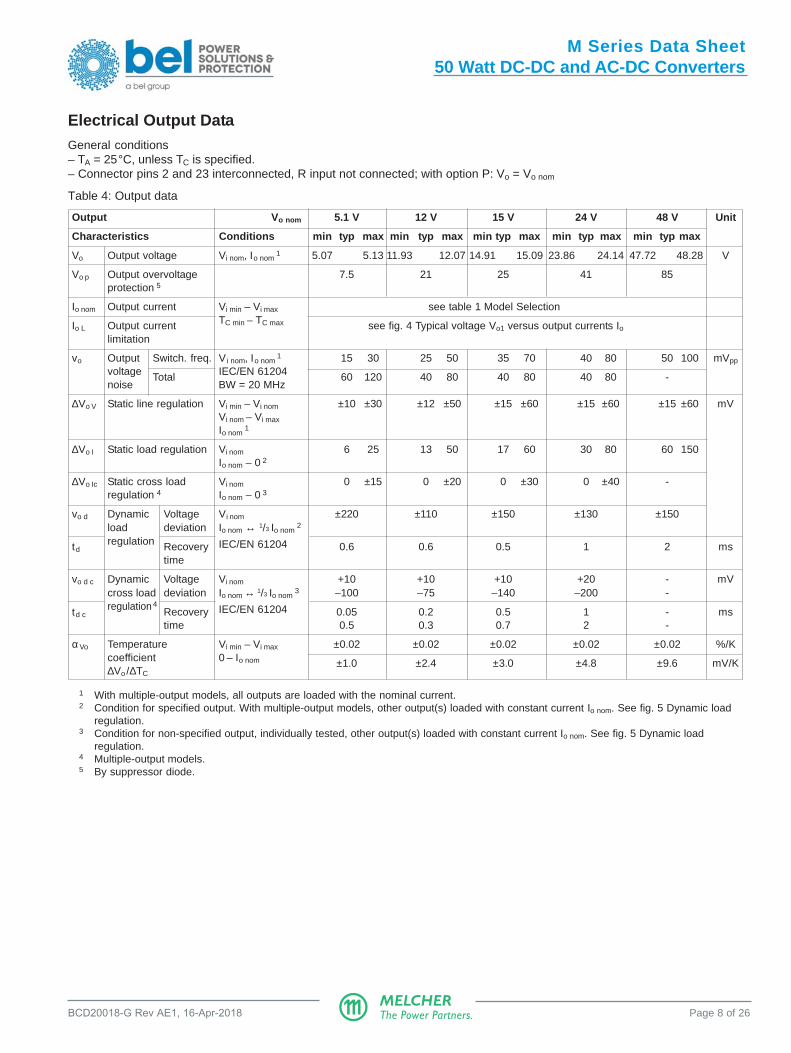
Electrical Output DataGeneral conditions– TA = 25°C, unless TC is specified.– Connector pins 2 and 23 interconnected, R input not connected; with option P: Vo = Vo nom
Table 4: Output data
Output Vo nom 5.1 V 12 V 15 V 24 V 48 V Unit
Characteristics Conditions min typ max min typ max min typ max min typ max min typ max
Vo Output voltage Vi nom, Io nom 1 5.07 5.13 11.93 12.07 14.91 15.09 23.86 24.14 47.72 48.28 V
Vo p Output overvoltage 7.5 21 25 41 85protection 5
Io nom Output current Vi min – Vi max see table 1 Model Selection
Io L Output current TC min – TC max see fig. 4 Typical voltage Vo1 versus output currents Iolimitation
vo Output Switch. freq. V i nom, Io nom 1 15 30 25 50 35 70 40 80 50 100 mVpp
voltage Total IEC/EN 61204 60 120 40 80 40 80 40 80 -noise BW = 20 MHz
∆Vo V Static line regulation Vi min – Vi nom ±10 ±30 ±12 ±50 ±15 ±60 ±15 ±60 ±15 ±60 mVVi nom – Vi max
Io nom 1
∆Vo I Static load regulation Vi nom 6 25 13 50 17 60 30 80 60 150Io nom – 0 2
∆Vo Ic Static cross load Vi nom 0 ±15 0 ±20 0 ±30 0 ±40 -regulation 4 Io nom – 0 3
vo d Dynamic Voltage Vi nom ±220 ±110 ±150 ±130 ±150load deviation Io nom ↔ 1/3 Io nom
2
tdregulation Recovery IEC/EN 61204 0.6 0.6 0.5 1 2 ms
time
vo d c Dynamic Voltage Vi nom +10 +10 +10 +20 - mVcross load deviation Io nom ↔ 1/3 Io nom
α Vo Temperature Vi min – Vi max ±0.02 ±0.02 ±0.02 ±0.02 ±0.02 %/Kcoefficient 0 – Io nom ±1.0 ±2.4 ±3.0 ±4.8 ±9.6 mV/K∆Vo /∆TC
1 With multiple-output models, all outputs are loaded with the nominal current.2 Condition for specified output. With multiple-output models, other output(s) loaded with constant current Io nom. See fig. 5 Dynamic load
regulation.3 Condition for non-specified output, individually tested, other output(s) loaded with constant current Io nom. See fig. 5 Dynamic load
regulation.4 Multiple-output models.5 By suppressor diode.
M Series Data Sheet50 Watt DC-DC and AC-DC Converters
MELCHERThe Power Partners.BCD20018-G Rev AE1, 16-Apr-2018 Page 9 of 26
Fig. 6
Output current derating versus temperature
Fig. 4
Typical voltage Vo versus output currents Io.
Fig. 5
Dynamic load regulation Vo d versus load change.
1.0
0
0.5
Vo
0.5
Vo nom
Io
Io nom1.0 1.2
Io nom
Io1
Io2,Io3
IoL1
IoL2, IoL3
0.95
05022a
Io/Io nom
1
Vod
Vodtd td
∆Vo I ∆Vo I
t
Vo
0 t
≥10 µs≥10 µs05010a
0.3
Output Characteristic and Protection
Each output is protected by a suppressor diode, which underworst case conditions may become a short circuit. Thesuppressor diodes are not designed to withstand externallyapplied overvoltages. Overload at any of the outputs will causea shutdown of all outputs. A red LED indicates an overloadcondition at the respective output.
Thermal Considerations and Protection
If a converter is located in free, quasi-stationary air (convectioncooling) at the indicated maximum ambient temperature TA max
(see table Temperature specifications) and is operated at itsnominal input voltage and output power, the temperaturemeasured at the measuring point of case temperature TC (seeMechanical Data) will approach the indicated value TC max afterthe warm-up phase. However, the relationship between TA andTC depends heavily on the conditions of operation andintegration into a system. The thermal conditions areinfluenced by input voltage, output current, airflow, and
temperature of surrounding components and surfaces. TA max istherefore, contrary to TC max, an indicative value only.
Caution: The installer must ensure that under all operatingconditions TC remains within the limits stated in the tableTemperature specifications.
Notes: Sufficient forced cooling or an additional heat sink allow TA
to pass over 71 °C, if TC max is not exceeded.
For -7 or -9 models at an ambient temperature TA of 85 °C withonly convection cooling, the maximum permissible current foreach output is approx. 50% of its nominal value; see figure 6.
A temperature sensor generates an internal inhibit signaldisabling the outputs, when the case temperature exceedsTC max. The outputs automatically recover, when thetemperature drops below this limit.
Parallel and Series Connection
Main outputs of equal nominal voltage can be connected inparallel. It is important to assure that the main output of amultiple-output converter is forced to supply a minimum currentof 0.1 A to enable correct operation of its own auxiliary outputs.
In parallel operation, one or more of the main outputs mayoperate continuously in current limitation, causing an increaseof the case temperature TC. Consequently, a reduction of themax. ambient temperature by 10 K is recommended.
Main or auxiliary outputs can be connected in series with anyother output of the same or another converter. In seriesconnection, the maximum output current is limited by thelowest current limit. Output ripple and regulation values areadded. Connection wiring should be kept as short as possible.
If output terminals are connected together in order to establishmulti-voltage configurations, e.g., +5.1 V, ±12 V etc., thecommon-ground connecting point should be as close aspossible to the connectors of the converter in order to avoidexcessive output ripple voltages.
Note: Auxiliary outputs should never be connected in parallel!
0
0.2
0.4
0.6
0.8
50 60 70 80 90 100
Io/Io nom
TA [°C]
1.0Forced cooling
05031a
TC max
Convection cooling
M Series Data Sheet50 Watt DC-DC and AC-DC Converters
MELCHERThe Power Partners.BCD20018-G Rev AE1, 16-Apr-2018 Page 10 of 26
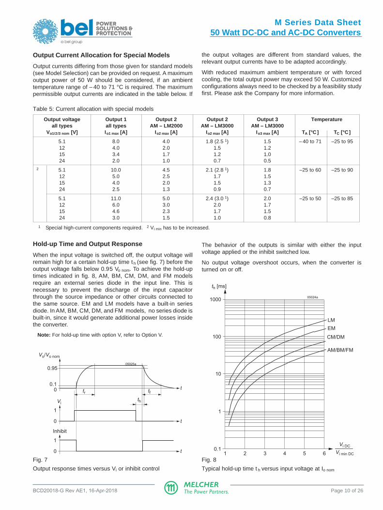
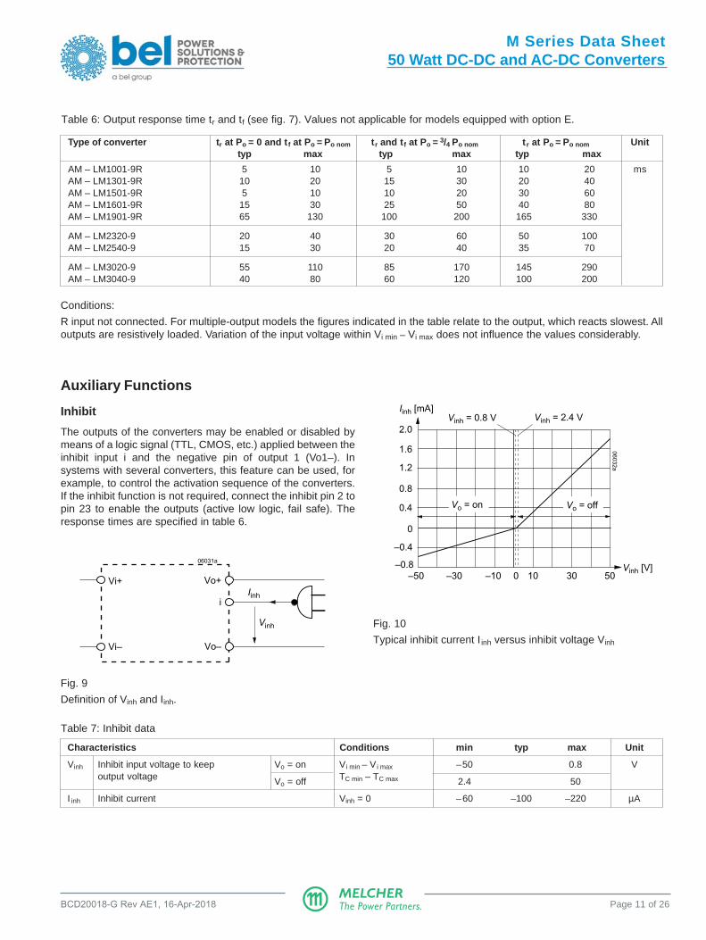
Hold-up Time and Output Response
When the input voltage is switched off, the output voltage willremain high for a certain hold-up time t h (see fig. 7) before theoutput voltage falls below 0.95 Vo nom. To achieve the hold-uptimes indicated in fig. 8, AM, BM, CM, DM, and FM modelsrequire an external series diode in the input line. This isnecessary to prevent the discharge of the input capacitorthrough the source impedance or other circuits connected tothe same source. EM and LM models have a built-in seriesdiode. In AM, BM, CM, DM, and FM models, no series diode isbuilt-in, since it would generate additional power losses insidethe converter.
Note: For hold-up time with option V, refer to Option V.
The behavior of the outputs is similar with either the inputvoltage applied or the inhibit switched low.
No output voltage overshoot occurs, when the converter isturned on or off.
Fig. 7
Output response times versus Vi or inhibit control
Fig. 8
Typical hold-up time t h versus input voltage at Io nom
Output Current Allocation for Special Models
Output currents differing from those given for standard models(see Model Selection) can be provided on request. A maximumoutput power of 50 W should be considered, if an ambienttemperature range of – 40 to 71 °C is required. The maximumpermissible output currents are indicated in the table below. If
the output voltages are different from standard values, therelevant output currents have to be adapted accordingly.
With reduced maximum ambient temperature or with forcedcooling, the total output power may exceed 50 W. Customizedconfigurations always need to be checked by a feasibility studyfirst. Please ask the Company for more information.
Table 5: Current allocation with special models
Output voltage Output 1 Output 2 Output 2 Output 3 Temperatureall types all types AM – LM2000 AM – LM3000 AM – LM3000
Vo1/2/3 nom [V] Io1 max [A] Io2 max [A] Io2 max [A] Io3 max [A] TA [°C ] TC [°C]
R input not connected. For multiple-output models the figures indicated in the table relate to the output, which reacts slowest. Alloutputs are resistively loaded. Variation of the input voltage within Vi min – Vi max does not influence the values considerably.
Auxiliary Functions
Inhibit
The outputs of the converters may be enabled or disabled bymeans of a logic signal (TTL, CMOS, etc.) applied between theinhibit input i and the negative pin of output 1 (Vo1–). Insystems with several converters, this feature can be used, forexample, to control the activation sequence of the converters.If the inhibit function is not required, connect the inhibit pin 2 topin 23 to enable the outputs (active low logic, fail safe). Theresponse times are specified in table 6.
Fig. 9
Definition of Vinh and Iinh.
Fig. 10
Typical inhibit current I inh versus inhibit voltage Vinh
Table 7: Inhibit data
Characteristics Conditions min typ max Unit
Vinh Inhibit input voltage to keep Vo = on Vi min – V i max –50 0.8 Voutput voltage Vo = off TC min – TC max 2.4 50
I inh Inhibit current Vinh = 0 –60 –100 –220 µA
1.6
0.8
0
–0.8–50
Vinh [V]
Iinh [mA]
–30 0–10 10 30 50
2.0
1.2
0.4
–0.4
Vinh = 0.8 V
Vo = on Vo = off
Vinh = 2.4 V
06032a
M Series Data Sheet50 Watt DC-DC and AC-DC Converters
MELCHERThe Power Partners.BCD20018-G Rev AE1, 16-Apr-2018 Page 12 of 26
Table 8a: Rext1 for Vo < Vo nom (conditions: Vi nom, Io nom, rounded up to resistor values E 96, Rext2 is not fitted.)
Vo nom = 5.1 V Vo nom = 12 V Vo nom = 15 V Vo nom = 24 V Vo nom = 48 VVo [V] Rext1 [kΩ] Vo [V] Rext1 [kΩ] Vo [V] Rext1 [kΩ] Vo [V] Rext1 [kΩ] Vo [V] Rext1 [kΩ]
Table 8b: R2 for Vo > Vo nom (conditions: Vi nom, Io nom, rounded up to resistor values E 96, Rext1 is not fitted.)
Vo nom = 5.1 V Vo nom = 12 V Vo nom = 15 V Vo nom = 24 V Vo nom = 48 VVo [V] Rext2 [kΩ] Vo [V] Rext2 [kΩ] Vo [V] Rext2 [kΩ] Vo [V] Rext2 [kΩ] Vo [V] Rext2 [kΩ]
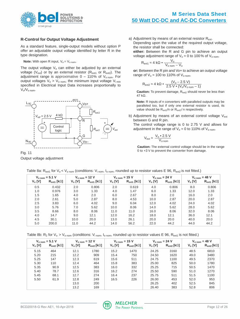
As a standard feature, single-output models without option Poffer an adjustable output voltage identified by letter R in thetype designation.
Note: With open R input, Vo = Vo nom.
The output voltage Vo can either be adjusted by an externalvoltage (Vext) or by an external resistor (Rext1 or Rext2). Theadjustment range is approximative 0 – 110% of Vo nom. Foroutput voltages Vo > Vo nom, the minimum input voltage Vi min
specified in Electrical Input Data increases proportionally toVo/Vo nom.
Fig. 11
Output voltage adjustment
a) Adjustment by means of an external resistor Rext.Depending upon the value of the required output voltage,the resistor shall be connected:either: Between the R and G pin to achieve an outputvoltage adjustment range of Vo ≈ 0 to 100 % of Vo nom.
VoRext1 ≈ 4 kΩ • ––––––––– Vo nom – Vo
or: Between the R pin and Vo+ to achieve an output voltagerange of Vo ≈ 100 to 110% of Vo nom.
(Vo – 2.5 V)Rext2 ≈ 4 kΩ • ––––––––––––––––––
2.5 V • (Vo/Vo nom – 1)
Caution: To prevent damage, Rext2 should never be less than47 kΩ.
Note: R inputs of n converters with paralleled outputs may beparalleled too, but if only one external resistor is used, itsvalue should be Rext1/n or Rext2/ n respectively.
b) Adjustment by means of an external control voltage Vext
between G and R pin.The control voltage range is 0 to 2.75 V and allows foradjustment in the range of Vo ≈ 0 to 110% of Vo nom.
Vo • 2.5 VVext ≈ ––––––––
Vo nom
Caution: The external control voltage should be in the range0 to +3 V to prevent the converter from damage.
R
Vo+
Vo–
+
Vext
–
4 kΩVref = 2.5 V
Control
logic Rext1
Rext2
JM075
+
G
L
N
M Series Data Sheet50 Watt DC-DC and AC-DC Converters
MELCHERThe Power Partners.BCD20018-G Rev AE1, 16-Apr-2018 Page 13 of 26
Display Status of LEDs
LEDs "OK" and "i" status versus input voltage Vi
Conditions: Io ≤ Io nom , TC ≤ TC max , Vinh ≤ 0.8 V
Vi uv = undervoltage lockout, Vi ov = overvoltage lockout
LEDs "OK" and "Io L" status versus output current Io
Conditions: Vi min – Vi max , TC ≤ TC max , Vinh ≤ 0.8 V
LED "i" versus case temperature
Conditions: Vi min – Vi max , Io ≤ Io nom , Vinh ≤ 0.8 V
LED "i" versus Vinh
Conditions: Vi min – Vi max , Io ≤ Io nom , TC ≤ TC max
Vo1 > 0.95 to 0.98 Vo1 adj
Vi max Vi ovVi minVi uv
Vi
Vi abs
OK
i
Vo1 > 0.95 to 0.98 Vo1 adj
Io nom IoL
Io
OK
Io L
Vo1 < 0.95 to 0.98 Vo1 adj
TC
i
TC max TPTC threshold
Vinh
i
+50 V+0.8 V +2.4 V-50 V
Vinh threshold
Io L
LED off LED onLED status undefined
06002a
Fig. 12
Status of LEDs.
M Series Data Sheet50 Watt DC-DC and AC-DC Converters
MELCHERThe Power Partners.BCD20018-G Rev AE1, 16-Apr-2018 Page 14 of 26
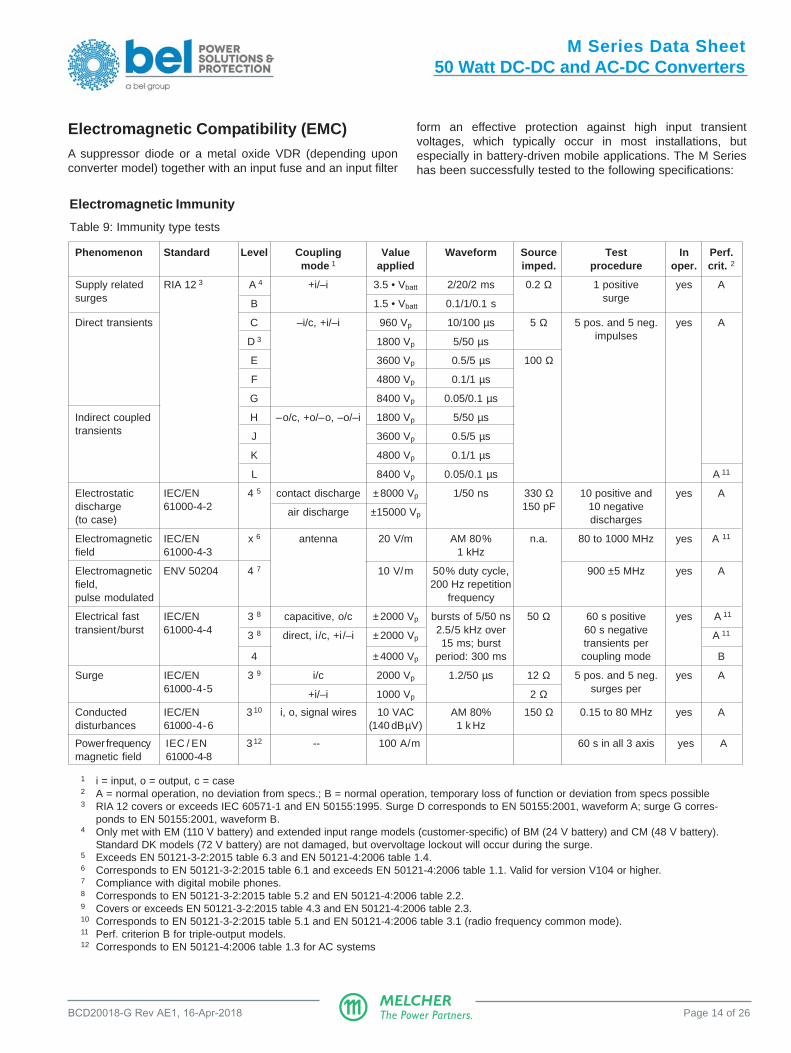
Electromagnetic Immunity
Table 9: Immunity type tests
Phenomenon Standard Level Coupling Value Waveform Source Test In Perf.mode 1 applied imped. procedure oper. crit. 2
Supply related RIA 12 3 A 4 +i/–i 3.5 • Vbatt 2/20/2 ms 0.2 Ω 1 positive yes Asurges B 1.5 • Vbatt 0.1/1/0.1 s surge
Direct transients C –i/c, +i/–i 960 Vp 10/100 µs 5 Ω 5 pos. and 5 neg. yes A
Conducted IEC/EN 3 10 i, o, signal wires 10 VAC AM 80% 150 Ω 0.15 to 80 MHz yes Adisturbances 61000-4-6 (140 dBµV) 1 k Hz
Power frequency IEC / EN 3 12 -- 100 A/m 60 s in all 3 axis yes Amagnetic field 61000-4-8
1 i = input, o = output, c = case2 A = normal operation, no deviation from specs.; B = normal operation, temporary loss of function or deviation from specs possible3 RIA 12 covers or exceeds IEC 60571-1 and EN 50155:1995. Surge D corresponds to EN 50155:2001, waveform A; surge G corres-
ponds to EN 50155:2001, waveform B.4 Only met with EM (110 V battery) and extended input range models (customer-specific) of BM (24 V battery) and CM (48 V battery).
Standard DK models (72 V battery) are not damaged, but overvoltage lockout will occur during the surge.5 Exceeds EN 50121-3-2:2015 table 6.3 and EN 50121-4:2006 table 1.4.6 Corresponds to EN 50121-3-2:2015 table 6.1 and exceeds EN 50121-4:2006 table 1.1. Valid for version V104 or higher.7 Compliance with digital mobile phones.8 Corresponds to EN 50121-3-2:2015 table 5.2 and EN 50121-4:2006 table 2.2.9 Covers or exceeds EN 50121-3-2:2015 table 4.3 and EN 50121-4:2006 table 2.3.10 Corresponds to EN 50121-3-2:2015 table 5.1 and EN 50121-4:2006 table 3.1 (radio frequency common mode).11 Perf. criterion B for triple-output models.12 Corresponds to EN 50121-4:2006 table 1.3 for AC systems
Electromagnetic Compatibility (EMC)A suppressor diode or a metal oxide VDR (depending uponconverter model) together with an input fuse and an input filter
form an effective protection against high input transientvoltages, which typically occur in most installations, butespecially in battery-driven mobile applications. The M Serieshas been successfully tested to the following specifications:
M Series Data Sheet50 Watt DC-DC and AC-DC Converters
MELCHERThe Power Partners.BCD20018-G Rev AE1, 16-Apr-2018 Page 15 of 26
PMM 8000 PLUS: Peak, conducted Vi+, QP + AV, 2011-08-02, 10:48 hCM1601-9ER, Ui=60 V, Uo=24 V Io= 2 A
0
dBµV
20
40
60
80
0.2 0.5 1 2 5 10 20 MHz
JM131
EN 55022 A (qp)
EN 55022 A (av)
Electromagnetic Emissions
Fig. 13a
Typ. conducted disturbances at the input (quasi-peak andaverage) of CM1601-9ER according to IEC/EN 55011/22,measured at Vi = 60 VDC and Io nom.
Fig. 14b
Typical radiated emissions of LM1601-9R according to IEC/EN 55011/22, normalized to a distance of 10 m, measured atVi = 230 VAC and Io nom.
30 50 100 200 500 1000 MHz
dBµV/m
10
20
30
40
0
50
TÜV-Divina, ESVS 30:R&S, BBA 9106/UHALP 9107:Schwarzb., QP, 2011-08-02Testdistance 10 m, LM1601-9R, Ui=230 VAC, Uo=24 V Io= 2 A
JM129
EN 55011 A
<25 dbµV/m
Fig. 14a
Typical radiated emissions of CM1601-9ER according to IEC/EN 55011/22, normalized to a distance of 10 m, measured atVi = 60 VDC and Io nom.
30 50 100 200 500 1000 MHz
dBµV/m
10
20
30
40
0
50
TÜV-Divina, ESVS 30:R&S, BBA 9106/UHALP 9107:Schwarzb., QP, 2011-08-03Testdistance 10 m, CM1601-9ER, Ui= 60 VDC, Uo=24 V Io= 2 A
JM130
EN 55011 A
<25 dbµV/m
Fig. 13b
Typ. conducted disturbances at the input (quasi-peak andaverage) of LM1601-9R according to IEC/EN 55011/22,measured at Vi = 230 VAC and Io nom.
PMM 8000 PLUS: Peak, conducted Vi+, QP + AV, 2011-08-02, 10:48 hCM1601-9ER, Ui=60 V, Uo=24 V Io= 2 A
0
dBµV
20
40
60
80
0.2 0.5 1 2 5 10 20 MHz
JM132
EN 55022 A (qp)
EN 55022 A (av)
M Series Data Sheet50 Watt DC-DC and AC-DC Converters
MELCHERThe Power Partners.BCD20018-G Rev AE1, 16-Apr-2018 Page 16 of 26
Immunity to Environmental ConditionsTable 10: Mechanical and climatic stress
Test method Standard Test conditions Status
Db Damp heat test, EN 50155:2007, clause 12.2.5 Temperature: 55 °C and 25 °C Convertercyclic IEC/EN 60068-2-30 Cycles (respiration effect): 2 not
Duration: 2× 24 h operating
Bd Dry heat test EN 50155:2007, clause 12.2.4 Temperature: 70 °C Convertersteady state IEC/EN 60068-2-2 Duration: 6 h operating
Ad Cooling test EN 50155:2007, clause 12.2.3 Temperature, duration –40 °C, 2 h Conv. notsteady state IEC/EN 60068-2-1 Performance test +25 °C operating
Kb Salt mist, cyclic IEC/EN 60068-2-52 Concentration: 5% (30 °C) Converter(sodium chloride Duration: 2 h per cycle notNaCl solution) Storage: 40°C, 93% rel. humidity operating
Storage duration: 22 h per cycle, 3 cycles
Fc Vibration IEC/EN 60068-2-6 Acceleration amplitude: 0.35 mm (10 – 60 Hz) Converter(sinusoidal) MIL-STD-810D section 514.3 5 gn = 49 m/s2 (60 – 2000 Hz) operating
Frequency (1 Oct/min): 10 – 2000 HzTest duration: 7.5 h (2.5 h each axis)
Fda Random vibration IEC 60068-2-35 Acceleration spectral density: 0.05 gn2/Hz Converter
wide band DIN 40046 part 23 Frequency band: 20 – 500 Hz operatingReproducibility Acceleration magnitude: 4.9 g n rms
high Test duration: 3 h (1 h each axis)
Eb Bump IEC/EN 60068-2-29 Acceleration amplitude: 40 gn = 392 m/s2 Converter(half-sinusoidal) MIL-STD-810D section 516.3 Bump duration: 6 ms operating
Number of bumps: 6000 (1000 each direction)
Ea Shock IEC/EN 60068-2-27 Acceleration amplitude: 100 gn = 981 m/s2 Converter(half-sinusoidal) MIL-STD-810D section 516.3 Bump duration: 6 ms operating
Number of bumps: 18 (3 each direction)
-- Shock EN 50155:2007 clause 12.2.11, Acceleration amplitude: 5.1 gn ConverterEN 61373 sect. 10, Bump duration: 30 ms operatingclass B, body mounted 1 Number of bumps: 18 (3 in each direction)
-- Simulated long life EN 50155:2007 clause 12.2.11, Acceleration spectral density: 0.02 gn2 / Hz Converter
testing at EN 61373 sect. 8 and 9, Frequency band: 5 – 150 Hz operatingincreased random class B, body mounted 1 Acceleration magnitude: 0.8 gn rms
vibration levels Test duration: 15 h (5 h in each axis)
1 Body mounted = chassis of a railway coach
ReliabilityTable 12: MTBF
Values at specified Converter model Ground benign Ground fixed Ground mobile Device hours 2 Unitcase temperature 40 °C 40 °C 70 °C 50 °C
1 Calculated in accordance with MIL-HDBK-217E2 Statistical values, based on an average of 4300 working hours per year in general field use over 3 years
TemperaturesTable 11: Temperature specifications, valid for an air pressure of 800 – 1200 hPa (800 – 1200 mbar)
Temperature -7 (option) - 9 (standard) Unit
Characteristics Conditions min max min max
TA Ambient temperature Operational –25 71 –40 71 °C
TC Case temperature –25 95 –40 95
TS Storage temperature Non operational –40 85 –55 85
M Series Data Sheet50 Watt DC-DC and AC-DC Converters
MELCHERThe Power Partners.BCD20018-G Rev AE1, 16-Apr-2018 Page 17 of 26
Mechanical DataDimensions in mm. European
Projection
Fig. 15
Case M02, weight 770 g (approx.).
Case aluminum, black finish and selfcooling.
Note: Long case, elongated by 60mm for 220 mm rack depth, isavailable on request.
111.2 ±0.8 (3 U)
88(11.6)
168.5
127
173.7
±0.5
20
100 ±0.6
1.6
6T
E
2 5 8 11
14
17
20
23
26
29
32
Male connector H11 according to DIN 41612
38.7
95 ±0.5
Measuring point for
case temperatureTC
M 3; depth = 4 mm
(chassis mount)
22
68
159.4
Mounting plane of
connector H11
5.0
8
10.1
6
15.2
420.3
225.4
030.4
8
2T
E
7.09
17.25
28.6
34
15
4
Mounting holes for connector retention clips
12.17
103
3.2
7
20.5
12.1
94.5 ±0.1
0
31.5
±0.1
0
ø 3
.5
ø 4
.0
IoL (LED red)
Test sockets (option A)
Potentiometer(s) (option P)
Inhibit i (LED red)
OK (LED green)
Potentiometer
(option D or V)
Front plate
Main
faceRear
face
Back plate
22.30
09
01
2c
Caution! Gets hot!
OK
i
1 2 3
I oL
M Series Data Sheet50 Watt DC-DC and AC-DC Converters
MELCHERThe Power Partners.BCD20018-G Rev AE1, 16-Apr-2018 Page 18 of 26
Safety and Installation Instructions
Connector Pin Allocation
Pin no. 26 (protective earth) is a leading pin, ensuring that itmakes contact with the female connector first.
Table 13: Pin allocation Fig. 16
View of male H11 connector.
Installation Instructions
All M Series converters are components, intended exclusivelyfor inclusion within other equipment by professional installers.Installation must strictly follow the national safety regulations incompliance with the enclosure, mounting, creepage,clearance, casualty, markings and segregation requirements ofthe end-use application.
Connection to the system shall be made via the femaleconnector H11. Other installation methods may not meet thesafety requirements.
The converters are provided with the leading pin 26 ( ), whichis reliably connected with the case. For safety reasons, it isessential to connect pin 26 with the protective earth of thesupply system.
An input fuse is connected in the line to pin 32 (Vi– or L ).Since this fuse is designed to protect the converter in case ofan overcurrent and does not necessarily cover all customerneeds, an external fuse suitable for the application and incompliance with the local requirements may be necessary inthe wiring to one or both input pins (no. 29 and/or no. 32),particularly if the phase or neutral line cannot be assigned tothe corresponding terminals (LM models operated with AC).
Important: Whenever the inhibit function is not in use,pin 2 (i) should be connected to pin 23 (Vo–) to enablethe output(s).
Caution: Do not open the converters, or warranty willbe invalidated.
Make sure that there is sufficient air flow possible forconvection cooling. This should be verified bymeasuring the case temperature TC, when theconverter is installed and operated in the end-useapplication. The maximum specified casetemperature TC max shall not be exceeded. See alsoThermal Considerations.
Operation of LM Models at Greater than 63 Hz
In such a case, the converters may exceed theleakage current of 3.5 mA imposed in the safetystandards. A warning marking is required in the end-use product.
Protection Degree and Cleaning Liquids
Condition: Female connector fitted to the converter.
IP 40: All models, except those with options P or A, andexcept those with option D/V with potentiometer.
IP 30: All models fitted with options A or option D/V withoutpotentiometer.
IP 20: All models fitted with option P or with option D/V withpotentiometer.
In order to avoid possible damage, any penetration of liquids(e.g., cleaning fluids) has to be avoided.
Railway Applications
The M Series converters have been designed observing therailway standards EN 50155 and EN 50121. All boards arecoated with a protection lacquer.
Standards and Approvals
The converters correspond to class I equipment and have beenapproved according to the standards IEC/EN 60950-1 and UL/CSA 60950-1 2nd Ed.
The converters have been evaluated for:
• Class I equipment• Building in• Basic insulation between input and case and double or
reinforced insulation between input and output, based on
Electrical determination AM – LM1000 AM – LM2000 AM – LM3000Pin Ident Pin Ident Pin Ident
Inhibit 2 i 2 i 2 iSafe Data or ACFAIL 5 5 D or V 5 5 D or V 5 5 D or V
Output voltage (positive) 8 Vo+ 8 n.c. 8 Vo3+Output voltage (negative) 11 Vo– 11 n.c. 11 Vo3–
Voltage adjust 14 R 1
Adjust return 17 G 1
Output voltage (positive) 14 Vo2+ 14 Vo2+Output voltage (negative) 17 Vo2– 17 Vo2–
Output voltage (positive) 20 Vo+ 20 Vo1+ 20 Vo1+Output voltage (negative) 23 Vo– 23 Vo1– 23 Vo1–
Protective earth PE 2 26 26 26
DC input voltage 3 29 Vi+ 29 Vi+ 29 Vi+DC input voltage 32 Vi– 32 Vi– 32 Vi–
AC input voltage 4 29 N 29 N 29 NAC input voltage 32 L 32 L 32 L
1 Not connected if option P is fitted2 Leading pin3 AM, BM, CM, DM, EM, and FM models4 LM models5 Not connected if option neither option D or V is fitted
32 29 26 23 20 17 14 11 8 5 2
10015aCaution! Gets hot!
M Series Data Sheet50 Watt DC-DC and AC-DC Converters
MELCHERThe Power Partners.BCD20018-G Rev AE1, 16-Apr-2018 Page 19 of 26
Safety of Operator-Accessible Output Circuits
If the output circuit of a DC-DC converter is operator-accessible, it shall be an SELV circuit according to the IEC/EN60950 safety standards.
Since the M Series converters provide double or reinforcedinsulation between input and output based upon a ratedprimary input voltage of 250 VAC or 400 VDC, only functional
the input voltage of 250 VAC or 400 VDC• Functional insulation between output(s) and case• Functional insulation between the outputs• Pollution degree 2 environment• Overvoltage category II• Altitude up to 2000 m
The converters are subject to manufacturing surveillance inaccordance with the above mentioned standards and with ISO9001:2008.
Isolation
The electric strength test is performed in the factory as routinetest in accordance with EN 50514 and IEC/EN 60950. Thecompany will not honor any warranty claims resulting fromincorrectly executed electric strength field tests.
Fig. 17
Schematic safety concept
AC-DC
front
end
DC-DC
con-
verter
Mains Battery SELV
Earth connection
+
–
~
~
10018a
Max. 250 VAC or
400 VDC
Max. 250 VAC or
400 VDC
Fuse
Fuse
+
Table 14: Isolation
Characteristic Input to case Output(s) to Output(s) to Output to Unitand output(s) case (standard) case (option H) output
Electric Factory test >1 s 2.8 1 1.4 2.8 0.3 kVDCstrength AC test voltage equivalent
2.0 1.0 2.0 0.2 kVACtest to factory test
Insulation resistance at 500 VDC >300 >300 >300 >100 2 MΩCreepage distances ≥ 3.2 3 -- -- -- mm
1 According to IEC/EN 60950, subassemblies connecting input to output are pre-tested with 5.6 kVDC or 4 kVAC.2 Tested at 300 VDC3 Input to outputs: ≥6.4 mm
Table 15: Safety concept leading to an SELV output circuit
Conditions Front end DC-DC converter Result
Nominal Minimum required grade Maximum rated Minimum required Equip- Measures to achieve the Safety statussupply of insulation, to be pro- DC output voltage safety status of the ment specified safety status of of the DC-DCvoltage vided by the AC-DC front from the front end front end output the output circuit converter
end, including mains circuit output circuitsupplied battery charger
Mains Operational (i.e. there is 400 VDC 1 (The Primary circuit A – LM Double or reinforced SELV circuit250 VAC no need for electrical rated voltage insulation, based on
isolation between the between any input 250 VAC and 400 VDCmains supply voltage and pin and earth can (provided by the DC-DCtheDC-DC converter be up to 250 VAC converter) and earthedinput voltage) or 400 VDC.) case 2
1 The front end output voltage should match the specified operating input voltage range of the DC-DC converter.2 The earth connection has to be provided by the installer according to the safety standard IEC/EN 60950.
insulation is needed between the AC mains and the input of theconverter. Only voltage adaption and rectification to thespecified input voltage range of a DC/DC converter is needed.
Table 15 shows a possible installation configuration, com-pliance with which causes the output circuit of the DC-DCconverter to be an SELV circuit according to IEC/EN 60950 upto a configured output voltage (sum of nominal voltages if inseries or +/– configuration) of 48 V. However, it is the soleresponsibility of the installer to assure the compliance with therelevant and applicable safety regulations.
M Series Data Sheet50 Watt DC-DC and AC-DC Converters
MELCHERThe Power Partners.BCD20018-G Rev AE1, 16-Apr-2018 Page 20 of 26
-7 Former Standard Temperature Range
Option -7 stays for the operational ambient temperature rangefrom –25 to 71 °C, which may be preferred by some customersfor reasons of documentation or approvals.
A Test Sockets
Test sockets (pin Ø = 2 mm, distance d = 5.08 mm) are locatedat the front of the converter. The output voltage is sensed at theconnector pins inside of the converter. Outputs 2 and 3 of triple-output models are not sensed.
P Potentiometer
Built-in multi-turn potentiometers provide an output voltageadjustment range of minimum ±5% of Vo nom and areaccessible through holes in the front cover. Compensation ofvoltage drop across connector and wiring becomes easilyachievable. For output voltages Vo > Vo nom, the minimum inputvoltage according to Electrical Input Data increasesproportionally to Vo/Vo nom. Triple-output models allow only theadjustment of Vo1.
Note: Potentiometers are not recommended for mobileapplications.
E Electronic Inrush Current Limitation
Available for CM, EM and LM models.
The standard version of the models CM, DM, EM and LMinclude a passive inrush current limitation with an NTC resistor.
Description of OptionsTable 16: Survey of options
Option Function of option Characteristic
-7 Former standard operational ambient temperature range TA = – 25 to 71°C
A Test sockets at front panel for check of output voltage Vo internally measured at the connector terminals
E Electronic inrush current limitation circuitry Active inrush current limitation, only for CM, EM, LM models
P 1 Potentiometer for fine adjustment of output voltage Adjustment range ±5% of Vo nom, excludes R input
F Input fuse built-in Fuse not externally accessible, only for FM1000
H Enhanced output to case electric strength test voltage See table Isolation
D 2 Input and/or output undervoltage monitoring circuitry Safe data signal output (D0 – D9)
V 2 3 Input and/or output undervoltage monitoring circuitry ACFAIL signal according to VME specifications (V0, V2, V3)
K Coding strip at the connector Ensuring correct population of DIN-racks
G RoHS RoHS-compatible for all six substances
1 Models equipped with option P do not provide the R function; pins 14 and 17 are not connected.2 Option D excludes option V and vice versa.3 Only available if main output voltage Vo1 = 5.1 V
Table 17: Configuration of option A and option P
Type of option AM – LM1000 AM – LM2000 AM – LM3000Output 1 Output 1 Output 2 Output 1 Output 2 Output 3
Potentiometer 1 yes yes yes yes no no
Test sockets yes yes yes yes no no
1 Models equipped with option P do not provide the R function; pins 14 and 17 are not connected.
Input filter
Control logic
Con
vert
er
FET
CiRIRS
Rectifier
(LM models)
11018a
Fig. 18
Option E block diagram
For applications requiring an improved inrush current limitation,an active electronic circuit as shown in fig.18 has beendeveloped. Typical inrush current waveforms of units equippedwith this option are shown below.
CM models meet the CEPT/ETSI standards for 48 V supplyvoltage according to ETS 300132-2, if fitted with option Ecombined with option D6 (input voltage monitoring). Option D6,externally adjustable via potentiometer, is necessary to disablethe converter at input voltages below the actual service ranges,avoiding an excessive input current when the input voltage israised slowly according to ETS 300132-2. Option D6 thresholdlevel Vt i + Vh i (refer to description of option D) should beadjusted to 36 – 40.5 V for 48 V nominal supply voltage (for 60V systems, threshold should be set to 44 – 50 V). The D output(pin 5) should be connected to the inhibit (pin 2). Forapplications, where potentiometers are not allowed, refer tooption D9.
M Series Data Sheet50 Watt DC-DC and AC-DC Converters
MELCHERThe Power Partners.BCD20018-G Rev AE1, 16-Apr-2018 Page 21 of 26
Fig. 19
Typical inrush current waveforms of CM, EM, and LMconverters with option E
Precautions:
In order to avoid overload of the series resistor RI, the on/offswitching cycle should be limited to 12 s, if switched on/offcontinuously. There should not be more than 10 start-up cycleswithin 20 s at a case temperature of 25 °C.
If CM models are driven by input voltages below35 VDC or LM models below 100 VAC, the maximum casetemperature should be derated by 10 °C, or the total outputpower should be derated by 20%. EM and LM models driven
Table 18: Inrush current characteristics with option E
Characteristic CM EM, LM EM, LM Unitat Vi = 110 VDC at Vi = 110 VDC at Vi = 372 VDC
typ max typ max typ max
Iinr p Peak inrush current 6.5 8 2.2 4 7.3 10 A
tinr Inrush current duration 22 30 10 20 20 40 ms
10
8
6
4
2
0
0 10 20 30 40
t [ms]
Ii [A]
tinr
Normal operation:
FET fully conducting
Ii = Po/(Vi • η)
11019a
tinr
CM at 110 VDC
EM, LM at 372 VDC
EM, LM at 110 VDC
by DC input voltages do not need to be derated within the fullspecified input voltage range.
F Fuse Not Accessible
Standard M converters have a fuseholder containing a 5 × 20mm fuse, which is externally accessible and located in the backplate near to the connector. Some applications require aninaccessible fuse. Option F provides a fuse mounted directlyonto the main PCB inside the case (only FM1000).
The full self-protecting functions of the converter do normallynot lead to a broken fuse, except as a result of inverse polarityat the input of an AM, BM, CM, DM, or FM models, or if a powercomponent inside fails. In such cases the defective convertermust be returned to the Company for repair.
H Enhanced Electric Strenght Test
Electric strength test output to case; see table Isolation.
D Undervoltage Monitor
The input and/or output undervoltage monitor operatesindependently of the built-in input undervoltage lock-out circuit.A logic "low" (JFET output) or "high" signal (NPN output) isgenerated at pin 5, when one of the monitored voltages dropsbelow the preselected threshold level Vt. The return for thissignal is Vo1– (pin 23). The D output recovers, when themonitored voltage(s) exceed(s) Vt + Vh. The threshold level Vt
is either adjustable by a potentiometer accessible through ahole in the front cover, or adjusted in the factory to a fixed valuespecified by the customer.
Option D exists in various versions D0 – D9, as shown in thetable below:
Table 19: Undervoltage monitor functions
Output type Monitoring Minimum adjustment range Typical hysteresis Vh [% of Vt]JFET NPN Vi Vo1 of threshold level Vt for Vt min – Vt max
Vti Vto Vhi Vho
D1 D5 no yes – 3.5 V – 48 V 1 – 2.3 – 1
D2 D6 yes no Vi min – Vi max 1 – 3.0 – 0.5 –
D3 D7 yes yes Vi min – Vi max 1 0.95 – 0.98 Vo1
2 3.0 – 0.5 "0"
D4 D8 no yes – 0.95 – 0.98 Vo1 2 – "0"
D0 D9 no yes – 3.5 V – 48 V 3 – 1.8 – 1
yes no Vi min – Vi max 3 4 – 2.2 – 0.4 –
yes yes Vi min – Vi max 3 4 0.95 – 0.98 Vo1
2 2.2 – 0.4
1 Threshold level adjustable by potentiometer (not recommended for mobile applications)2 Fixed value between 95% and 98% of Vo1 (tracking)3 Fixed value, resistor-adjusted according to customer's specification ±2% at 25 °C; individual type number is determined by the company.4 Adjusted at Io nom
M Series Data Sheet50 Watt DC-DC and AC-DC Converters
MELCHERThe Power Partners.BCD20018-G Rev AE1, 16-Apr-2018 Page 22 of 26
JFET output (D0 – D4):
Connector pin D is internally connected via the drain-sourcepath of a JFET (self-conducting type) to the negative potentialof output 1. VD ≤ 0.4 V (logic low) corresponds to a monitoredvoltage level (Vi and/or Vo1) < Vt. The current I D through theJFET should not exceed 2.5 mA. The JFET is protected by a0.5 W Zener diode of 8.2 V against external overvoltages.
NPN output (D5 – D9):
Connector pin D is internally connected via the collector-emitter path of a NPN transistor to the negative potential ofoutput 1. VD ≤ 0.4 V (logic low) corresponds to a monitoredvoltage level (Vi and/or Vo1) > Vt + Vh. The current ID throughthe open collector should not exceed 20 mA. The NPN outputis not protected against external overvoltages. VD should notexceed 40 V.
Vi, Vo1 status D output, VD
Vi or Vo1 < Vt low, L, VD ≤ 0.4 V at I D = 2.5 mA
Vi and Vo1 > Vt + Vh high, H, ID ≤ 25 µ A at VD = 5.25 V
Vi, Vo1 status D output, VD
Vi or Vo1 < Vt high, H, ID ≤ 25 µA at VD = 40 V
Vi and Vo1 > Vt + Vh low, L, VD ≤ 0.4 V at ID = 20 mA
Fig. 20
Options D0 – D4, JFET output
Fig. 21
Options D5 – D9, NPN output
Vo1+
Vo1–
D
VD
ID
Rp
Input
11006
Vo1+
Vo1–
D
VD
ID
Rp
Inp
ut
11007a
Threshold tolerances and hysteresis:
If V i is monitored, the internal input voltage after the input filterand rectifier (EM and LM types) is measured. Consequently,this voltage differs from the voltage at the connector pins by thevoltage drop ∆Vti across input filter and rectifier. The thresholdlevel of the D0 and D9 options is adjusted in the factory atnominal output current Io nom and TA = 25 °C. The value of ∆Vti
depends upon input voltage range (AM, BM, etc.), thresholdlevel Vt, temperature, and input current.
Fig. 22
Definition of Vti, ∆Vti, and Vhi (JFET output)
∆Vti Vhi
VD low
VD
VD high
Vi
Po
= P
o n
om
Po
= 0
Po
= 0
Vti
Po
= P
o n
om
11021a
M Series Data Sheet50 Watt DC-DC and AC-DC Converters
MELCHERThe Power Partners.BCD20018-G Rev AE1, 16-Apr-2018 Page 23 of 26
Fig. 23
Relationship between Vi, Vo1, VD, ID, and Vo1/Vo nom
versus time.
1 See Electrical Output Data for hold-up time.2 With output voltage monitoring the hold-up time th = 0
3 The D signal remains high, if the D output isconnected to an external source.
4 t low min = 40 – 200 ms, typically 80 ms
0
10.95
0
Vi [V DC]
0
t
t
t
tlow min4 tlow min
4 thigh min
th1
Vti + Vhi
Vti
Input voltage failure Switch-on cycle Input voltage sag Switch-on cycle and subsequentinput voltage failure
VD high
VD low
VD
0
JFET
NPN
t
Vo1
Vo1 nom
VD high
VD low
VD
tlow min4th
1
0
0
VD high
VD low
VD
0
JFET
NPN
Vo1
VD high
VD low
VD
tlow min4
Vto
3
Output voltage failure
0
ID high
ID low
ID
t
0
ID high
ID low
ID
t
t
t
t
3
2
3 3 3 3
Vo1 nom
Vto +Vho
Input voltage monitoring
Output voltage monitoring
11008a
V ACFAIL Signal (VME)
Available for converters with Vo1 = 5.1 V. This option defines anundervoltage monitoring circuit for the input or the input andmain output voltage equivalent to option D and generates theACFAIL signal (V signal), which conforms to the VME standard.The low state level of the ACFAIL signal is specified at a sinkcurrent of IV = 48 mA to VV ≤ 0.6 V (open-collector output). The
pull-up resistor feeding the open-collector output should beplaced on the VME backplane.
After the ACFAIL signal has gone low, the VME standardrequires a hold-up time th of at least 4 ms before the 5.1 Voutput drops to 4.875 V, when the 5.1 V output is fully loaded.This hold-up time t h is provided by the internal inputcapacitance. Consequently the working input voltage and the
M Series Data Sheet50 Watt DC-DC and AC-DC Converters
MELCHERThe Power Partners.BCD20018-G Rev AE1, 16-Apr-2018 Page 24 of 26
V output (V0, V2, V3):
Connector pin V is internally connected to the open collector ofa NPN transistor. The emitter is connected to the negativepotential of output 1. VV - 0.6 V (logic low) corresponds to amonitored voltage level (Vi and/or Vo1) < U t. The current IV
through the open collector should not exceed 50 mA. The NPNoutput is not protected against external overvoltages. VV
should not exceed 80 V.
exceeds Vt + Vh. The threshold level Vt is either adjustable by apotentiometer, accessible through a hole in the front cover, oradjusted in the factory to a determined customer-specificvalue.
Versions V0, V2 and V3 are available as shown below.
Option V operates independently of the built-in input under-voltage lockout circuit. A logic "low" signal is generated at pin 5as soon as one of the monitored voltages drops below the pre-selected threshold level V t. The return for this signal is Vo1–(pin 23). The V output recovers, when the monitored voltage
Table 21: Undervoltage monitor functions
V output Monitoring Minimum adjustment range Typical hysteresis Uh [% of Vt](VME compatible) of threshold level Vt for Vt min – Vt max
V i Vo1 V t i V to Vhi Vho
V2 yes no V i min – V i max 1 – 3.0 – 0.5 -
V3 yes yes V i min – V i max 1 0.95 – 0.98 Vo1
2 3.0 – 0.5 "0"
V0 yes no V i min – V i max 3 4 - 2.2 – 0.4 -
yes yes V i min – V i max 3 4 0.95 – 0.98 Vo1
2 2.2 – 0.4 "0"
1 Threshold level adjustable by potentiometer (not recommended for mobile applications).2 Fixed value between 95% and 98% of Vo1 (tracking), output undervoltage monitoring is not a requirement of VME standard.3 Adjusted at Io nom.4 Fixed value, resistor-adjusted (±2%) acc. to customer's specifications; individual type designation is determined by the company.
Table 20: Available internal input capacitance and factory potentiometer setting of Ut i with resulting hold-up time
Types AM BM CM DM EM FM LM Unit
Ci min 2.6 0.67 0.37 0.14 0.14 0.37 0.14 mF
Vt i 9.5 19.5 39 61 104 39 120 VDC
t h 0.34 0.69 1.92 1.73 6.69 2.92 8.18 ms
Fig. 24
Output configuration of options V0, V2, V3
threshold level Vt i should be adequately above the minimuminput voltage Vi min of the converter, so that enough energy isremaining in the input capacitance. If the input voltage is belowthe required level, an external hold-up capacitor (Ci ext) shouldbe added.
Formula for threshold level for desired value of t h:
2 • Po • (th + 0.3 ms) • 100Vti = ––––––––––––––––––––– + Vi min
2
C i min • η
Formula for additional external input capacitor
2 • Po • (th + 0.3 ms) • 100C i ext = ––––––––––––––––––––– – C i minη • (Vti
2 – Vi min2)
whereas:Ci min = minimum internal input capacitance [mF], according
to the table belowCi ext = external input capacitance [mF]Po = output power [W]η = efficiency [%]t h = hold-up time [ms]Vi min = minimum input voltage [V]Vt i = threshold level [V]Notes: The threshold level V ti of option V2 and V3 is adjusted inthe factory to a value according to the table below. A decouplingdiode should be connected in series with the input of AM, BM, CM,DM, and FM converters to avoid the input capacitance dischargingthrough other loads connected to the same source voltage. If LMmodels are powered by AC, an external input capacitor cannot beapplied unless an additional rectifier is provided.
Vi, Vo1 status V output, VV
V i or Vo1 < V t low, L, VV ≤ 0.6 V at IV = 50 mA
V i and Vo1 > V t + Vh high, H, IV ≤ 25 µA at VV = 5.1 V
Vo1+
Vo1–
V
VV
IV
Rp
Input
11009a
M Series Data Sheet50 Watt DC-DC and AC-DC Converters
MELCHERThe Power Partners.BCD20018-G Rev AE1, 16-Apr-2018 Page 25 of 26
3
5.1 V4.875 V
0
Vi [VDC]
0
t
t
Vti + Vhi
Vi
Input voltage failure Switch-on cycle Input voltage sag Switch-on cycle and subsequentinput voltage failure
UV high
VV low
VV
0
V2
t
Vo1
0
VV high
VV low
VV
0
V2
Vi
Vti
4
Output voltage failure
0
VV high
VV low
VV
3
Vti + Vhi
tlow min 2 tlow min
2tlow min 2
3 3
44
VV high
VV low
VV
0
V3
t
3
tlow min 2tlow min
2
3 3
th 1
2.0 V
th 1
4
3
4
tlow min 2
V3
5.1 V4.875 V
0
Vo1
2.0 V
Input voltage monitoring
Output voltage monitoring
11010a
t
t
t
t
Threshold tolerances and hysteresis:
Vi is monitored after the input filter and rectifier (EM and LMmodels). Consequently, this voltage differs from the voltage atthe connector pins by the voltage drop ∆Vt i across input filterand rectifier. The threshold level of option V0 is factory-adjusted at Io nom and TA = 25 °C. ∆Vt i depends upon the inputvoltage range (AM, BM, ...), threshold level Vt i, temperature,and input current.
Fig. 26
Relationship between Vi, Vo1, VV, IV, and Vo1/Vo nom
versus time.
Fig. 25
Definition of Vt i, ∆Vt i and Vhi
1 VME request: minimum 4 ms2 t low min = 40 – 200 ms, typically 80 ms3 VV level not defined at Vo1 < 2.0 V4 The V signal drops simultaneously with the output voltage,
if the pull-up resistor R P is connected to Vo1+. The V signalremains high, if RP is connected to an external source.
∆Vti Vhi
VV low
VV
VV high
Vi
Po
= P
o n
om
Po
= 0
Po
= 0
Vti
Po
= P
o n
om
11023a
K Coding Strip
A plastic part across the connector ensures correct populationof the DIN-rack.
G RoHS
RoHS-compatible for all six substances.
M Series Data Sheet50 Watt DC-DC and AC-DC Converters
MELCHERThe Power Partners.BCD20018-G Rev AE1, 16-Apr-2018 Page 26 of 26
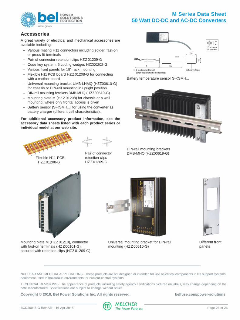
AccessoriesA great variety of electrical and mechanical accessories areavailable including:
– Various mating H11 connectors including solder, fast-on,or press-fit terminals
– Pair of connector retention clips HZZ01209-G– Code key system: 5 coding wedges HZZ00202-G– Various front panels for 19" rack mounting– Flexible H11 PCB board HZZ01208-G for connecting
with a mother board– Universal mounting bracket UMB-LHMQ (HZZ00610-G)
for chassis or DIN-rail mounting in upright position.– DIN-rail mounting brackets DMB-MHQ (HZZ00619-G)– Mounting plate M (HZZ01208) for chassis or a wall
mounting, where only frontal access is given– Battery sensor [S-KSMH...] for using the converter as
battery charger (different cell characteristics).
For additional accessory product information, see theaccessory data sheets listed with each product series orindividual model at our web site.
Flexible H11 PCBHZZ01208-G
Mounting plate M (HZZ01210), connectorwith fast-on terminals (HZZ00101-G),secured with retention clips (HZZ01209-G)
Universal mounting bracket for DIN-railmounting (HZZ00610-G)
Pair of connectorretention clipsHZZ01209-G
EuropeanProjection
Different frontpanels
Battery temperature sensor S-KSMH...
65l
l: 2 m standard length
other cable lengths on request
adhesive tape
30
15
09125
DIN-rail mounting bracketsDMB-MHQ (HZZ00619-G)
NUCLEAR AND MEDICAL APPLICATIONS - These products are not designed or intended for use as critical components in life support systems,equipment used in hazardous environments, or nuclear control systems.
TECHNICAL REVISIONS - The appearance of products, including safety agency certifications pictured on labels, may change depending on thedate manufactured. Specifications are subject to change without notice.