19
https://www.byteparadigm.com/applications/introduction-to-i2c-and-spi-protocols/ M14 – I2C communication protocol
https://www.byteparadigm.com/applications/introduction-to-i2c-and-spi-protocols/
M14 – I2C communication protocol
I²C
I²C is a multi-master protocol that uses 2 signal lines. The two I²C signals are called ‘serial data’ (SDA) and ‘serial clock’ (SCL). There is no need of chip select (slave select) or arbitration logic. Virtually any number of slaves and any number of masters can be connected onto these 2 signal lines and communicate between each other using a protocol that defines:
– 7-bits slave addresses: each device connected to the bus has got such a unique address;
– data divided into 8-bit bytes
– a few control bits for controlling the communication start, end, direction and for an acknowledgment mechanism.
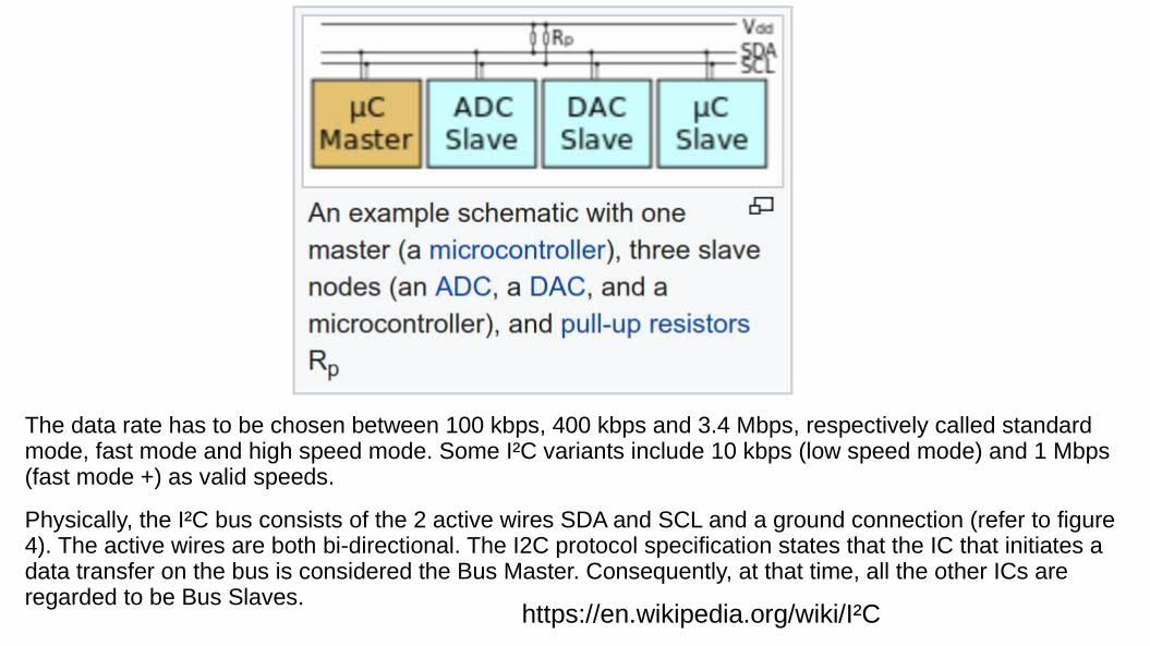
The data rate has to be chosen between 100 kbps, 400 kbps and 3.4 Mbps, respectively called standard mode, fast mode and high speed mode. Some I²C variants include 10 kbps (low speed mode) and 1 Mbps (fast mode +) as valid speeds.
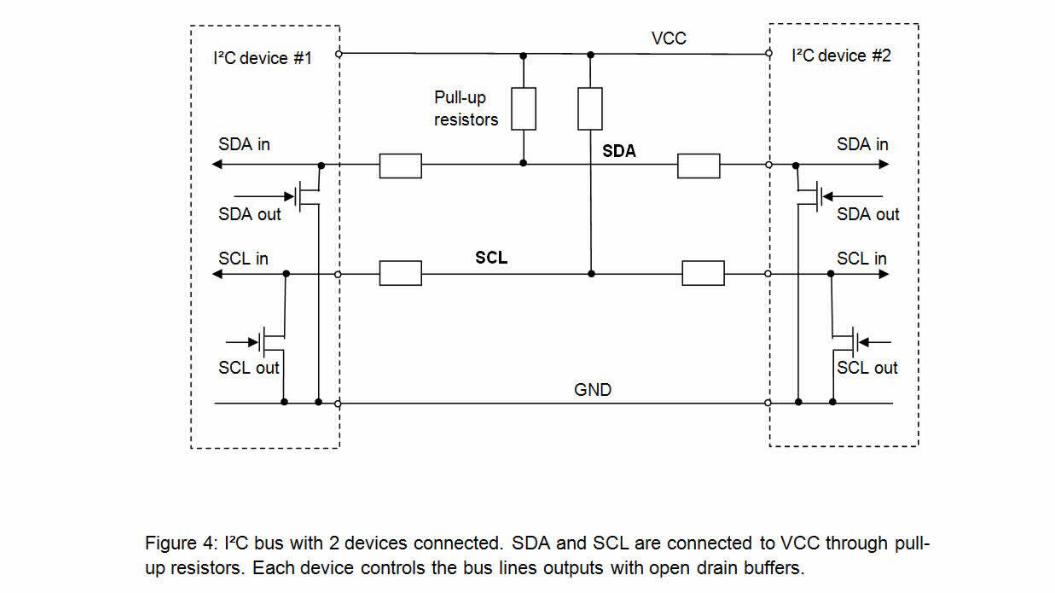
Physically, the I²C bus consists of the 2 active wires SDA and SCL and a ground connection (refer to figure 4). The active wires are both bi-directional. The I2C protocol specification states that the IC that initiates a data transfer on the bus is considered the Bus Master. Consequently, at that time, all the other ICs are regarded to be Bus Slaves.
https://en.wikipedia.org/wiki/I²C
A particular strength of I²C is the capability of a microcontroller to control a network of device chipswith just two general-purpose I/O pins and software
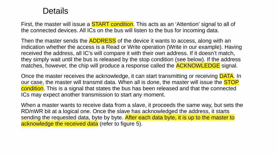
First, the master will issue a START condition. This acts as an ‘Attention’ signal to all of the connected devices. All ICs on the bus will listen to the bus for incoming data.
Then the master sends the ADDRESS of the device it wants to access, along with an indication whether the access is a Read or Write operation (Write in our example). Having received the address, all IC’s will compare it with their own address. If it doesn’t match, they simply wait until the bus is released by the stop condition (see below). If the address matches, however, the chip will produce a response called the ACKNOWLEDGE signal.
Once the master receives the acknowledge, it can start transmitting or receiving DATA. In our case, the master will transmit data. When all is done, the master will issue the STOP condition. This is a signal that states the bus has been released and that the connected ICs may expect another transmission to start any moment.
When a master wants to receive data from a slave, it proceeds the same way, but sets the RD/nWR bit at a logical one. Once the slave has acknowledged the address, it starts sending the requested data, byte by byte. After each data byte, it is up to the master to acknowledge the received data (refer to figure 5).
Details
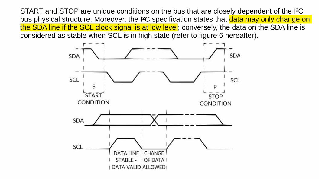
START and STOP are unique conditions on the bus that are closely dependent of the I²Cbus physical structure. Moreover, the I²C specification states that data may only change on the SDA line if the SCL clock signal is at low level; conversely, the data on the SDA line is considered as stable when SCL is in high state (refer to figure 6 hereafter).
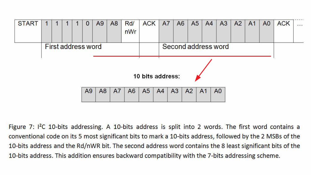
– Expansion to 10-bits device addressing
Any I²C device must have a built-in 7 bits address. In theory, this means that there would be only 128 different I²C devices types in the world. Practically, there are much more different I²C devices and it is a high probability that 2 devices have the same address on a I²C bus. To overcome this limitation, devices often have multiple built-in addresses that the engineer can chose through external configuration pins on the device. The I²C specification also foresees a 10-bits addressing scheme in order to extend the range of available devices address.
Practically, this has got the following impact on the I²C protocol (refer to figure 7):
– Two address words are used for device addressing instead of one.
– The first address word MSBs are conventionally coded as “11110” so any device on the bus is aware the master sends a 10 bits device address.
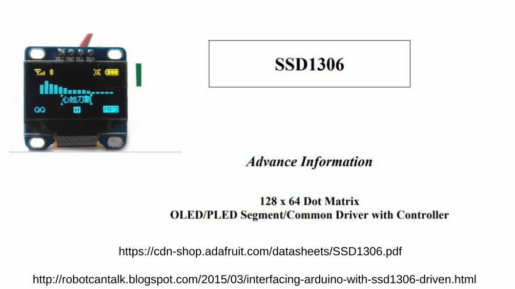
https://cdn-shop.adafruit.com/datasheets/SSD1306.pdf
http://robotcantalk.blogspot.com/2015/03/interfacing-arduino-with-ssd1306-driven.html
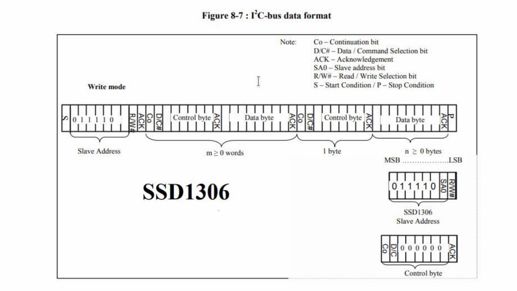
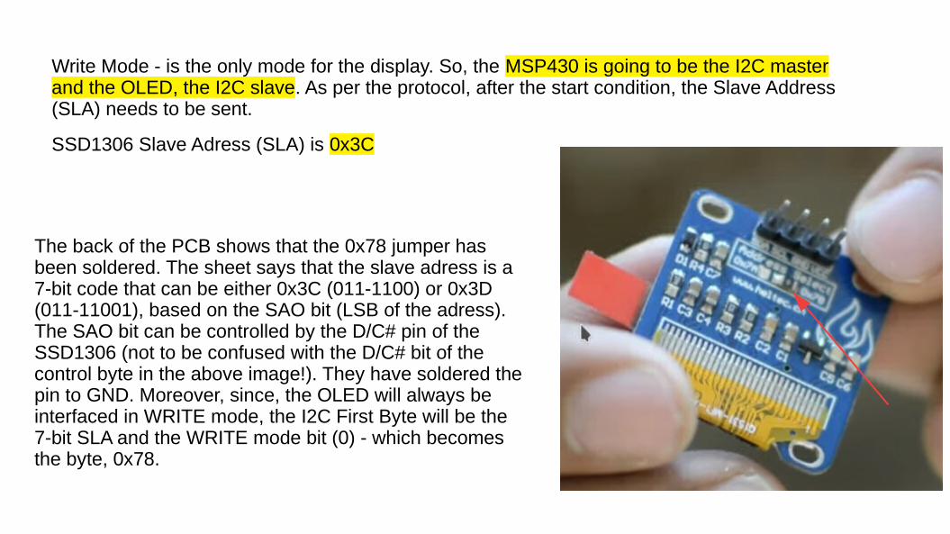
Write Mode - is the only mode for the display. So, the MSP430 is going to be the I2C master and the OLED, the I2C slave. As per the protocol, after the start condition, the Slave Address (SLA) needs to be sent.
SSD1306 Slave Adress (SLA) is 0x3C
The back of the PCB shows that the 0x78 jumper has been soldered. The sheet says that the slave adress is a 7-bit code that can be either 0x3C (011-1100) or 0x3D (011-11001), based on the SAO bit (LSB of the adress). The SAO bit can be controlled by the D/C# pin of the SSD1306 (not to be confused with the D/C# bit of the control byte in the above image!). They have soldered the pin to GND. Moreover, since, the OLED will always be interfaced in WRITE mode, the I2C First Byte will be the 7-bit SLA and the WRITE mode bit (0) - which becomes the byte, 0x78.
http://www.diymalls.com/OLED/0.96-blue-and-yellow-oled-display
Document link: http://www.diymalls.com/files/IIC_OLED.zip user name and password is diymall
For 0.96 inch: 0.96 inch use SSD1306 drive chip. Copy "Adafruit_SSD1306.h" and"Adafruit_GFX.h" into "x:\arduino-1.X.X\libraries".
In order to reduce the pins’ number, we use a hardware RESET system. So thestandard library form Adafruit or u8glib may not very suitable. Make sure you areusing our provided libraries, It’s very important. If those files already in youlibraries, replace it.
https://libraries.io/github/adafruit/Adafruit-GFX-Library
You can download our SSD1306 OLED display Arduino library from github which comes with example code. The library can print text, bitmaps, pixels, rectangles, circles and lines. It uses 1K of RAM since it needs to buffer the entire display but its very fast! The code is simple to adapt to any other microcontrolle
The drivers for these two displays are very different. The monochrome SSD1306 does not have direct access to the display memory, so we have to write to an in-memory frame-buffer, then use that to refresh the screen. Clearing the display is as simple as doing a memset on the entire frame buffer in SRAM - but that only clears the frame buffer. You need to call display() to actually upload the cleared buffer to the display.
So the problem now is the Adafruit_SSD1306 library with its heavy SRAM use of 1KB for the display buffer.
https://www.best-microcontroller-projects.com/ssd1306.html
https://github.com/olikraus/u8g2/wiki/u8g2reference
Examples:
M14 – Example 1 – just light up the display – Initialization details
M14 – Example 2 – alternating test patterns
M14 – Example 3 – Grove graphics test demo
M14 – Example 4 – oledApp test demo
These programs show the complicated initialization command sequencerequired by the SSD 1306 and OLED
They also show code segments that are examples which can be used inapplication programs
Examples 1 & 2 talk directly through the USCB0 software, 3 & 4 use theEnergia Wire library - YMMV


