20
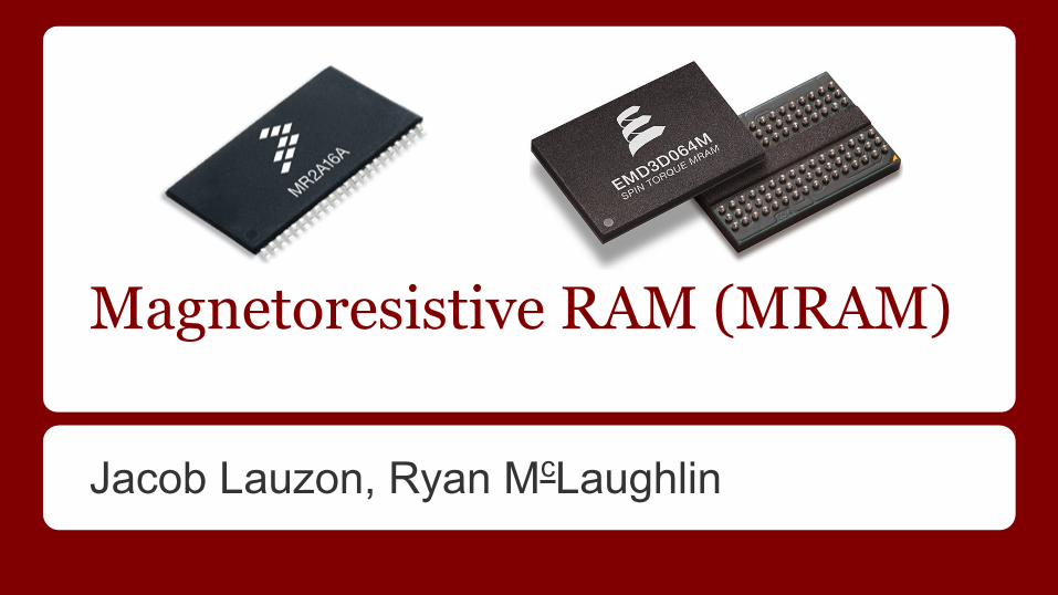
Magnetoresistive RAM (MRAM) Jacob Lauzon, Ryan M c Laughlin
| Date post: | 14-Mar-2018 |
| Category: |
Documents |
| Upload: | truongxuyen |
| View: | 220 times |
| Download: | 2 times |
Magnetoresistive RAM (MRAM)
Jacob Lauzon, Ryan McLaughlin

Agenda
● Current solutions● Why MRAM?● What is MRAM?● History● How it works● Comparisons● Outlook
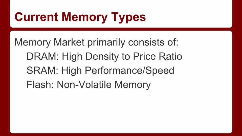
Current Memory Types
Memory Market primarily consists of:DRAM: High Density to Price RatioSRAM: High Performance/SpeedFlash: Non-Volatile Memory
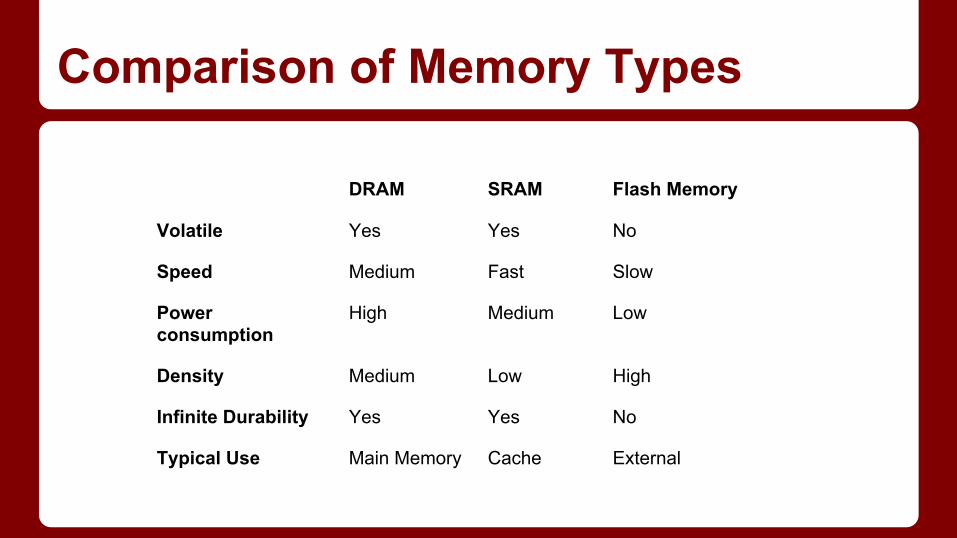
Comparison of Memory Types
DRAM SRAM Flash Memory
Volatile Yes Yes No
Speed Medium Fast Slow
Power consumption
High Medium Low
Density Medium Low High
Infinite Durability Yes Yes No
Typical Use Main Memory Cache External

Why do we need MRAM?
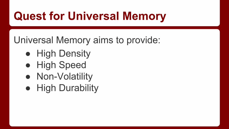
Quest for Universal Memory
Universal Memory aims to provide:● High Density● High Speed● Non-Volatility● High Durability
Non-volatile random access memory Stores data using magnetic charge rather than electrical chargeVery high speed (SRAM speed) with high density (DRAM density)Low power consumption (30% of DRAM)Key Players: Everspin(Motorola/Freescale), Canon, Crocus, Cypress, IBM, Intel, Infineon
What is MRAM?
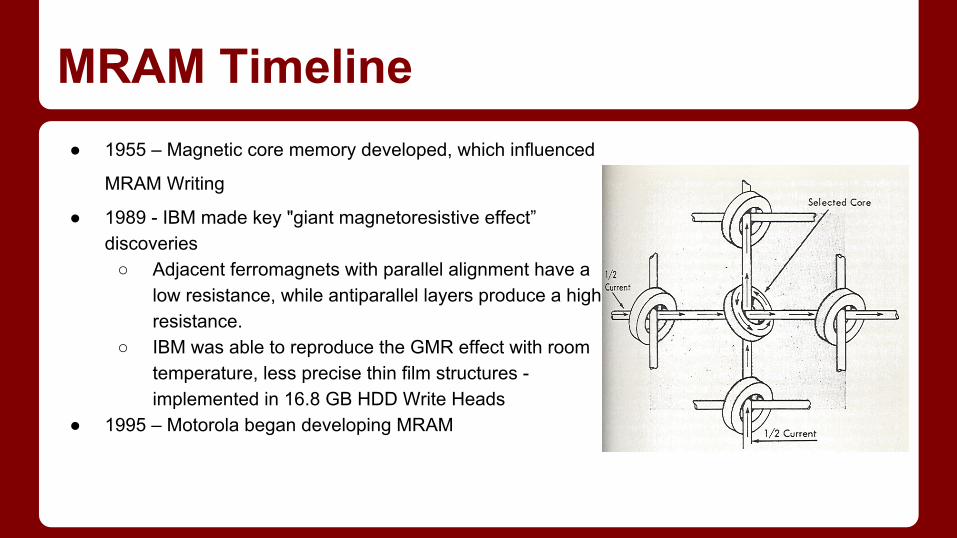
MRAM Timeline● 1955 – Magnetic core memory developed, which influenced
MRAM Writing
● 1989 - IBM made key "giant magnetoresistive effect” discoveries
○ Adjacent ferromagnets with parallel alignment have a low resistance, while antiparallel layers produce a high resistance.
○ IBM was able to reproduce the GMR effect with room temperature, less precise thin film structures - implemented in 16.8 GB HDD Write Heads
● 1995 – Motorola began developing MRAM
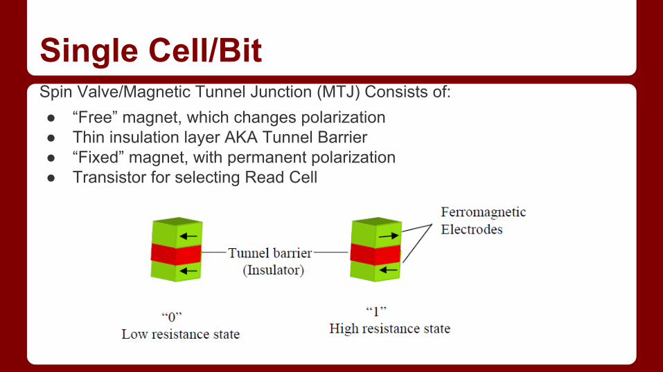
Single Cell/BitSpin Valve/Magnetic Tunnel Junction (MTJ) Consists of:● “Free” magnet, which changes polarization● Thin insulation layer AKA Tunnel Barrier● “Fixed” magnet, with permanent polarization● Transistor for selecting Read Cell
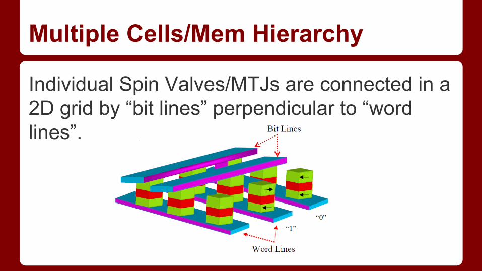
Multiple Cells/Mem Hierarchy
Individual Spin Valves/MTJs are connected in a 2D grid by “bit lines” perpendicular to “word lines”.
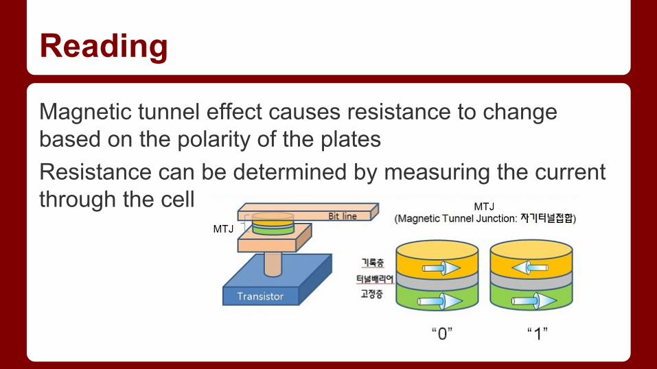
Reading
Magnetic tunnel effect causes resistance to change based on the polarity of the platesResistance can be determined by measuring the current through the cell
Write Methods: Toggle
Decoders are used to power the appropriate bit line and word line for the write.This induces a magnetic field at the junction of the two lines which the free magnet picks upThe direction of the current will determine polarizationDisadvantages:● High current required to induce the field● Size limitation: Cells need to be spread out to avoid the the induced
field overlapping into other cells
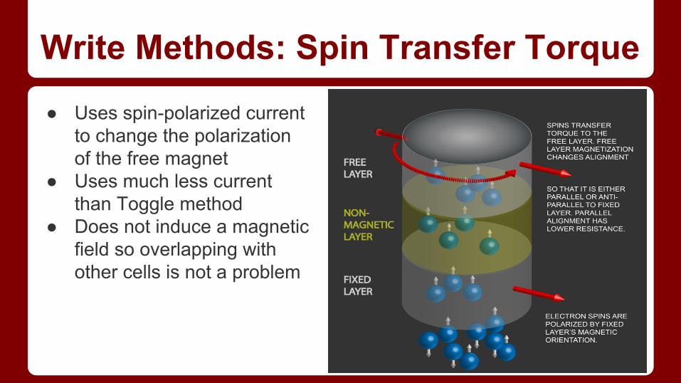
Write Methods: Spin Transfer Torque
● Uses spin-polarized current to change the polarization of the free magnet
● Uses much less current than Toggle method
● Does not induce a magnetic field so overlapping with other cells is not a problem

Write Methods: Others
Thermal-Assisted Switching (TAS) - Uses toggle method but heats up the junction during a write to reduce the field neededVertical-Transport (V) - Sends current through a vertical column to change the polarity. The direction of the current determines the polarity
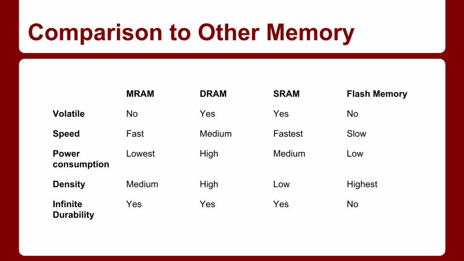
Comparison to Other Memory
MRAM DRAM SRAM Flash Memory
Volatile No Yes Yes No
Speed Fast Medium Fastest Slow
Power consumption
Lowest High Medium Low
Density Medium High Low Highest
Infinite Durability
Yes Yes Yes No
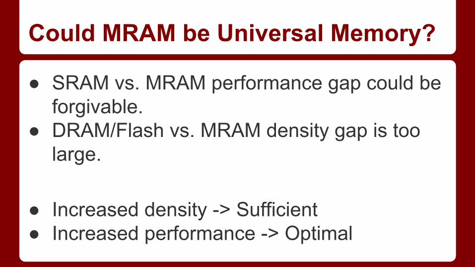
Could MRAM be Universal Memory?
● SRAM vs. MRAM performance gap could be forgivable.
● DRAM/Flash vs. MRAM density gap is too large.
● Increased density -> Sufficient● Increased performance -> Optimal
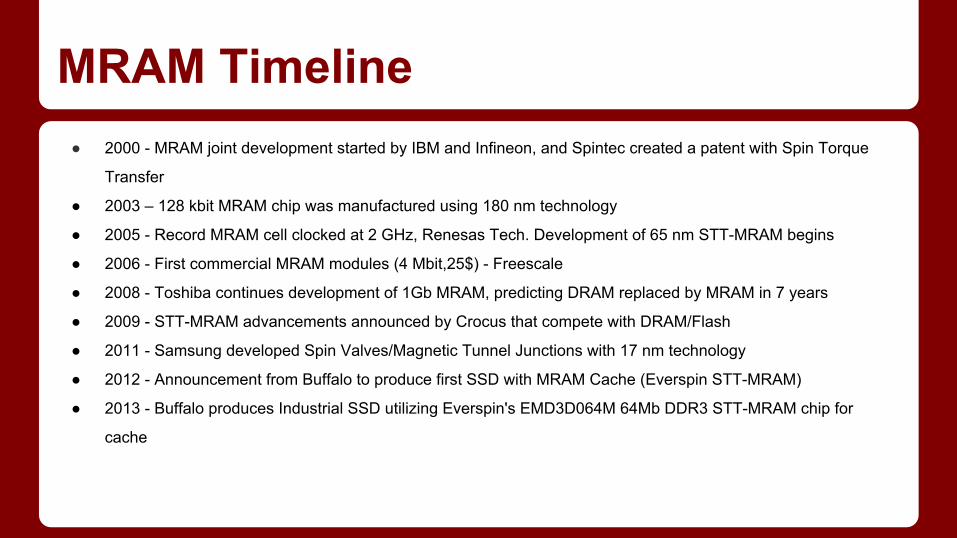
MRAM Timeline● 2000 - MRAM joint development started by IBM and Infineon, and Spintec created a patent with Spin Torque
Transfer
● 2003 – 128 kbit MRAM chip was manufactured using 180 nm technology
● 2005 - Record MRAM cell clocked at 2 GHz, Renesas Tech. Development of 65 nm STT-MRAM begins
● 2006 - First commercial MRAM modules (4 Mbit,25$) - Freescale
● 2008 - Toshiba continues development of 1Gb MRAM, predicting DRAM replaced by MRAM in 7 years
● 2009 - STT-MRAM advancements announced by Crocus that compete with DRAM/Flash
● 2011 - Samsung developed Spin Valves/Magnetic Tunnel Junctions with 17 nm technology
● 2012 - Announcement from Buffalo to produce first SSD with MRAM Cache (Everspin STT-MRAM)
● 2013 - Buffalo produces Industrial SSD utilizing Everspin's EMD3D064M 64Mb DDR3 STT-MRAM chip for
cache
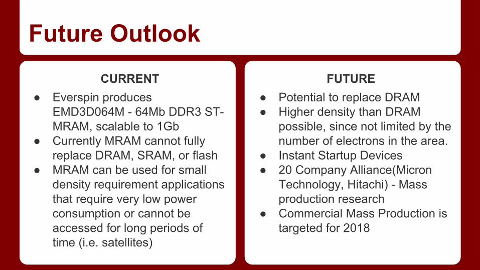
Future OutlookCURRENT
● Everspin produces EMD3D064M - 64Mb DDR3 ST-MRAM, scalable to 1Gb
● Currently MRAM cannot fully replace DRAM, SRAM, or flash
● MRAM can be used for small density requirement applications that require very low power consumption or cannot be accessed for long periods of time (i.e. satellites)
FUTURE● Potential to replace DRAM● Higher density than DRAM
possible, since not limited by the number of electrons in the area.
● Instant Startup Devices● 20 Company Alliance(Micron
Technology, Hitachi) - Mass production research
● Commercial Mass Production is targeted for 2018

Questions?
Bibliography● http://en.kisti.re.kr/blog/post/scientists-find-solution-preventing-malfunction-next-generation-magnetic-memory/● http://www.intechopen.com/books/electronic-properties-of-carbon-nanotubes/carbon-nanotube-based-magnetic-
tunnel-junctions-mtjs-for-spintronics-application#F6● http://en.wikipedia.org/wiki/Mram● http://nram.com/pdf/Nantero_Memory.pdf● http://www.eejournal.com/archives/articles/20130107-mram/● http://www.blogcdn.com/www.engadget.com/media/2012/11/everspin-11-14-12-02.jpg● http://www.electronicproducts.com/images2/F101FREE0107.gif● http://www.columbia.edu/cu/computinghistory/core.jpg● http://www.research.ibm.com/research/gmr.html● http://asia.nikkei.com/Business/Companies/DRAMs-days-numbered-as-Japan-US-chip-alliance-homes-in-on-
MRAM


