(Reprinted with permission from IOP Publishing Ltd.,And courtesy of Professor Anja Boisen)
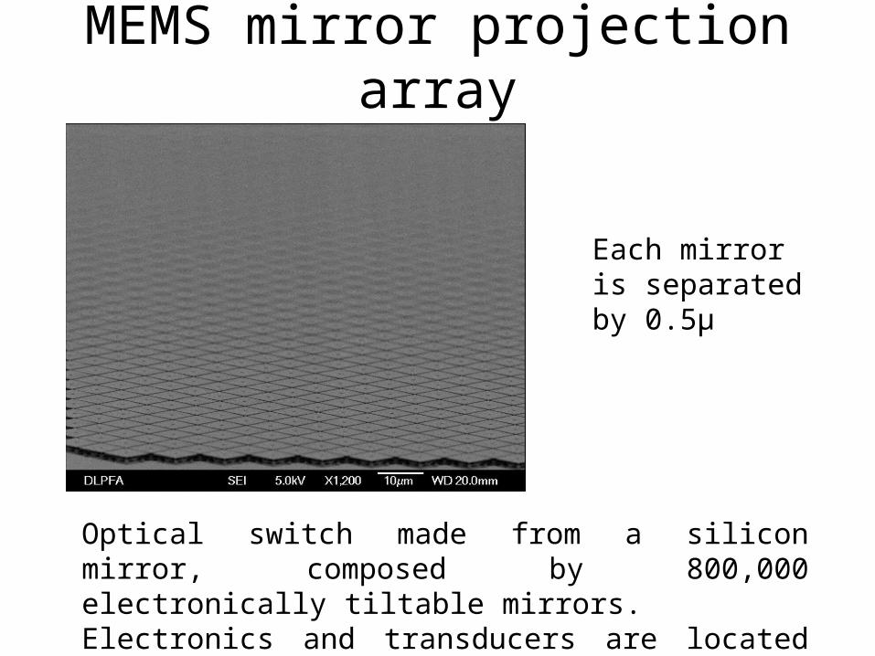
MEMS mirror projection array
Optical switch made from a silicon mirror, composed by 800,000 electronically tiltable mirrors. Electronics and transducers are located under each mirror.
Each mirror is separated by 0.5μ
Thin Film TechnologiesThin Film Technologies
• From the kinetic theory of gases:
M
Tv 42 1058.1 RMS speed in cm/s from the
equipartition theorem
2
32
1vN s
For O2 at 300K this is ca. 1015 molecules·cm-2 at 10-6 Torr:
≈ a monolayer of adsorbed molecule per second.
A vacuum of 10-9 torr is required.
Number of molecules hitting a surface per unit time
Modes of epitaxial growthModes of epitaxial growth
Epitaxial growthEpitaxial growth: in a homogeneous system, element x is deposited onto a surface of a single crystal of the same element.
Layer-by-layer uniform growth
2D-growth favourite with respect to 3D-growth.
3D-growth favourite with respect to 2D-growth.
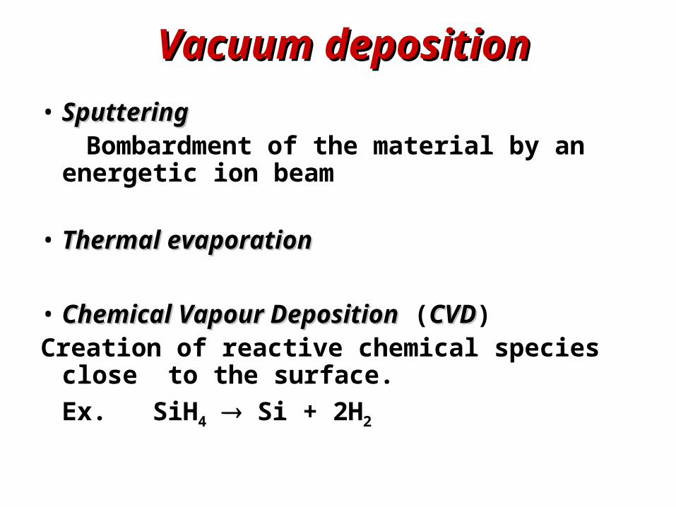
Vacuum depositionVacuum deposition
• SputteringSputtering Bombardment of the material by an energetic ion
beam
• Thermal evaporationThermal evaporation
• Chemical Vapour DepositionChemical Vapour Deposition (CVDCVD) Creation of reactive chemical species close to the
surface.
Ex. SiH4 Si + 2H2
UHV Thin Film Deposition SystemUHV Thin Film Deposition System
(Courtesy of Professor Robert Lad, Laboratory for Surface Science and Technology, University of Maine)
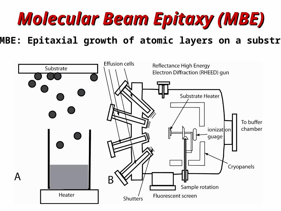
Molecular Beam Epitaxy (MBE)Molecular Beam Epitaxy (MBE)MBE: Epitaxial growth of atomic layers on a substrate
Strain energy limits thickness Kinetic factors
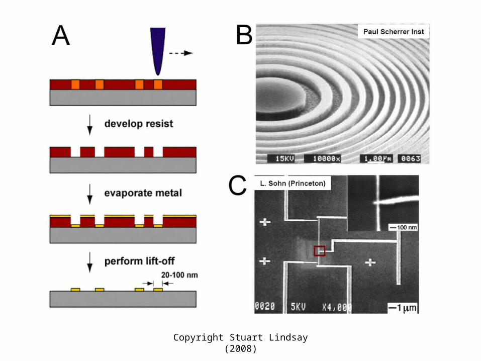
Copyright Stuart Lindsay (2008)
(Courtesy of Professor Jeff Drucker, Department and School of Materials, Arizona State University)
• trapping of adatoms at special sites• diffusion on the surface• association/dissociation rate of small clusters• formation rate of stable clusters
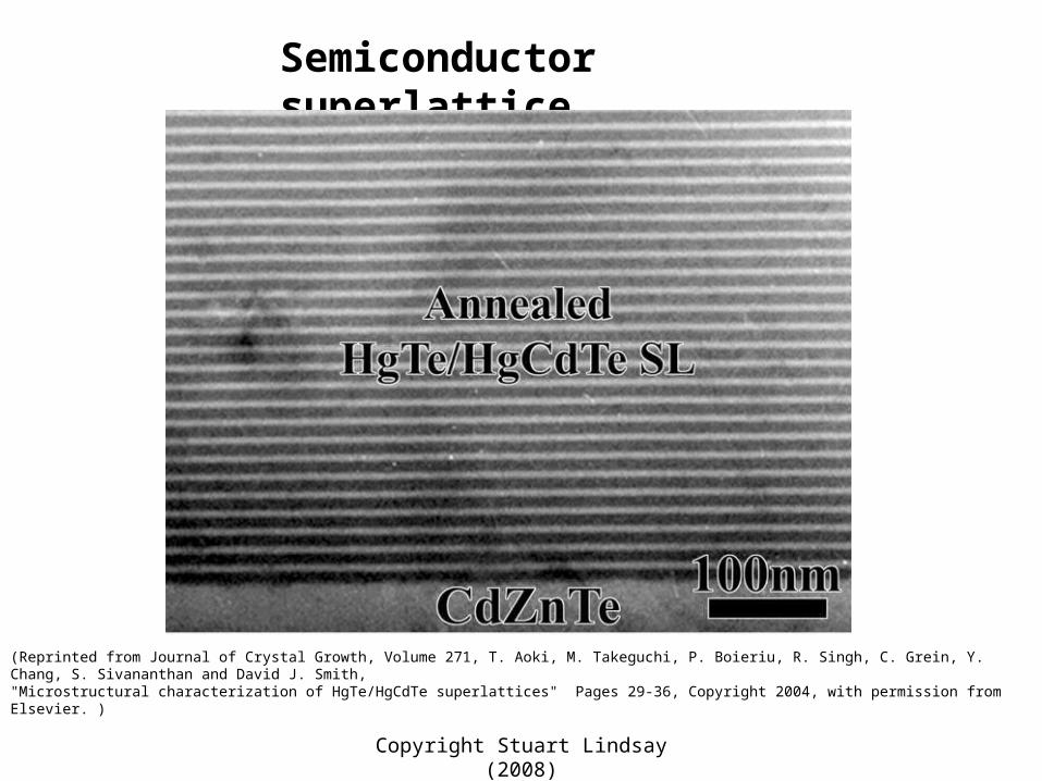
Semiconductor superlattice
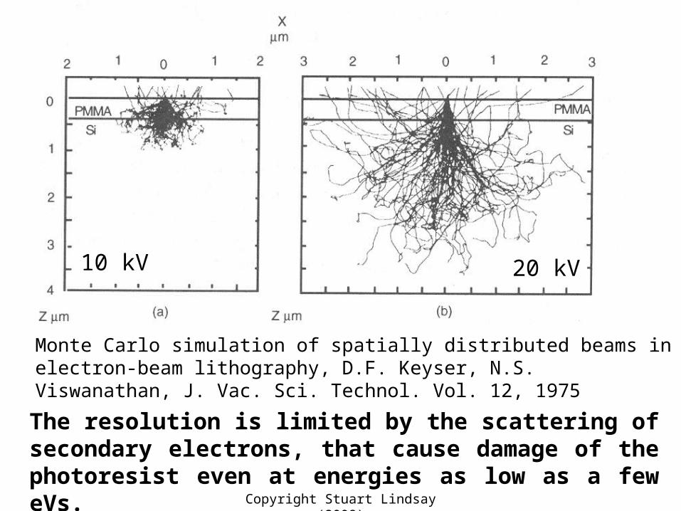
Copyright Stuart Lindsay (2008)
(Reprinted from Journal of Crystal Growth, Volume 271, T. Aoki, M. Takeguchi, P. Boieriu, R. Singh, C. Grein, Y. Chang, S. Sivananthan and David J. Smith, "Microstructural characterization of HgTe/HgCdTe superlattices" Pages 29-36, Copyright 2004, with permission from Elsevier. )
Immiscible polymers phase-separate into a quite ordered domain structure
Copyright Stuart Lindsay (2008)
Self-assembled masksSelf-assembled masks
Polystyrene/polybutadiene 36/11
Spontaneously forms nanometer scale phase-separated domains.
Polybutadiene is selectively etched by ozone treatment.
Structures made with block-copolymer masksStructures made with block-copolymer masks
TEM images showing (A) a spherical micro-domain monolayer film after removal of poly butadiene by ozone treatment, (B) the resulting array of holes in silicon nitride after RIE, (C) cylindrical microdomains in which the darker regions are osmium stained poly butadiene domains and (D) the resulting cylindrical pattern etched into the silicon nitride surface.
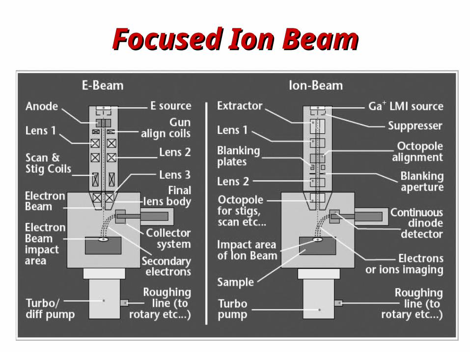
Focused Ion BeamFocused Ion Beam
Focused Ion BeamFocused Ion Beam
Gallium liquid metal ion source. Typical energies of ion beams are 5-30 kV.
Copyright Stuart Lindsay (2008)
• collection of the scattered ions (ion beam imaging)
• collection of secondary electrons
• implantation of Gallium ions
Ions are thousands of times heavier than electrons:Electrostatic fields are more efficient than magnetic fields(electrostatic focusing)
Focused Ion BeamFocused Ion Beam
Resolution: few tens of nanometers
Ion beam irradiation of a gold film
SEM image of an insulator defect.The sample was prepared by a FIB.
Stamp TechnologyStamp Technology
Chemical patterning by soft imprint lithography.
Thermoplastic
““Stamped” MOSFET with 60nm gateStamped” MOSFET with 60nm gate
Fabrication of 60 nm transistors on 4-in wager using nanoimprint at all lithography levels
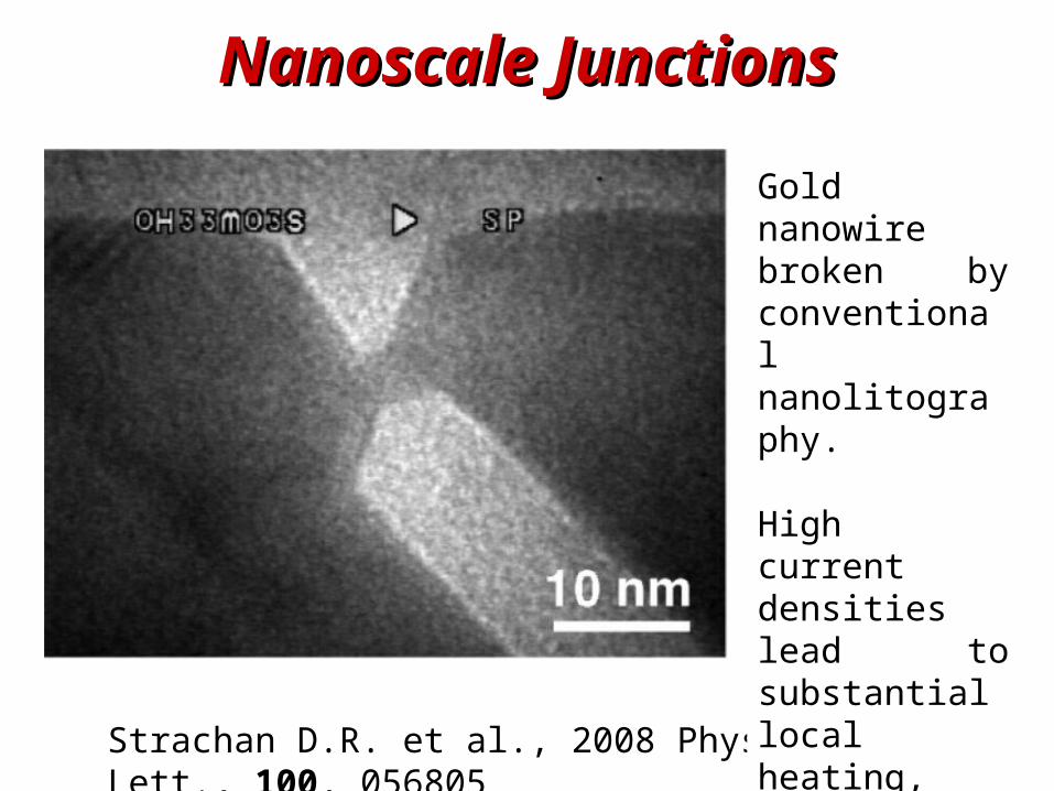
Nanoscale JunctionsNanoscale Junctions
Strachan D.R. et al., 2008 Phys. Rev. Lett., 100, 056805
Gold nanowire broken by conventional nanolitography.
High current densities lead to substantial local heating, causing electromigration.