97
User Manual MV-D1024E-3D01-160 3D CMOS Camera MAN037 04/2009 V1.1
| Date post: | 17-Mar-2016 |
| Category: |
Documents |
| Upload: | emi-eguchi |
| View: | 225 times |
| Download: | 0 times |

User Manual
MV-D1024E-3D01-1603D CMOS Camera
MAN037 04/2009 V1.1


All information provided in this manual is believed to be accurate and reliable. Noresponsibility is assumed by Photonfocus AG for its use. Photonfocus AG reserves the right tomake changes to this information without notice.Reproduction of this manual in whole or in part, by any means, is prohibited without priorpermission having been obtained from Photonfocus AG.
1

2
Contents
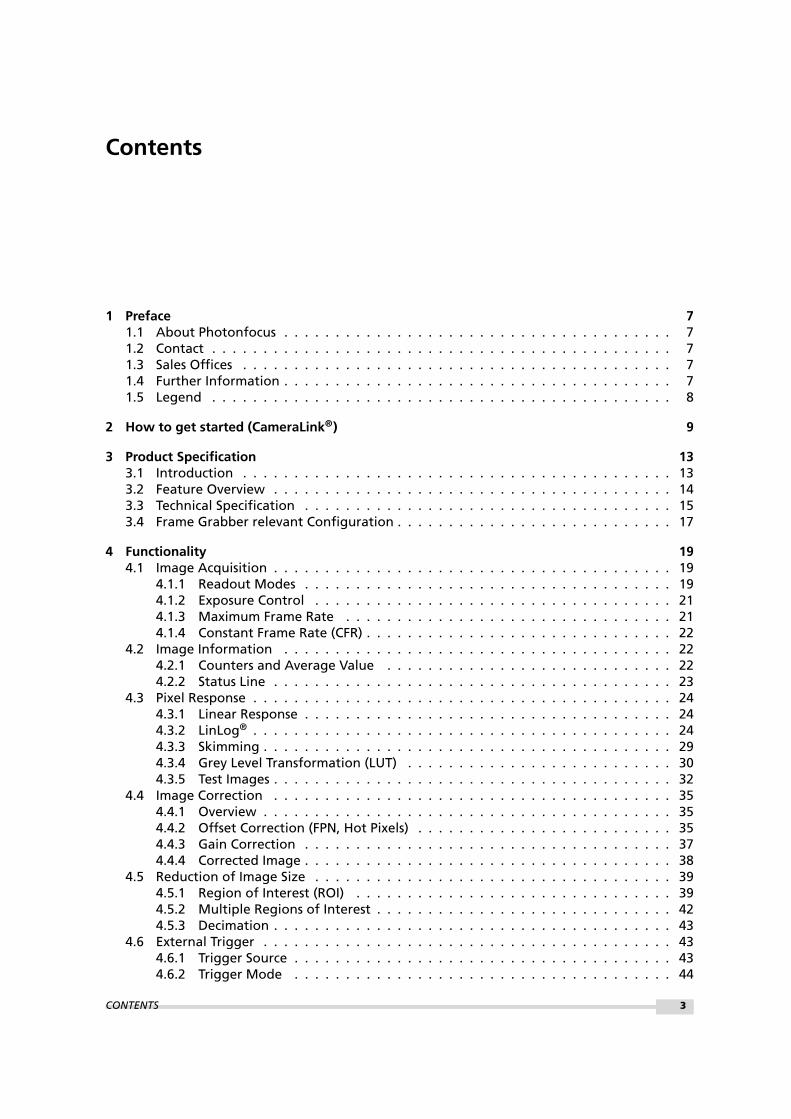
1 Preface 71.1 About Photonfocus . . . . . . . . . . . . . . . . . . . . . . . . . . . . . . . . . . . . . . 71.2 Contact . . . . . . . . . . . . . . . . . . . . . . . . . . . . . . . . . . . . . . . . . . . . . 71.3 Sales Offices . . . . . . . . . . . . . . . . . . . . . . . . . . . . . . . . . . . . . . . . . . 71.4 Further Information . . . . . . . . . . . . . . . . . . . . . . . . . . . . . . . . . . . . . . 71.5 Legend . . . . . . . . . . . . . . . . . . . . . . . . . . . . . . . . . . . . . . . . . . . . . 8
2 How to get started (CameraLink®) 9
3 Product Specification 133.1 Introduction . . . . . . . . . . . . . . . . . . . . . . . . . . . . . . . . . . . . . . . . . . 133.2 Feature Overview . . . . . . . . . . . . . . . . . . . . . . . . . . . . . . . . . . . . . . . 143.3 Technical Specification . . . . . . . . . . . . . . . . . . . . . . . . . . . . . . . . . . . . 153.4 Frame Grabber relevant Configuration . . . . . . . . . . . . . . . . . . . . . . . . . . . 17
4 Functionality 194.1 Image Acquisition . . . . . . . . . . . . . . . . . . . . . . . . . . . . . . . . . . . . . . . 19
4.1.1 Readout Modes . . . . . . . . . . . . . . . . . . . . . . . . . . . . . . . . . . . . 194.1.2 Exposure Control . . . . . . . . . . . . . . . . . . . . . . . . . . . . . . . . . . . 214.1.3 Maximum Frame Rate . . . . . . . . . . . . . . . . . . . . . . . . . . . . . . . . 214.1.4 Constant Frame Rate (CFR) . . . . . . . . . . . . . . . . . . . . . . . . . . . . . . 22
4.2 Image Information . . . . . . . . . . . . . . . . . . . . . . . . . . . . . . . . . . . . . . 224.2.1 Counters and Average Value . . . . . . . . . . . . . . . . . . . . . . . . . . . . 224.2.2 Status Line . . . . . . . . . . . . . . . . . . . . . . . . . . . . . . . . . . . . . . . 23
4.3 Pixel Response . . . . . . . . . . . . . . . . . . . . . . . . . . . . . . . . . . . . . . . . . 244.3.1 Linear Response . . . . . . . . . . . . . . . . . . . . . . . . . . . . . . . . . . . . 244.3.2 LinLog® . . . . . . . . . . . . . . . . . . . . . . . . . . . . . . . . . . . . . . . . . 244.3.3 Skimming . . . . . . . . . . . . . . . . . . . . . . . . . . . . . . . . . . . . . . . . 294.3.4 Grey Level Transformation (LUT) . . . . . . . . . . . . . . . . . . . . . . . . . . 304.3.5 Test Images . . . . . . . . . . . . . . . . . . . . . . . . . . . . . . . . . . . . . . . 32
4.4 Image Correction . . . . . . . . . . . . . . . . . . . . . . . . . . . . . . . . . . . . . . . 354.4.1 Overview . . . . . . . . . . . . . . . . . . . . . . . . . . . . . . . . . . . . . . . . 354.4.2 Offset Correction (FPN, Hot Pixels) . . . . . . . . . . . . . . . . . . . . . . . . . 354.4.3 Gain Correction . . . . . . . . . . . . . . . . . . . . . . . . . . . . . . . . . . . . 374.4.4 Corrected Image . . . . . . . . . . . . . . . . . . . . . . . . . . . . . . . . . . . . 38
4.5 Reduction of Image Size . . . . . . . . . . . . . . . . . . . . . . . . . . . . . . . . . . . 394.5.1 Region of Interest (ROI) . . . . . . . . . . . . . . . . . . . . . . . . . . . . . . . 394.5.2 Multiple Regions of Interest . . . . . . . . . . . . . . . . . . . . . . . . . . . . . 424.5.3 Decimation . . . . . . . . . . . . . . . . . . . . . . . . . . . . . . . . . . . . . . . 43
4.6 External Trigger . . . . . . . . . . . . . . . . . . . . . . . . . . . . . . . . . . . . . . . . 434.6.1 Trigger Source . . . . . . . . . . . . . . . . . . . . . . . . . . . . . . . . . . . . . 434.6.2 Trigger Mode . . . . . . . . . . . . . . . . . . . . . . . . . . . . . . . . . . . . . 44
CONTENTS 3

CONTENTS
4.6.3 Trigger Delay . . . . . . . . . . . . . . . . . . . . . . . . . . . . . . . . . . . . . . 444.6.4 Trigger Resolution . . . . . . . . . . . . . . . . . . . . . . . . . . . . . . . . . . . 45
4.7 Strobe Output . . . . . . . . . . . . . . . . . . . . . . . . . . . . . . . . . . . . . . . . . 454.8 Additional 3D Functionality . . . . . . . . . . . . . . . . . . . . . . . . . . . . . . . . . 46
4.8.1 Mode Settings . . . . . . . . . . . . . . . . . . . . . . . . . . . . . . . . . . . . . 464.8.2 Threshold . . . . . . . . . . . . . . . . . . . . . . . . . . . . . . . . . . . . . . . . 464.8.3 Insertion of 3D Data . . . . . . . . . . . . . . . . . . . . . . . . . . . . . . . . . 474.8.4 Interpolation Technique . . . . . . . . . . . . . . . . . . . . . . . . . . . . . . . 48
4.9 Configuration Interface (CameraLink) . . . . . . . . . . . . . . . . . . . . . . . . . . . 50
5 Hardware Interface 515.1 Connectors . . . . . . . . . . . . . . . . . . . . . . . . . . . . . . . . . . . . . . . . . . . 51
5.1.1 CameraLink Connector for CameraLink Camera Models . . . . . . . . . . . . . 515.1.2 Power Supply for CameraLink Camera Models . . . . . . . . . . . . . . . . . . 515.1.3 Trigger and Strobe Signals . . . . . . . . . . . . . . . . . . . . . . . . . . . . . . 525.1.4 Status Indicator (CameraLink Cameras) . . . . . . . . . . . . . . . . . . . . . . 53
5.2 CameraLink Data Interface . . . . . . . . . . . . . . . . . . . . . . . . . . . . . . . . . . 535.3 Read-out Timing . . . . . . . . . . . . . . . . . . . . . . . . . . . . . . . . . . . . . . . . 56
5.3.1 Free running Mode . . . . . . . . . . . . . . . . . . . . . . . . . . . . . . . . . . 565.3.2 Constant Frame Rate Mode (CFR) . . . . . . . . . . . . . . . . . . . . . . . . . . 58
5.4 Trigger . . . . . . . . . . . . . . . . . . . . . . . . . . . . . . . . . . . . . . . . . . . . . 605.4.1 Trigger Modes . . . . . . . . . . . . . . . . . . . . . . . . . . . . . . . . . . . . . 605.4.2 Trigger Delay . . . . . . . . . . . . . . . . . . . . . . . . . . . . . . . . . . . . . . 62
6 The PFRemote Control Tool 656.1 Overview . . . . . . . . . . . . . . . . . . . . . . . . . . . . . . . . . . . . . . . . . . . . 656.2 PFRemote and PFLib . . . . . . . . . . . . . . . . . . . . . . . . . . . . . . . . . . . . . 656.3 Operating System . . . . . . . . . . . . . . . . . . . . . . . . . . . . . . . . . . . . . . . 656.4 Installation Notes . . . . . . . . . . . . . . . . . . . . . . . . . . . . . . . . . . . . . . . 656.5 Graphical User Interface (GUI) . . . . . . . . . . . . . . . . . . . . . . . . . . . . . . . . 66
6.5.1 Port Browser . . . . . . . . . . . . . . . . . . . . . . . . . . . . . . . . . . . . . . 666.5.2 Ports, Device Initialization . . . . . . . . . . . . . . . . . . . . . . . . . . . . . . 666.5.3 Main Buttons . . . . . . . . . . . . . . . . . . . . . . . . . . . . . . . . . . . . . 68
6.6 Device Properties . . . . . . . . . . . . . . . . . . . . . . . . . . . . . . . . . . . . . . . 68
7 Graphical User Interface (GUI) 697.1 MV-D1024E-3D01-160 . . . . . . . . . . . . . . . . . . . . . . . . . . . . . . . . . . . . . 69
7.1.1 Exposure . . . . . . . . . . . . . . . . . . . . . . . . . . . . . . . . . . . . . . . . 707.1.2 Window . . . . . . . . . . . . . . . . . . . . . . . . . . . . . . . . . . . . . . . . 717.1.3 Trigger . . . . . . . . . . . . . . . . . . . . . . . . . . . . . . . . . . . . . . . . . 737.1.4 Data Output . . . . . . . . . . . . . . . . . . . . . . . . . . . . . . . . . . . . . . 757.1.5 Characteristics . . . . . . . . . . . . . . . . . . . . . . . . . . . . . . . . . . . . . 777.1.6 3D01 . . . . . . . . . . . . . . . . . . . . . . . . . . . . . . . . . . . . . . . . . . 787.1.7 Correction . . . . . . . . . . . . . . . . . . . . . . . . . . . . . . . . . . . . . . . 797.1.8 Info . . . . . . . . . . . . . . . . . . . . . . . . . . . . . . . . . . . . . . . . . . . 81
8 Mechanical and Optical Considerations 838.1 Mechanical Interface for CameraLink Camera Models . . . . . . . . . . . . . . . . . . 838.2 Optical Interface . . . . . . . . . . . . . . . . . . . . . . . . . . . . . . . . . . . . . . . . 84
8.2.1 Cleaning the Sensor . . . . . . . . . . . . . . . . . . . . . . . . . . . . . . . . . . 848.3 Compliance . . . . . . . . . . . . . . . . . . . . . . . . . . . . . . . . . . . . . . . . . . . 86
4

9 Warranty 879.1 Warranty Terms . . . . . . . . . . . . . . . . . . . . . . . . . . . . . . . . . . . . . . . . 879.2 Warranty Claim . . . . . . . . . . . . . . . . . . . . . . . . . . . . . . . . . . . . . . . . 87
10 References 89
A Pinouts 91A.1 Power Supply for CameraLink Camera Models . . . . . . . . . . . . . . . . . . . . . . 91
A.1.1 Power Supply Connector . . . . . . . . . . . . . . . . . . . . . . . . . . . . . . . 91A.2 CameraLink Connector for CameraLink Camera Models . . . . . . . . . . . . . . . . . 92
B Revision History 95
CONTENTS 5

CONTENTS
6

1Preface
1.1 About Photonfocus
The Swiss company Photonfocus is one of the leading specialists in the development of CMOSimage sensors and corresponding industrial cameras for machine vision, security & surveillanceand automotive markets.Photonfocus is dedicated to making the latest generation of CMOS technology commerciallyavailable. Active Pixel Sensor (APS) and global shutter technologies enable high speed andhigh dynamic range (120 dB) applications, while avoiding disadvantages like image lag,blooming and smear.Photonfocus has proven that the image quality of modern CMOS sensors is now appropriatefor demanding applications. Photonfocus’ product range is complemented by custom designsolutions in the area of camera electronics and CMOS image sensors.Photonfocus is ISO 9001 certified. All products are produced with the latest techniques in orderto ensure the highest degree of quality.
1.2 Contact
Photonfocus AG, Bahnhofplatz 10, CH-8853 Lachen SZ, Switzerland
Sales Phone: +41 55 451 07 45 Email: [email protected]
Support Phone: +41 55 451 01 37 Email: [email protected]
Table 1.1: Photonfocus Contact
1.3 Sales Offices
Photonfocus products are available through an extensive international distribution networkand through our key account managers. Details of the distributor nearest you and contacts toour key account managers can be found at www.photonfocus.com.
1.4 Further Information
For further information on the products, documentation and software updates please see ourweb site www.photonfocus.com or contact our distributors.
Photonfocus reserves the right to make changes to its products and documenta-tion without notice. Photonfocus products are neither intended nor certified foruse in life support systems or in other critical systems. The use of Photonfocusproducts in such applications is prohibited.
Photonfocus® and LinLog® are registered trademarks of Photonfocus AG.CameraLink® is a registered mark of the Automated Imaging Association. Prod-uct and company names mentioned herein are trademarks or trade names oftheir respective companies.
7
1 Preface
Reproduction of this manual in whole or in part, by any means, is prohibitedwithout prior permission having been obtained from Photonfocus AG.
Photonfocus can not be held responsible for any technical or typographical er-rors.
1.5 Legend
In this documentation the reader’s attention is drawn to the following icons:
Important note
Alerts and additional information
Attention, critical warning
. Notification, user guide
8

2How to get started (CameraLink®)
1. Install a suitable frame grabber in your PC.
To find a compliant frame grabber, please see the frame grabber compatibilitylist at www.photonfocus.com.
2. Install the frame grabber software.
.Without installed frame grabber software the camera configuration tool PFRe-mote will not be able to communicate with the camera. Please follow the in-structions of the frame grabber supplier.
3. Remove the camera from its packaging. Please make sure the following items are includedwith your camera:
• Power supply connector (7-pole power plug)
• Camera body cap
If any items are missing or damaged, please contact your dealership.
4. Remove the camera body cap from the camera and mount a suitable lens.
When removing the camera body cap or when changing the lens, the camerashould always be held with the opening facing downwards to prevent dust ordebris falling onto the CMOS sensor.
Figure 2.1: Camera with protective cap and lens.
Do not touch the sensor surface. Protect the image sensor from particles anddirt!
9

2 How to get started (CameraLink®)
The sensor has no cover glass, therefore dust on the sensor surface may resembleto clusters or extended regions of dead pixel.
To choose a lens, see the Lens Finder in the ’Support’ area atwww.photonfocus.com.
5. Connect the camera to the frame grabber with a suitable CameraLink cable (see Fig. 2.2).CameraLink cables can be purchased from Photonfocus directly (www.photonfocus.com).Please note that Photonfocus provides appropriate solutions for your advanced visionapplications.
Figure 2.2: Camera with frame grabber, power supply and cable.
Do not connect or disconnect the CameraLink cable while camera power is on!For more information about CameraLink see Section 4.9.
6. Connect a suitable power supply to the provided 7-pole power plug. For the connectorassembly see Fig. A.1. The pinout of the connector is shown in Appendix A.
Check the correct supply voltage and polarity! Do not exceed the maximumoperating voltage of +12V DC (± 10%).
7. Connect the power supply to the camera (see Fig. 2.2).
. The status LED on the rear of the camera will light red for a short moment, andthen flash green. For more information see Section 5.1.4.
10

8. Download the camera software PFRemote to your computer.
You can find the latest version of PFRemote on the support page atwww.photonfocus.com.
9. Install the camera software PFRemote. Please follow the instructions of the PFRemotesetup wizard.
Figure 2.3: Screen shot PFremote setup wizard
10. Start the camera software PFRemote and choose the communication port.
Figure 2.4: PFRemote start window
11. Check the status LED on the rear of the camera.
. The status LED lights green when an image is being produced, and it is red whenserial communication is active. For more information see Section 5.1.4.
12. You may display images using the software that is provided by the frame grabbermanufacturer.
11

2 How to get started (CameraLink®)
13. The installation procedure and the system configuration of a suitable PCI Expressframegrabber needed to operate the 3D Suite from Photonfocus is covered in separatedocumentations.
You can find more detailled instructions in the application note AN028 "3D Sys-tem Configuration" in the support area at www.photonfocus.com.
12
3Product Specification
3.1 Introduction
The MV-D1024E-3D01-160 is a CMOS camera from Photonfocus optimized in two aspects forlaser triangulation applications. The camera includes an image processing module, that runs analgorithm called Peak Detector. The Peak Detector algorithm is able to compute with sub-pixelaccurracy the peak position of a laser line. Thus, the height profile of an object gets computedwithin the camera, making additional calculations in the PC obsolet.In several applications solved with laser triangulation setups it was shown that the use of theLinLog®response curve leads to better triangulation results, since information is not gettinglost by saturation of the laser line. The triangulation is getting more stable and independent ofthe object surface properties.The camera is built around the monochrome CMOS image sensor A1024B, developed byPhotonfocus. The principal advantages are:
• High reliability of 3D reconstruction, due to the non-linear interpolation technique usedin the peak detection algorithm
• Peak detection with up to 1/64 subpixel accuracy
• Less post-processing necessary for obtaining perfectly smooth surfaces
• Extremely high image contrast achieved by LinLog®technology
• Stabilization of laser triangulation applications independent from object surfaces
• Detection of small features on the inspected parts due to decreased noise sensitivity
• Combined 2D/3D applications can be realized in the 2D/3D mode of the camera
• Global shutter
• Region of interest (ROI) freely selectable in x and y direction
• Stabilization of laser triangulation applications independent from object surfaces
• Detection of small features on the inspected parts due to decreased noise sensitivity
• Several simultaneously selectable read out windows: Multiple region of interest (MultipleROI)
• The camera has a digital CameraLink® interface (CL base configuration)
• Grey level resolution up to 12 bit
• The compact size of only or 55 x 55 x 40 mm3 make the MV-D1024E-3D01-160 camera theperfect solution for applications in which space is at a premium
The basic components for 3D imaging consist of a laser line and a high speed CMOS camera ina triangular arrangement to capture images (profiles) from objects that are moved on aconveyer belt or in a similar setup (see Fig. 3.1).
You can find more information on the basics of laser triangulation and on theprinciples of 3D image acquisition technique in the user manual "PF 3D Suite"available in the support area at www.photonfocus.com.
.
13

3 Product Specification
C o n v e y o r b e l t w i t h o b j e c t s
L a s e r C a m e r a
Figure 3.1: Triangulation principle with objects moved on a conveyor belt
3.2 Feature Overview
The general specification and features of the camera are listed in the following sections. Thedetailed description of the camera features is given in Chapter 4.
MV-D1024E-3D01-160
Interfaces CameraLink base configuration
Camera Control PFRemote (Windows GUI) or programming library
Configuration Interface serial, 9’600 baud or 57.6 kbaud (user selectable)
Trigger Modes Interface Trigger / I/O Trigger
Exposure Time Defined by camera or trigger pulse width
Features 3D Peak Detector
Linear Mode / LinLog®Mode / Skimming
Shading Correction (Offset and Gain)
Grey level resolution 12 bit / 10 bit / 8 bit
Region of Interest (ROI) / Multiple Regions of Interest (MROI)
Look-up table (10 to 8 bit) / Decimation
Trigger input / Strobe output with programmable delay
Test pattern / Image information / Status line
Table 3.1: Feature overview (see Chapter 4 for more information)
.
14
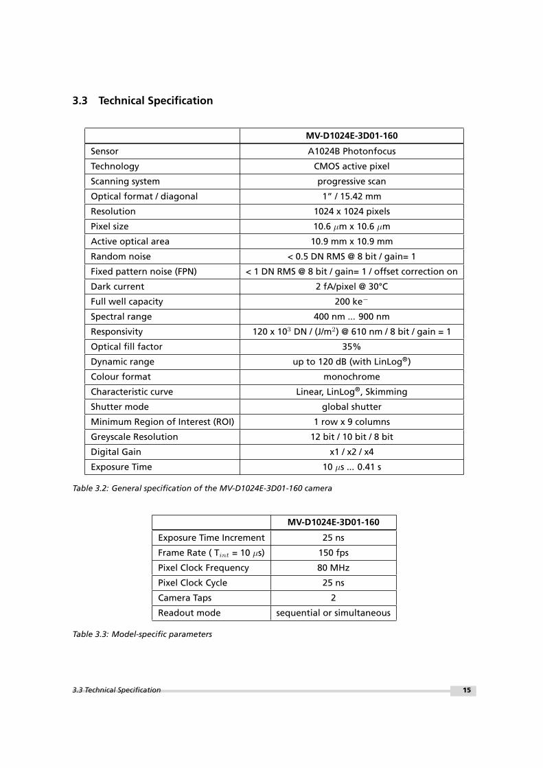
3.3 Technical Specification
MV-D1024E-3D01-160
Sensor A1024B Photonfocus
Technology CMOS active pixel
Scanning system progressive scan
Optical format / diagonal 1” / 15.42 mm
Resolution 1024 x 1024 pixels
Pixel size 10.6 µm x 10.6 µm
Active optical area 10.9 mm x 10.9 mm
Random noise < 0.5 DN RMS @ 8 bit / gain= 1
Fixed pattern noise (FPN) < 1 DN RMS @ 8 bit / gain= 1 / offset correction on
Dark current 2 fA/pixel @ 30°C
Full well capacity 200 ke−
Spectral range 400 nm ... 900 nm
Responsivity 120 x 103 DN / (J/m2) @ 610 nm / 8 bit / gain = 1
Optical fill factor 35%
Dynamic range up to 120 dB (with LinLog®)
Colour format monochrome
Characteristic curve Linear, LinLog®, Skimming
Shutter mode global shutter
Minimum Region of Interest (ROI) 1 row x 9 columns
Greyscale Resolution 12 bit / 10 bit / 8 bit
Digital Gain x1 / x2 / x4
Exposure Time 10 µs ... 0.41 s
Table 3.2: General specification of the MV-D1024E-3D01-160 camera
MV-D1024E-3D01-160
Exposure Time Increment 25 ns
Frame Rate ( Tint = 10 µs) 150 fps
Pixel Clock Frequency 80 MHz
Pixel Clock Cycle 25 ns
Camera Taps 2
Readout mode sequential or simultaneous
Table 3.3: Model-specific parameters
.
3.3 Technical Specification 15
3 Product Specification
MV-D1024E-3D01-160
Operating temperature 0°C ... 50°C
Camera power supply +12 V DC (±10%)
Trigger signal input range +5 .. +15 V DC
Strobe signal power supply +5 .. +15 V DC
Strobe signal sink current (average) max. 8 mA
Maximum power consumption 3.7 W
Lens mount C- or CS-Mount
Dimensions 55 x 55 x 40 mm3
Mass 210 g
Conformity CE, RoHS, WEEE
Table 3.4: Physical characteristics and operating ranges
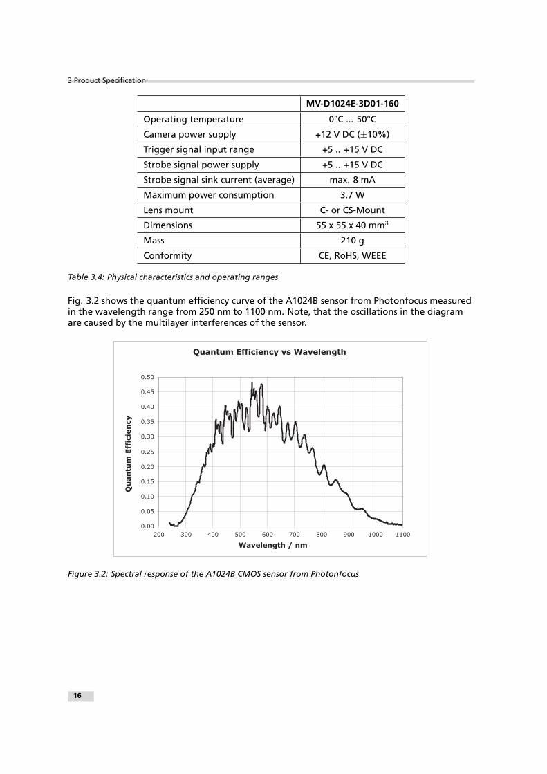
Fig. 3.2 shows the quantum efficiency curve of the A1024B sensor from Photonfocus measuredin the wavelength range from 250 nm to 1100 nm. Note, that the oscillations in the diagramare caused by the multilayer interferences of the sensor.
Q u a n t u m E f f i c i e n c y v s W a v e l e n g t h
0 . 0 0
0 . 0 5
0 . 1 0
0 . 1 5
0 . 2 0
0 . 2 5
0 . 3 0
0 . 3 5
0 . 4 0
0 . 4 5
0 . 5 0
2 0 0 3 0 0 4 0 0 5 0 0 6 0 0 7 0 0 8 0 0 9 0 0 1 0 0 0 1 1 0 0W a v e l e n g t h / n m
Quan
tum
Effi
cienc
y
Figure 3.2: Spectral response of the A1024B CMOS sensor from Photonfocus
.
16

3.4 Frame Grabber relevant Configuration
Table 3.5 summarizes the parameters needed for the configuration of the frame grabber.
MV-D1024E-3D01-160
Pixel Clock per Tap 80 MHz
Number of Taps 2
Greyscale resolution 12 bit / 10 bit / 8 bit
CC1 EXSYNC
CC2 not used
CC3 not used
CC4 not used
Table 3.5: Summary of parameters needed for frame grabber configuration
CameraLink Port and Bit assignments are compliant to the CameraLink standard (see [CL] ).
Bit Tap 0 Tap 1 Tap 0 Tap 1 Tap 0 Tap 1
8 Bit 8 Bit 10 Bit 10 Bit 12 Bit 12 Bit
0 (LSB) A0 B0 A0 C0 A0 C0
1 A1 B1 A1 C1 A1 C1
2 A2 B2 A2 C2 A2 C2
3 A3 B3 A3 C3 A3 C3
4 A4 B4 A4 C4 A4 C4
5 A5 B5 A5 C5 A5 C5
6 A6 B6 A6 C6 A6 C6
7 (MSB of 8 Bit) A7 B7 A7 C7 A7 C7
8 - - B0 B4 B0 B4
9 (MSB of 10 Bit) - - B1 B5 B1 B5
10 - - - - B2 B6
11 (MSB of 12 Bit) - - - - B3 B7
Table 3.6: CameraLink port and bit assignments for the MV-D1024E-3D01-160 camera
The output of grey values is listed in Table 3.6. 3D data are assigned in the bits [7:0]. Forfurther information see Section 4.8.3.
.
3.4 Frame Grabber relevant Configuration 17

3 Product Specification
18

4Functionality
This chapter serves as an overview of the camera configuration modes and explains camerafeatures. The goal is to describe what can be done with the camera. The setup of the camera isexplained in later chapters.
4.1 Image Acquisition
4.1.1 Readout Modes
The MV-D1024E-3D01-160 camera provides two different readout modes:
Sequential readout:
Frame time is the sum of exposure time and readout time. Exposure time of the next imagecan only start if the readout time of the current image is finished.
Simultaneous readout (interleave):
The frame time is determined by the maximum of the exposure time or of the readout time,which ever of both is the longer one. Exposure time of the next image can start during thereadout time of the current image.
MV-D1024E-3D01-160
Sequential readout available
Simultaneous readout available
Table 4.1: Readout modes of the MV-D1024E-3D01-160 camera
Fig. 4.1 illustrates the effect on the frame rate when using either the sequential readout modeor the simultaneous readout mode (interleave exposure).
Sequential readout mode:
For the calculation of the frame rate only a single formula applies: frames per second equal tothe invers of the sum of exposure time and readout time.
Simultaneous readout mode (exposure time < readout time):
The frame rate is given by the readout time. Frames per second equal to the invers of thereadout time.
Simultaneous readout mode (exposure time > readout time):
The frame rate is given by the exposure time. Frames per second equal to the invers of theexposure time.The simultaneous readout mode allows to achieve a higher frame rate. However, if theexposure time strongly exceeds the readout time, then the effect on the frame rate isneglectable.
19

4 Functionality
E x p o s u r e t i m e
F r a m e r a t e( f p s ) S i m u l t a n e o u s
r e a d o u t m o d e
S e q u e n t i a lr e a d o u t m o d e
f p s = 1 / r e a d o u t t i m e
f p s = 1 / e x p o s u r e t i m e
f p s = 1 / ( r e a d o u t t i m e + e x p o s u r e t i m e )
e x p o s u r e t i m e < r e a d o u t t i m e e x p o s u r e t i m e > r e a d o u t t i m e
e x p o s u r e t i m e = r e a d o u t t i m e
Figure 4.1: Frame rate in sequential readout mode and simultaneous readout mode
In simultaneous readout mode image output faces minor limitations. The overalllinear sensor reponse is partially restricted in the lower grey scale region.
When changing readout mode from sequential to simultaneous readout modeor vice versa, new settings of the BlackLevelOffset and of the image correctionare required.
Sequential readout:
By default the camera continuously delivers images as fast as possible ("Free-running mode")in the sequential readout mode. Exposure time of the next image can only start if the readouttime of the current image is finished.
e x p o s u r e r e a d o u t e x p o s u r e r e a d o u t
Figure 4.2: Timing in free-running sequential readout mode
When the acquisition of an image needs to be synchronised to an external event, an externaltrigger can be used (refer to Section 4.6 and Section 5.4). In this mode, the camera is idle untilit gets a signal to capture an image.
e x p o s u r e r e a d o u t i d l e e x p o s u r e
e x t e r n a l t r i g g e r
Figure 4.3: Timing in triggered sequential readout mode
20
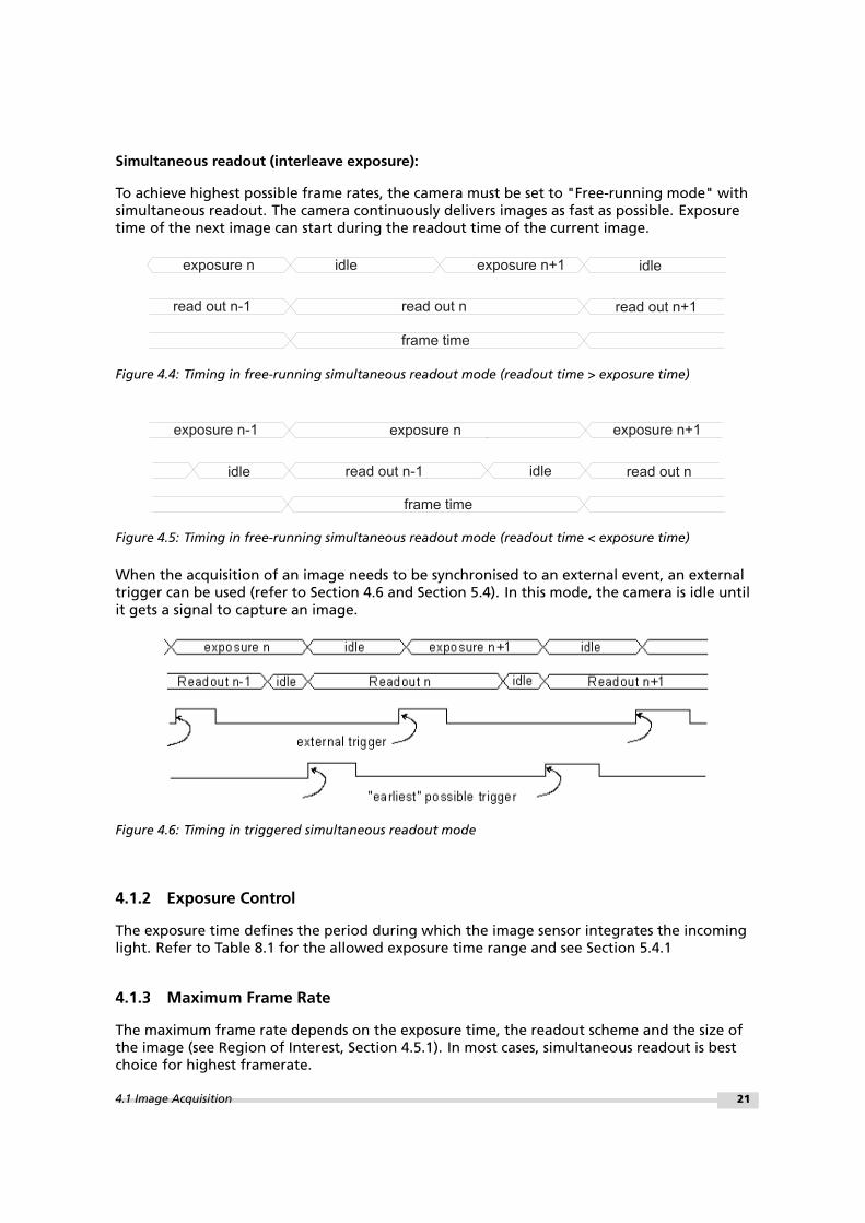
Simultaneous readout (interleave exposure):
To achieve highest possible frame rates, the camera must be set to "Free-running mode" withsimultaneous readout. The camera continuously delivers images as fast as possible. Exposuretime of the next image can start during the readout time of the current image.
e x p o s u r e n i d l e i d l e
r e a d o u t n
e x p o s u r e n + 1
r e a d o u t n + 1f r a m e t i m e
r e a d o u t n - 1
Figure 4.4: Timing in free-running simultaneous readout mode (readout time > exposure time)
e x p o s u r e n
i d l e r e a d o u t n
e x p o s u r e n + 1
f r a m e t i m er e a d o u t n - 1 i d l e
e x p o s u r e n - 1
Figure 4.5: Timing in free-running simultaneous readout mode (readout time < exposure time)
When the acquisition of an image needs to be synchronised to an external event, an externaltrigger can be used (refer to Section 4.6 and Section 5.4). In this mode, the camera is idle untilit gets a signal to capture an image.
Figure 4.6: Timing in triggered simultaneous readout mode
4.1.2 Exposure Control
The exposure time defines the period during which the image sensor integrates the incominglight. Refer to Table 8.1 for the allowed exposure time range and see Section 5.4.1
4.1.3 Maximum Frame Rate
The maximum frame rate depends on the exposure time, the readout scheme and the size ofthe image (see Region of Interest, Section 4.5.1). In most cases, simultaneous readout is bestchoice for highest framerate.
4.1 Image Acquisition 21
4 Functionality
Skimming is not supported in simultaneous readout mode.
4.1.4 Constant Frame Rate (CFR)
When the CFR mode is switched on, the frame rate (number of frames per second) can bevaried from almost 0 up to the maximum frame rate. Thus, fewer images can be acquired thanwould otherwise be possible.When Constant Frame Rate is switched off, the camera delivers images as fast as possible,depending on the exposure time and the read-out time. See Section 5.3.2 for moreinformation.
Constant Frame Rate mode (CFR) is not available together with external triggermode.
4.2 Image Information
There are camera properties available that give information about the acquired images, suchas an image counter, average image value and the number of missed trigger signals. Theseproperties can be queried by software. Alternatively, a status line within the image data can beswitched on that contains all the available image information.
4.2.1 Counters and Average Value
Image counter:
The image counter provides a sequential number of every image that is output. After camerastartup, the counter counts up from 0 (counter width 24 bit). The counter can be reset by thecamera control software.
Missed trigger counter:
The missed trigger counter counts trigger pulses that were ignored by the camera because theyoccurred within the exposure or read-out time of an image. In free-running mode it counts allincoming external triggers (counter width 8 bit / no wrap around).
Average image value:
The average image value gives the average of an image in 12 bit format (0 .. 4095 DN),regardless of the currently used grey level resolution.
.
22

4.2.2 Status Line
If enabled, the status line replaces the last row of the image with image information. Itcontains the properties described above and additional information. Every parameter is codedinto 4 pixels (LSB first) and uses the lower 8 bits of the pixel value, so that the total size of aparameter is 32 bit. The remaining pixels (24..1024) are set to 0.
4 8 1 2 1 6 2 0
P r e a m b l e0 x 5 5 A A 0 0 F F I m a g e C o u n t e r T i m e C o u n t e r
M i s s e d T r i g g e rC o u n t e r
I m a g e A v e r a g eV a l u e E x p o s u r e C y c l e s
0P i x e l :
P a r a m e t e rN a m e :
1 2 3 5 6 7 9 1 0 1 1 1 3 1 4 1 5 1 7 1 8 1 9 2 1 2 2 2 3L S B M S B
Figure 4.7: Status line parameters replace the last row of the image
The status line is also available when using an ROI. For an ROI with a width <24pixels, the status line will be clipped.
The first two data fields of the status line (preamble and image counter) are alsotransmitted on the 3D data (in either of the output modes "2D and 3D" or "3D").
Preamble:
The first parameter contains a constant value of 0x55AA00FF as a preamble in order to allowthe image processing system to easily recognise the beginning of the status line.
Image counter:
See Section 4.2.1.
Time counter:
The time counter starts at 0 after camera start, and counts real-time in units of 1 micro-second.The time counter can be reset by the software in the SDK (Counter width 32 bit).
Missed trigger counter:
See Section 4.2.1.
Average image value:
See Section 4.2.1.
Exposure cycles:
The exposure cycles parameter outputs the current exposure time in units of clock cycles (seeTable 8.1).
4.2 Image Information 23
4 Functionality
4.3 Pixel Response
4.3.1 Linear Response
The camera offers a linear response between input light signal and output grey level. This canbe modified by the use of LinLog®or Skimming as described in the following sections. Inaddition, a linear digital gain may be applied, as follows. Please see Table 3.2 for moremodel-dependent information.
Gain x1, x2, x4
Gain x1, x2 and x4 are digital amplifications, which means that the digital image data aremultiplied in the camera by a factor 1, 2 or 4, respectively.
Black Level Adjustment
The black level is the average image value at no light intensity. It can be adjusted by thesoftware by changing the black level offset. Thus, the overall image gets brighter or darker.Use a histogram to control the settings of the black level.
4.3.2 LinLog®
Overview
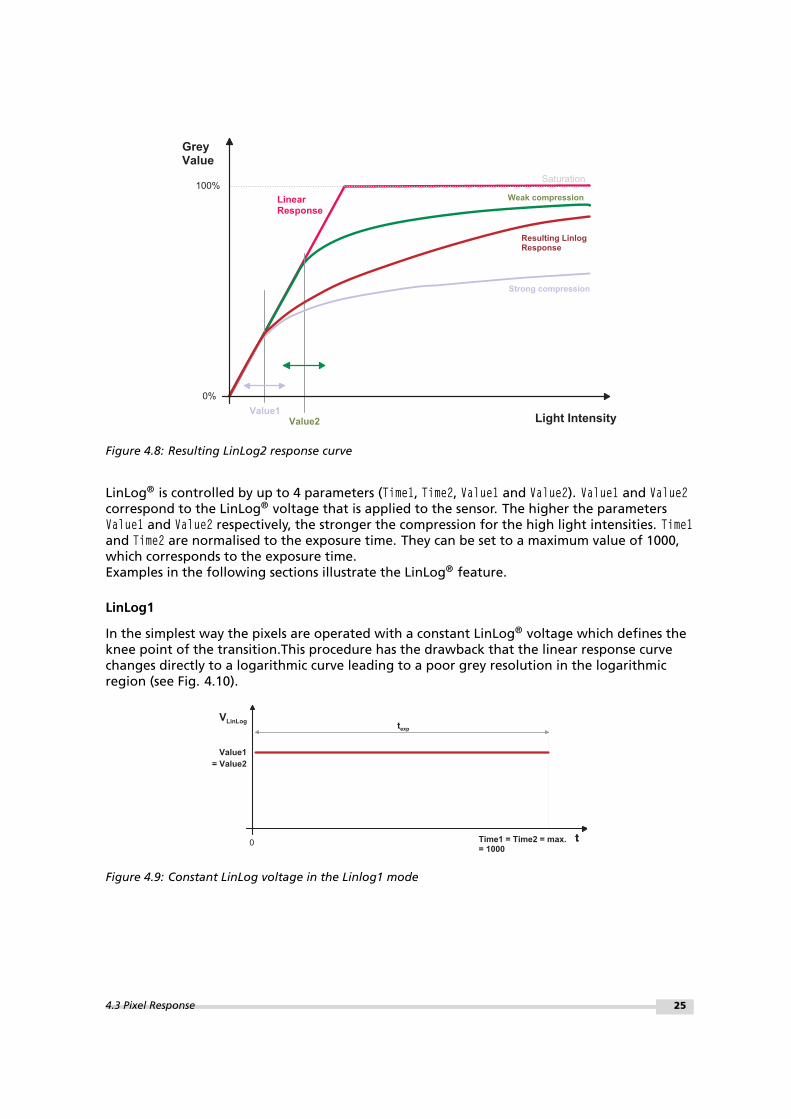
The LinLog® technology from Photonfocus allows a logarithmic compression of high lightintensities inside the pixel. In contrast to the classical non-integrating logarithmic pixel, theLinLog® pixel is an integrating pixel with global shutter and the possibility to control thetransition between linear and logarithmic mode.In situations involving high intrascene contrast, a compression of the upper grey level regioncan be achieved with the LinLog® technology. At low intensities each pixel shows a linearresponse. At high intensities the response changes to logarithmic compression (see Fig. 4.8).The transition region between linear and logarithmic response can be smoothly adjusted bysoftware and is continuously differentiable and monotonic.
.
24
G r e yV a l u e
L i g h t I n t e n s i t y0 %
1 0 0 %L i n e a r R e s p o n s e
S a t u r a t i o nW e a k c o m p r e s s i o n
V a l u e 2
S t r o n g c o m p r e s s i o n
V a l u e 1
R e s u l t i n g L i n l o gR e s p o n s e
Figure 4.8: Resulting LinLog2 response curve
LinLog® is controlled by up to 4 parameters (Time1, Time2, Value1 and Value2). Value1 and Value2correspond to the LinLog® voltage that is applied to the sensor. The higher the parametersValue1 and Value2 respectively, the stronger the compression for the high light intensities. Time1and Time2 are normalised to the exposure time. They can be set to a maximum value of 1000,which corresponds to the exposure time.Examples in the following sections illustrate the LinLog® feature.
LinLog1
In the simplest way the pixels are operated with a constant LinLog® voltage which defines theknee point of the transition.This procedure has the drawback that the linear response curvechanges directly to a logarithmic curve leading to a poor grey resolution in the logarithmicregion (see Fig. 4.10).
tt
V a l u e 1
t e x p
0
V L i n L o g
= V a l u e 2
T i m e 1 = T i m e 2 = m a x .= 1 0 0 0
Figure 4.9: Constant LinLog voltage in the Linlog1 mode
.
4.3 Pixel Response 25

4 Functionality
0
50
100
150
200
250
300
Typical LinLog1 Response Curve − Varying Parameter Value1
Illumination Intensity
Out
put g
rey
leve
l (8
bit)
[DN
]
V1 = 15
V1 = 16
V1 = 17
V1 = 18
V1 = 19
Time1=1000, Time2=1000, Value2=Value1
Figure 4.10: Response curve for different LinLog settings in LinLog1 mode
LinLog2
To get more grey resolution in the LinLog® mode, the LinLog2 procedure was developed. InLinLog2 mode a switching between two different logarithmic compressions occurs during theexposure time (see Fig. 4.11). The exposure starts with strong compression with a highLinLog®voltage (Value1). At Time1 the LinLog®voltage is switched to a lower voltage resulting ina weaker compression. This procedure gives a LinLog®response curve with more greyresolution. Fig. 4.12 and Fig. 4.13 show how the response curve is controlled by the threeparameters Value1, Value2 and the LinLog®time Time1.
Settings in LinLog2 mode, enable a fine tuning of the slope in the logarithmicregion.
tt
V a l u e 1
V a l u e 2
T i m e 1
t e x p
0
V L i n L o g
T i m e 2 = m a x .= 1 0 0 0
T i m e 1
Figure 4.11: Voltage switching in the Linlog2 mode
.
26

0
50
100
150
200
250
300
Typical LinLog2 Response Curve − Varying Parameter Time1
Illumination Intensity
Out
put g
rey
leve
l (8
bit)
[DN
]
T1 = 840
T1 = 920
T1 = 960
T1 = 980
T1 = 999
Time2=1000, Value1=19, Value2=14
Figure 4.12: Response curve for different LinLog settings in LinLog2 mode
0
20
40
60
80
100
120
140
160
180
200
Typical LinLog2 Response Curve − Varying Parameter Time1
Illumination Intensity
Out
put g
rey
leve
l (8
bit)
[DN
]
T1 = 880T1 = 900T1 = 920T1 = 940T1 = 960T1 = 980T1 = 1000
Time2=1000, Value1=19, Value2=18
Figure 4.13: Response curve for different LinLog settings in LinLog2 mode
4.3 Pixel Response 27
4 Functionality
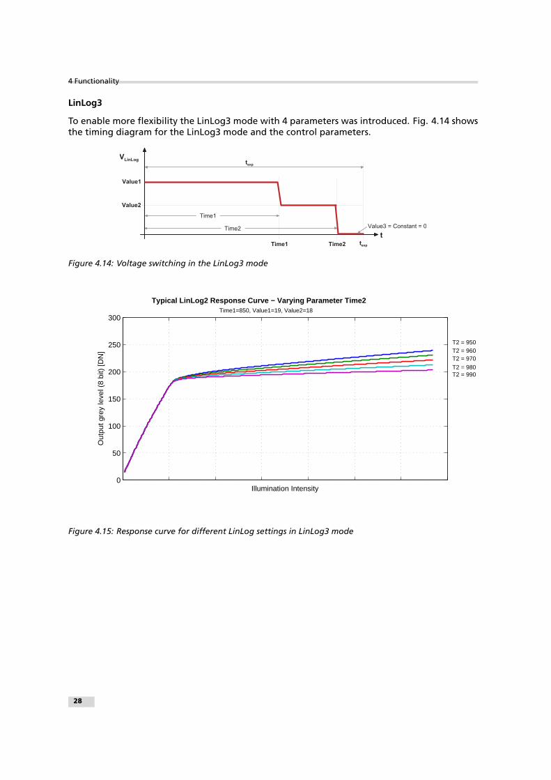
LinLog3
To enable more flexibility the LinLog3 mode with 4 parameters was introduced. Fig. 4.14 showsthe timing diagram for the LinLog3 mode and the control parameters.
V L i n L o g
t
V a l u e 1
V a l u e 2
t e x p
T i m e 2T i m e 1
T i m e 1 T i m e 2 t e x p
V a l u e 3 = C o n s t a n t = 0
Figure 4.14: Voltage switching in the LinLog3 mode
0
50
100
150
200
250
300
Typical LinLog2 Response Curve − Varying Parameter Time2
Illumination Intensity
Out
put g
rey
leve
l (8
bit)
[DN
]
T2 = 950 T2 = 960 T2 = 970
T2 = 980 T2 = 990
Time1=850, Value1=19, Value2=18
Figure 4.15: Response curve for different LinLog settings in LinLog3 mode
28
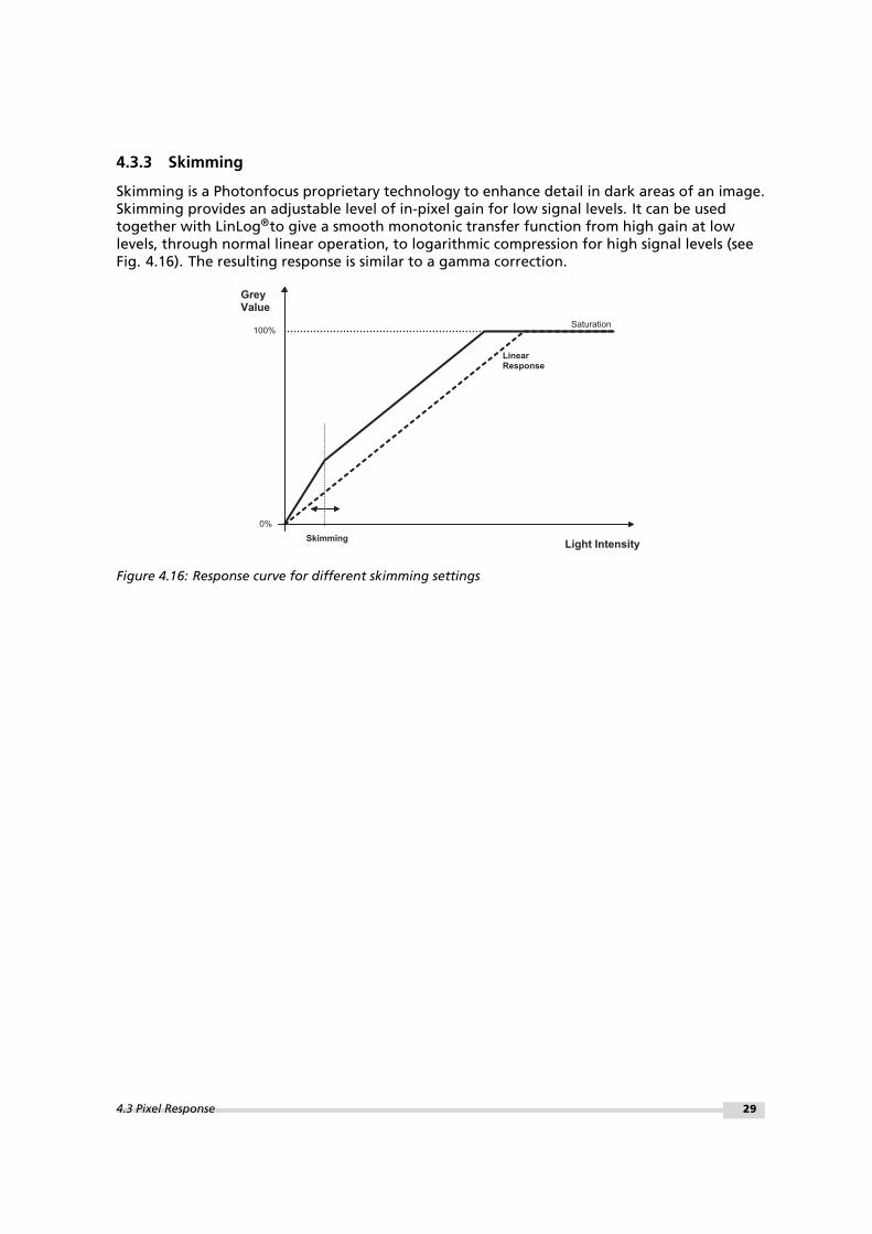
4.3.3 Skimming
Skimming is a Photonfocus proprietary technology to enhance detail in dark areas of an image.Skimming provides an adjustable level of in-pixel gain for low signal levels. It can be usedtogether with LinLog®to give a smooth monotonic transfer function from high gain at lowlevels, through normal linear operation, to logarithmic compression for high signal levels (seeFig. 4.16). The resulting response is similar to a gamma correction.
G r e yV a l u e
L i g h t I n t e n s i t y0 %
1 0 0 %
L i n e a r R e s p o n s e
S a t u r a t i o n
S k i m m i n g
Figure 4.16: Response curve for different skimming settings
4.3 Pixel Response 29

4 Functionality
4.3.4 Grey Level Transformation (LUT)
Grey level transformation is remapping of the grey level values of an input image to newvalues. The look-up table (LUT) is used to convert the greyscale value of each pixel in an imageinto another grey value. It is typically used to implement a transfer curve for contrastexpansion. The camera performs a 10-to-8-bit mapping, so that 1024 input grey levels can bemapped to 256 output grey levels. The use of the three available modes is explained in thenext sections.
The output grey level resolution of the look-up table (independent of gain,gamma or user-definded mode) is always 8 bit.
There are 2 predefined functions, which generate a look-up table and transfer itto the camera. For other transfer functions the user can define his own LUT file.
Gain
The ’Gain’ mode performs a digital, linear amplification (see Fig. 4.17). It is configurable in therange from 1.0 to 4.0 (e.g. 1.234).
0 200 400 600 800 1000 12000
50
100
150
200
250
300Grey level transformation − Gain: y = (255/1023) ⋅ a ⋅ x
x: grey level input value (10 bit) [DN]
y: g
rey
leve
l out
put v
alue
(8
bit)
[DN
]
a = 1.0a = 2.0a = 3.0a = 4.0
Figure 4.17: Applying a linear gain to an image
30

Gamma
The ’Gamma’ mode performs an exponential amplification, configurable in the range from 0.4to 4.0. Gamma > 1.0 results in an attenuation of the image (see Fig. 4.18), gamma < 1.0 resultsin an amplification (see Fig. 4.19).
0 200 400 600 800 1000 12000
50
100
150
200
250
300Grey level transformation − Gamma: y = (255 / 1023γ) ⋅ xγ (γ ≥ 1)
x: grey level input value (10 bit) [DN]
y: g
rey
leve
l out
put v
alue
(8
bit)
[DN
]
γ = 1.0γ = 1.2γ = 1.5γ = 1.8γ = 2.5γ = 4.0
Figure 4.18: Applying gamma correction to an image (gamma > 1)
0 200 400 600 800 1000 12000
50
100
150
200
250
300Grey level transformation − Gamma: y = (255 / 1023γ) ⋅ xγ (γ ≤ 1)
x: grey level input value (10 bit) [DN]
y: g
rey
leve
l out
put v
alue
(8
bit)
[DN
]
γ = 1.0γ = 0.9γ = 0.8γ = 0.6γ = 0.4
Figure 4.19: Applying gamma correction to an image (gamma < 1)
4.3 Pixel Response 31

4 Functionality
User-defined Look-up Table
In the ’User’ mode, the mapping of input to output grey levels can be configured arbitrarily bythe user. There is an example file in the PFRemote folder.
U s e r L U Ty = f ( x )
1 0 b i t 8 b i t
Figure 4.20: Data path through LUT
4.3.5 Test Images
Test images are generated in the camera FPGA, independent of the image sensor. They can beused to check the transmission path from the camera to the frame grabber. Independent fromthe configured grey level resolution, every possible grey level appears the same number oftimes in a test image. Therefore, the histogram of the received image must be flat.
A test image is a useful tool to find data transmission errors that are caused mostoften by a defective cable between camera and frame grabber.
Test images give the correct result at full resolution only.
Ramp
Depending on the configured grey level resolution, the ramp test image outputs a constantpattern with increasing grey level from the left to the right side (see Fig. 4.21).
Figure 4.21: Ramp test images: 8 bit output (left), 10 bit output (middle), 12 bit output (right)
LFSR
The LFSR (linear feedback shift register) test image outputs a constant pattern with apseudo-random grey level sequence containing every possible grey level that is repeated forevery row. In 12 bit mode only a fourth of all possible grey values appear.
32
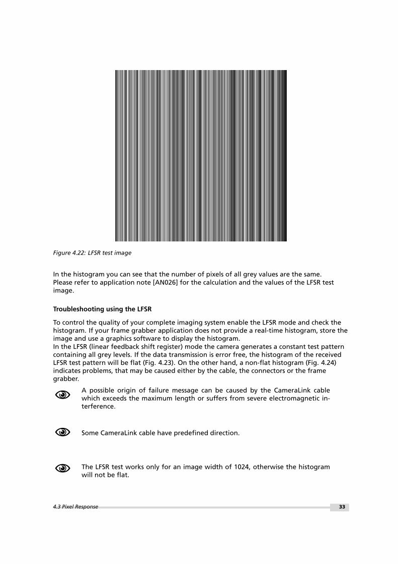
Figure 4.22: LFSR test image
In the histogram you can see that the number of pixels of all grey values are the same.Please refer to application note [AN026] for the calculation and the values of the LFSR testimage.
Troubleshooting using the LFSR
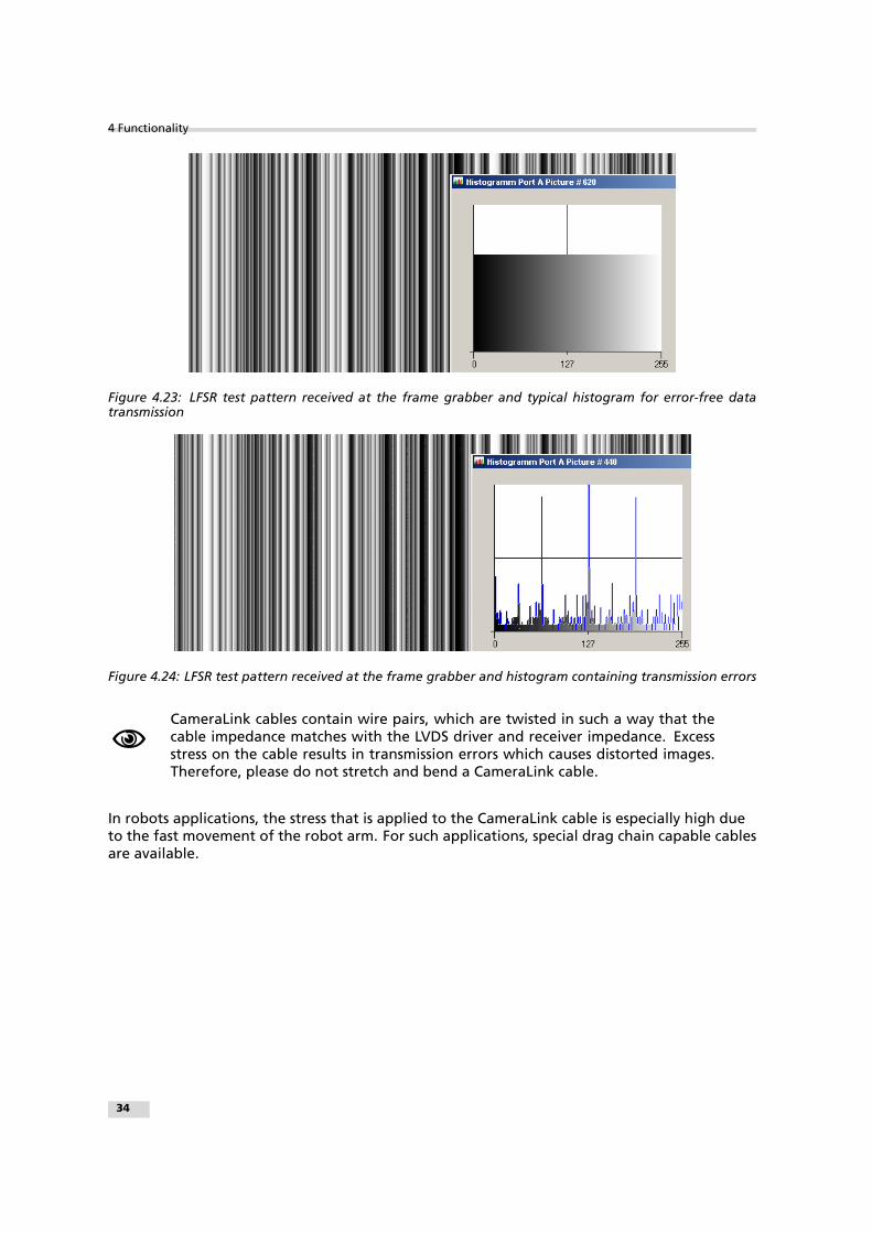
To control the quality of your complete imaging system enable the LFSR mode and check thehistogram. If your frame grabber application does not provide a real-time histogram, store theimage and use a graphics software to display the histogram.In the LFSR (linear feedback shift register) mode the camera generates a constant test patterncontaining all grey levels. If the data transmission is error free, the histogram of the receivedLFSR test pattern will be flat (Fig. 4.23). On the other hand, a non-flat histogram (Fig. 4.24)indicates problems, that may be caused either by the cable, the connectors or the framegrabber.
A possible origin of failure message can be caused by the CameraLink cablewhich exceeds the maximum length or suffers from severe electromagnetic in-terference.
Some CameraLink cable have predefined direction.
The LFSR test works only for an image width of 1024, otherwise the histogramwill not be flat.
4.3 Pixel Response 33
4 Functionality
Figure 4.23: LFSR test pattern received at the frame grabber and typical histogram for error-free datatransmission
Figure 4.24: LFSR test pattern received at the frame grabber and histogram containing transmission errors
CameraLink cables contain wire pairs, which are twisted in such a way that thecable impedance matches with the LVDS driver and receiver impedance. Excessstress on the cable results in transmission errors which causes distorted images.Therefore, please do not stretch and bend a CameraLink cable.
In robots applications, the stress that is applied to the CameraLink cable is especially high dueto the fast movement of the robot arm. For such applications, special drag chain capable cablesare available.
34
4.4 Image Correction
4.4.1 Overview
The MV-D1024E-3D01-160 camera possesses image pre-processing features, that compensatefor non-uniformities caused by the sensor, the lens or the illumination. This method ofimproving the image quality is generally known as ’Shading Correction’ or ’Flat FieldCorrection’ and consists of a combination of offset correction, gain correction and pixelinterpolation.
Since the correction is performed in hardware, there is no performance limita-tion for high frame rates.
The offset correction subtracts a configurable positive or negative value from the live imageand thus reduces the fixed pattern noise of the CMOS sensor. In addition, hot pixels can beremoved by interpolation. The gain correction can be used to flatten uneven illumination or tocompensate shading effects of a lens. Both offset and gain correction work on a pixel-per-pixelbasis, i.e. every pixel is corrected separately. For the correction, a black reference and a greyreference image are required. Then, the correction values are determined automatically in thecamera.
Do not set any reference images when gain or LUT is enabled!
Correction values of both reference images can be saved into the internal flash memory, butthis overwrites the factory presets. Then the reference images that are delivered by factorycannot be restored anymore.
4.4.2 Offset Correction (FPN, Hot Pixels)
The offset correction is based on a black reference image, which is taken at no illumination(e.g. lens aperture completely closed). The black reference image contains the fixed-patternnoise of the sensor, which can be subtracted from the live images in order to minimise thestatic noise.
Offset correction algorithm
After configuring the camera with a black reference image, the camera is ready to apply theoffset correction:
1. Determine the average value of the black reference image.
2. Subtract the black reference image from the average value.
3. Mark pixels that have a grey level higher than 1008 DN (@ 12 bit) as hot pixels.
4. Store the result in the camera as the offset correction matrix.
5. During image acquisition, subtract the correction matrix from the acquired image andinterpolate the hot pixels (see Section 4.4.2).
4.4 Image Correction 35

4 Functionality
44
4
31213 1
4 323
41
1
2 4 14
43
1
3
4
b l a c k r e f e r e n c e i m a g e
11
1
2- 12- 2- 1 0
1 - 11
- 10
2
0
- 10
- 2
0
1 1 - 2 - 2 - 2
a v e r a g eo f b l a c kr e f e r e n c ep i c t u r e
=-o f f s e t c o r r e c t i o nm a t r i x
Figure 4.25: Offset correction
How to Obtain a Black Reference Image
In order to improve the image quality, the black reference image must meet certain demands.
• The black reference image must be obtained at no illumination, e.g. with lens apertureclosed or closed lens opening.
• It may be necessary to adjust the black level offset of the camera. In the histogram of theblack reference image, ideally there are no grey levels at value 0 DN after adjustment ofthe black level offset. All pixels that are saturated black (0 DN) will not be properlycorrected (see Fig. 4.26). The peak in the histogram should be well below the hot pixelthreshold of 1008 DN @ 12 bit.
• Camera settings such as exposure time, LinLog®, skimming and digital gain may influencethe grey level. Therefore, for best results the camera settings of the black reference imagemust be identical with the camera settings of the corrected image.
0 200 400 600 800 1000 1200 1400 16000
0.2
0.4
0.6
0.8
1Histogram of the uncorrected black reference image
Grey level, 12 Bit [DN]
Rel
ativ
e nu
mbe
r of
pix
els
[−]
black level offset okblack level offset too low
Figure 4.26: Histogram of a proper black reference image for offset correction
Hot pixel correction
Every pixel that exceeds a certain threshold in the black reference image is marked as a hotpixel. If the hot pixel correction is switched on, the camera replaces the value of a hot pixel byan average of its neighbour pixels (see Fig. 4.27).
36

h o t p i x e lp np n - 1 p n + 1
p n = p n - 1 + p n + 1 2
Figure 4.27: Hot pixel interpolation
4.4.3 Gain Correction
The gain correction is based on a grey reference image, which is taken at uniform illuminationto give an image with a mid grey level.
Gain correction is not a trivial feature. The quality of the grey reference imageis crucial for proper gain correction.
Gain correction algorithm
After configuring the camera with a black and grey reference image, the camera is ready toapply the gain correction:
1. Determine the average value of the grey reference image.
2. Subtract the offset correction matrix from the grey reference image.
3. Divide the average value by the offset corrected grey reference image.
4. Pixels that have a grey level bigger than a certain threshold are marked as hot pixels.
5. Store the result in the camera as the gain correction matrix.
6. During image acquisition, multiply the gain correction matrix from the offset-correctedacquired image and interpolate the hot pixels (see Section 4.4.2).
: 71 0
9
79787 9
4 323
41
1
9 6 84
61 0
1
3
4
g r e y r e f e r e n c ep i c t u r e
a v e r a g eo f g r e y
r e f e r e n c ep i c t u r e ) 1
1 . 21
0 . 9 11 . 2- 20 . 9 1
1 - 11
0 . 81
1
0
1 . 30 . 8
1
0
1 1 - 2 - 2 - 2
=1
11
2- 12- 2- 1 0
1 - 11
- 10
2
0
- 10
- 2
0
1 1 - 2 - 2 - 2
- )o f f s e t c o r r e c t i o nm a t r i x
g a i n c o r r e c t i o nm a t r i x
Figure 4.28: Gain Correction
Gain correction always needs an offset correction matrix, so the offset correctionhas to be performed before the gain correction.
4.4 Image Correction 37

4 Functionality
How to Obtain a Grey Reference Image
In order to improve the image quality, the grey reference image must meet certain demands.
• The grey reference image must be obtained at uniform illumination.
Use a high quality light source that delivers uniform illumination. Standard illu-mination will not be appropriate.
• When looking at the histogram of the grey reference image, ideally there are no greylevels at full scale (4095 DN @ 12 bit). All pixels that are saturated white will not beproperly corrected (see Fig. 4.29).
• Camera settings such as exposure time, LinLog, skimming and digital gain may influencethe grey level. Therefore, the camera settings of the grey reference image must beidentical with the camera settings of the corrected image.
2400 2600 2800 3000 3200 3400 3600 3800 4000 42000
0.2
0.4
0.6
0.8
1Histogram of the uncorrected grey reference image
Grey level, 12 Bit [DN]
Rel
ativ
e nu
mbe
r of
pix
els
[−]
grey reference image okgrey reference image too bright
Figure 4.29: Proper grey reference image for gain correction
4.4.4 Corrected Image
Offset, gain and hot pixel correction can be switched on seperately. The followingconfigurations are possible:
• No correction
• Offset correction only
• Offset and hot pixel correction
• Hot pixel correction only
• Offset and gain correction
• Offset, gain and hot pixel correction
In addition, the black reference image and grey reference image that are currently stored inthe camera RAM can be output.Table 4.2 shows the maximum values of the correction matrices, i.e. the error range that theoffset and gain algorithm can correct.
.
38

57
6
57665 6
4 373
47
1
7 4 64
43
1
3
4
c u r r e n t i m a g e
) 56
6
55655 4
4 373
47
1
7 4 64
43
1
3
4)1
11
2- 12- 2- 1 0
1 - 11
- 10
2
0
- 10
- 2
0
1 1 - 2 - 2 - 2
o f f s e t c o r r e c t i o nm a t r i x
- 11 . 2
1
0 . 9 11 . 2- 20 . 9 1
1 - 11
0 . 81
1
0
1 . 30 . 8
1
0
1 1 - 2 - 2 - 2
g a i n c o r r e c t i o nm a t r i x
=.c o r r e c t e d i m a g e
)Figure 4.30: Corrected image
minimum maximum
Offset correction -508 DN @ 12 bit +508 DN @ 12 bit
Gain correction 0.42 2.67
Table 4.2: Offset and gain correction ranges
4.5 Reduction of Image Size
With Photonfocus cameras there are several possibilities to focus on the interesting parts of animage, thus reducing the data rate and increasing the frame rate. The most commonly usedfeature is Region of Interest (ROI).
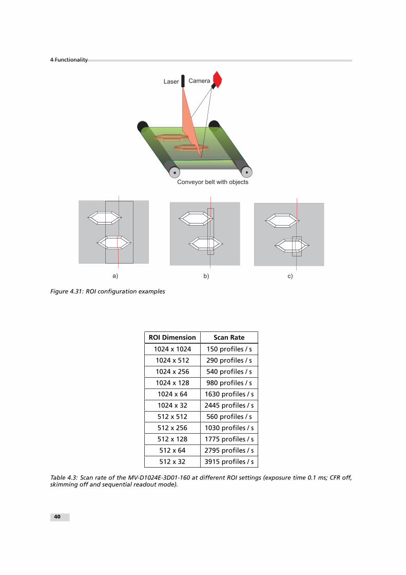
4.5.1 Region of Interest (ROI)
Some applications do not need full image resolution (e.g. 1024 x 1024 pixels). By reducing theimage size to a certain region of interest (ROI), the frame rate can be drastically increased. Aregion of interest can be almost any rectangular window and is specified by its position withinthe full frame and its width and height. Fig. 4.32 gives some possible configurations for aregion of interest, and Table 4.3 shows some numerical examples of how the frame rate can beincreased by reducing the ROI.
To optimize the scan rate of the MV-D1024E-3D01-160 reduce the region of in-terest to the smallest possible setting (see Table 4.3).
Both reductions in x- and y-direction result in a higher frame rate.
.
4.5 Reduction of Image Size 39
4 Functionality
C o n v e y o r b e l t w i t h o b j e c t s
L a s e r C a m e r a
a ) b ) c )
Figure 4.31: ROI configuration examples
ROI Dimension Scan Rate
1024 x 1024 150 profiles / s
1024 x 512 290 profiles / s
1024 x 256 540 profiles / s
1024 x 128 980 profiles / s
1024 x 64 1630 profiles / s
1024 x 32 2445 profiles / s
512 x 512 560 profiles / s
512 x 256 1030 profiles / s
512 x 128 1775 profiles / s
512 x 64 2795 profiles / s
512 x 32 3915 profiles / s
Table 4.3: Scan rate of the MV-D1024E-3D01-160 at different ROI settings (exposure time 0.1 ms; CFR off,skimming off and sequential readout mode).
40

Exposure time Sequential Readout Simultaneous Readout
10 µs 1177 profiles / s 761 profiles / s
100 µs 1064 profiles / s 761 profiles / s
500 µs 746 profiles / s 761 profiles / s
1 ms 544 profiles / s 761 profiles / s
2 ms 352 profiles / s 482 profiles / s
5 ms 171 profiles / s 197 profiles / s
10 ms 92 profiles / s 99 profiles / s
12 ms 78 profiles / s 83 profiles / s
Table 4.4: Scan rate of the MV-D1024E-3D01-160 at different exposure times, in sequential readout modeand in simultaneous readout mode at 1024 x 128 pixel resolution (CFR off and skimming off).
Calculation of the maximum frame rate
The frame rate mainly depends of the exposure time and readout time. The frame rate is theinverse of the frame time. In the following formula the minimum frame time is calculated.When using CFR mode the frame time can get extended.
fps = 1tframe
Calculation of the frame time (sequential mode)
tframe ≥ texp + tro + tproc + tRAM
Calculation of the frame time (simultaneous mode)
tframe ≥ max(texp + 76 µs, tro + 476 µs) + tRAM
tro = tCLK * (Py * ( Pxtaps + LP) + LP)
tproc = tNormal + tCFR + tFPN + tSkim
tRAM = 1128 * (tro + 1375 ns) - (texp + tproc)
When the result of tRAM is negative, set it to 0.
4.5 Reduction of Image Size 41
4 Functionality
tframe frame time
texp exposure time
tro readout time
tproc processing time
tRAM RAM refresh time
tNormal constant latency
tCFR constant frame rate latency, only when CFR is enabled
tFPN correction latency, only when correction is enabled
tSkim skim latency, only when Skimming is enabled
tCLK pixel clock
taps CameraLink taps
PX number of pixels in x-direction
PY number of pixels in y-direction (+1, for the MV-D1024E-3D01-160)
LP line pause, constant LP = 8 for all models
MV-D1024E-3D01-160
texp 10 µs - 419 ms
tNormal 1300 ns
tCFR 0
tFPN 0
tSkim 50.8 µs
tCLK 12.5 ns
taps 2
PY Window H + 1
Table 4.5: Camera specific values for frame time calculations
A calculator for calculating the maximum frame rate is available in the supportarea of the Photonfocus website.
4.5.2 Multiple Regions of Interest
The MV-D1024E-3D01-160 camera can handle up to 16 different regions of interest. Thisfeature can be used to reduce the image data and increase the frame rate. The multiple ROIsare joined together and form a single image, which is transferred to the frame grabber.An ROI is defined by its starting value in y-direction and its height. Every ROI within a MROImust be of the same width. The maximum frame rate in MROI mode depends on the numberof rows and columns being read out. Overlapping ROIs are allowed. See Section 4.5.1 forinformation on the calculation of the maximum frame rate.
42

C o n v e y o r b e l t w i t h o b j e c t s
L a s e r C a m e r a
a ) b )
Figure 4.32: Multiple Regions of Interest with 2 ROIs
4.5.3 Decimation
Decimation reduces the number of pixels in y-direction. Decimation can also be used togetherwith ROI or MROI. Decimation in y-direction transfers every nthrow only and directly results inreduced read-out time and higher frame rate respectively.
4.6 External Trigger
An external trigger is an event that starts an exposure. The trigger signal is either generatedon the frame grabber (soft-trigger) or comes from an external device such as a light barrier. If atrigger signal is applied to the camera before the earliest time for the next trigger, this triggerwill be ignored. The camera property Counter.MissedTrigger stores the number of triggerevents which where ignored.
4.6.1 Trigger Source
The trigger signal can be configured to be active high or active low. One of the followingtrigger sources can be used:
Interface Trigger In the interface trigger mode, the trigger signal is applied to the camera bythe CameraLink interface.
I/O Trigger In the I/O trigger mode, the trigger signal is applied directly to the camera by thepower supply connector (over an optocoupler).
4.6 External Trigger 43

4 Functionality
I n t e r f a c e T r i g g e rD A T A
C a m e r a
o p t oI / O
C LF r a m e g r a b b e r
A n y T r i g g e rS o u r c eI / O T r i g g e r
A n y T r i g g e rS o u r c e
Figure 4.33: Trigger Inputs
4.6.2 Trigger Mode
Depending on the trigger mode, the exposure time can be determined either by the camera orby the trigger signal itself:
Camera-controlled Exposure In this trigger mode the exposure time is defined by the camera.For an active high trigger signal, the camera starts the exposure with a positive triggeredge and stops it when the preprogrammed exposure time has elapsed. The exposuretime is defined by the software.
Level-controlled Exposure In this trigger mode the exposure time is defined by the pulse widthof the trigger pulse. For an active high trigger signal, the camera starts the exposure withthe positive edge of the trigger signal and stops it with the negative edge.
Level-controlled Exposure is not available in simultaneous readout mode.
Figure 4.35 gives an overview over the available trigger modes. The signal ExSync stands for thetrigger signal, which is provided either through the interface or the I/O trigger. For moreinformation and the respective timing diagrams see Section 5.4
C a m e r a c o n t r o l l e d e x p o s u r eL e v e l c o n t r o l l e d e x p o s u r e
E x p o s u r e S t a r t E x p o s u r e S t o p
E x S y n c C a m e r a
E x S y n c E x S y n c
P o l a r i t y A c t i v e H i g hE x p o s u r e S t a r t E x p o s u r e S t o p
E x S y n c C a m e r a
E x S y n c E x S y n c
P o l a r i t y A c t i v e L o w
R i s i n g E d g eF a l l i n g E d g e
Figure 4.34: Trigger Inputs
4.6.3 Trigger Delay
Programmable delay in milliseconds between the incoming trigger edge and the start of theexposure. This feature may be required to synchronize to external strobe with the exposure ofthe camera.
44

4.6.4 Trigger Resolution
For a succesfull 3D image acquisition it is important to use the encoder pulses from theconveyer belt or a similar device for triggering the image acquisition of the camera. However,it may occur that the delivered encoder pulse frequency exceeds the requirements of the 3Dapplication. To allow for exact configuration of the image acquisition system the TriggerResolution feature allows to skip a predefined number of trigger pulses delivered from theincremental encoder.
E N C O D E RT R I G G E R P U L S EU S E DT R I G G E RP U L S E
Figure 4.35: Timing in Trigger Resolution mode. Example: Applying a Trigger Resolution value of 2 willskip two trigger pulses from the incremental encoder and capture images upon every 3rd trigger pulse.
4.7 Strobe Output
The strobe output is an opto-isolated output located on the power supply connector that canbe used to trigger a strobe. The strobe output can be used both in free-running and in triggermode. There is a programmable delay available to adjust the strobe pulse to your application.
The strobe output needs a separate power supply. Please see Section 5.1.3 formore information.
.
4.7 Strobe Output 45

4 Functionality
4.8 Additional 3D Functionality
4.8.1 Mode Settings
The Peak Detector functionality in the MV-D1024E-3D01-160 camera can be configured indifferent modes, depending on what image information should be transfered from the camerato the frame grabber. The following settings can be selected:
2D Mode
In the 2D mode the camera sends raw image data to the frame grabber, which can then befurther processed on the frame grabber or by an image processing software tool. Noadditional 3D information is transferred with the raw image data when using the 2D mode.
Combined 2D/3D Mode
In the combined 2D/3D mode the camera sends the raw image data including the necessary 3Dinformation to the frame grabber. The raw image containing the laser line is analyzed by thePeak Detector in the camera’s FPGA. This 3D information is then attached to the 2D raw image.
The laser line needs to be aligned in vertical orientation towards the camera.
Only a single vertical laser line can be processed at a time by the 3D Peak Detec-tor algorithm.
. If your application requires to process multiple laser lines please contact Photon-focus to discuss possible firmware adaptions.
The combined 2D/3D mode is typically used for simultaneous image analysis of 2D and 3Dimages or to set up the laser triangulation system.
3D Mode
In the 3D mode the camera only sends the 3D data calculated by the Peak Detector algorithmin the camera FPGA to the frame grabber.
4.8.2 Threshold
The raw image data are first processed by the threshold pre-filter before being analyzed by thePeak Detector algorithm.
The threshold must be set above the image background otherwise the 3D datamay be incorrect.
.
46
0 . 2 Q u a l i t y W i d t h
Inten
sity
x - d i r e c t i o n
Q u a l i t y
G a u s s i a n s h a p e d l a s e r l i n e
Figure 4.36: The peak width is determined by the subtraction of a baseline, that equals 0.2 quality
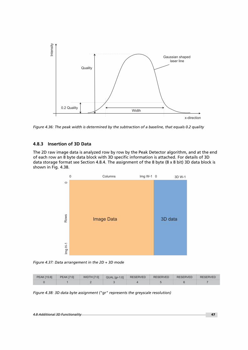
4.8.3 Insertion of 3D Data
The 2D raw image data is analyzed row by row by the Peak Detector algorithm, and at the endof each row an 8 byte data block with 3D specific information is attached. For details of 3Ddata storage format see Section 4.8.4. The assignment of the 8 byte (8 x 8 bit) 3D data block isshown in Fig. 4.38.
I m a g e D a t a 3 D d a t aRows
C o l u m n s 3 D W - 1I m g W - 10 0
Img H
-10
Figure 4.37: Data arrangement in the 2D + 3D mode
P E A K [ 1 5 : 8 ]0
P E A K [ 7 : 0 ]1
W I D T H [ 7 : 0 ]2
Q U A L [ g r - 1 : 0 ]3
R E S E R V E D4
R E S E R V E D5
R E S E R V E D6
R E S E R V E D7
Figure 4.38: 3D data byte assignment ("gr" represents the greyscale resolution)
.
4.8 Additional 3D Functionality 47

4 Functionality
The 3D data block contains the following information:
• Peak coordinate (2 bytes). The 1st and the 2nd byte (PEAK [15:0]) indicate the calculatedpeak position of the laser line within the 2D raw image. PEAK [15:6] is the integer part ofthe peak coordinate and PEAK [5:0] is the fractional part.
• Laser line width (1 byte). The 3rd byte (WIDTH [7:0]) contains the width of the laser line(see Fig. 4.36). WIDTH [7:2] is the integer part and WIDTH [1:0] is the fractional part.
• Detection quality indicator (1 word). The 4th byte (QUAL [(gr-1):0]) contains the maximumheight of the laser line (see Fig. 4.36). For the bit assignment of the quality indicator in 8bit, 10 bit or 12 bit greyscale resolution see Table 4.6. In this context the abbreviation "gr"is used for the greyscale resolution (8 bit, 10 bit or 12 bit).
• Reserved (4 byte).
Greyscale Resolution Quality Indicator
8 bit QUAL[7:0]
10 bit QUAL[9:0]
12 bit QUAL[11:0]
Table 4.6: Bit assignment of the quality indicator depends on the greyscale resolution
The 3D data block is always given in 8 bit format, independent of the choosengreyscale resolution, except QUAL. The 8 bit data is located on the LSBs of thepixel and the remaining bits are set to 0.
4.8.4 Interpolation Technique
Structured light based systems crucially rely on an accurate determination of the peak positionof the Gaussian shaped laser line. The Peak Detector algorithm in the MV-D1024E-3D01-160camera applies nonlinear interpolation techniques, where up to 64 data points can be insertedbetween two pixels within the Gaussian shaped laser line. This technique is superior to othercommonly used detection techniques, such as the detection of peak pixel intensity across thelaser line (resulting in pixel accuracy) or the thresholding of the Gaussian and calculation of theaverage (resulting in subpixel accuracy).
The Peak Detector analyzes all image data that are enclosed within the selectedregion of interest (ROI).
.
48

The nonlinear interpolation technique used in the Peak Detector algorithm results in a betterestimate of the maximum intensity of the laser line. The data mapping for the 3D data block isshown in Fig. 4.37 and the basics of the interpolation principle are illustrated in Fig. 4.39.
P E A K [ 1 5 : 6 ] P E A K [ 5 : 0 ] W I D T H [ 7 : 0 ] Q U A L [ g r - 1 : 0 ] R E S E R V E D R E S E R V E D R E S E R V E D R E S E R V E D
I n t e r p o l a t e d r e s o l u t i o n
M a x i m u m v a l u e i n t e r p o l a t i o n
G a u s s i a n s h a p e d l a s e r l i n e
0 . 2 Q u a l i t y
Width
Quali
ty
Pixel
Sub-p
ixel
Quali
ty
W i d t h
Figure 4.39: Interpolation technique provides sub-pixel accuracy in the detection of the laser peak byinserting up to 64 data points between two pixels ("gr" represents the greyscale resolution).
4.8 Additional 3D Functionality 49

4 Functionality
The line position is split into a coarse position and a fine position (sub-pixel). The coarseposition is based on the pixel pitch and is transferred in Peak [15:6]. The sub-pixel position thatwas calculated from the Peak Detector algorithm (6 bit sub-pixel information) is mapped toPeak [5:0]. The value ranges of the 3D data block are listed in Table 4.7.
If the camera is operating in a greyscale resolution mode higher than 8 bit, thenthe MSBs are filled by 0 (except for the quality indicator). This means that onlybits [7:0] contain the 3D information.
3D Data Value range
PEAK [15:6] 0 .. 1023
PEAK [5:0] 0 .. 63
WIDTH [7:0] 0 .. 63
WIDTH [1:0] 0 .. 3
QUAL [(gr-1):0] 0 .. (2gr - 1)
Table 4.7: Value ranges of the 3D data block ("gr" indicates the greyscale resolution)
4.9 Configuration Interface (CameraLink)
A CameraLink camera can be controlled by the user via a RS232 compatible asynchronous serialinterface. This interface is contained within the CameraLink interface as shown in Fig. 4.40 andis physically not directly accessible. Instead, the serial communication is usually routed throughthe frame grabber. For some frame grabbers it might be necessary to connect a serial cablefrom the frame grabber to the serial interface of the PC. .
Came
raLink
C a m e r a
I m a g e d a t a ,F V A L , L V A L , D V A L
P i x e l C l o c k
C C S i g n a l s
S e r i a l I n t e r f a c e
F r a m e -g r a b b e r
Came
raLink
Figure 4.40: CameraLink serial interface for camera communication
50

5Hardware Interface
5.1 Connectors
5.1.1 CameraLink Connector for CameraLink Camera Models
The CameraLink cameras are interfaced to external components via
• a CameraLink connector, which is defined by the CameraLink standard as a 26 pin, 0.05"Mini Delta-Ribbon (MDR) connector to transmit configuration, image data and trigger.
• a subminiature connector for the power supply, 7-pin Binder series 712.
The connectors are located on the back of the camera. Fig. 5.1 shows the plugs and the statusLED which indicates camera operation.
Figure 5.1: Rear view of the CameraLink camera
The CameraLink interface and connector are specified in [CL]. For further details including thepinout please refer to Appendix A. This connector is used to transmit configuration, imagedata and trigger signals.
5.1.2 Power Supply for CameraLink Camera Models
The camera requires a single voltage input (see Table 3.4). The camera meets all performancespecifications using standard switching power supplies, although well-regulated linear powersupplies provide optimum performance.
It is extremely important that you apply the appropriate voltages to your camera.Incorrect voltages will damage the camera.
A suitable power supply is available from Photonfocus.
For further details including the pinout please refer to Appendix A.
51
5 Hardware Interface
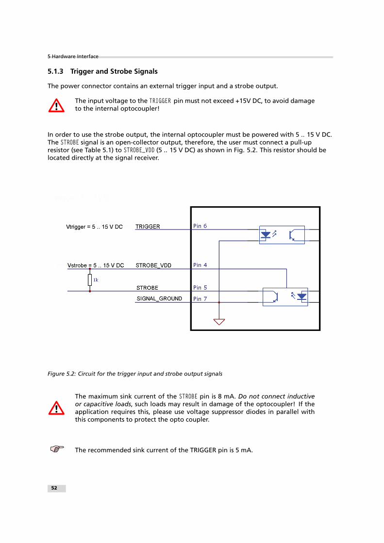
5.1.3 Trigger and Strobe Signals
The power connector contains an external trigger input and a strobe output.
The input voltage to the TRIGGER pin must not exceed +15V DC, to avoid damageto the internal optocoupler!
In order to use the strobe output, the internal optocoupler must be powered with 5 .. 15 V DC.The STROBE signal is an open-collector output, therefore, the user must connect a pull-upresistor (see Table 5.1) to STROBE_VDD (5 .. 15 V DC) as shown in Fig. 5.2. This resistor should belocated directly at the signal receiver.
Figure 5.2: Circuit for the trigger input and strobe output signals
The maximum sink current of the STROBE pin is 8 mA. Do not connect inductiveor capacitive loads, such loads may result in damage of the optocoupler! If theapplication requires this, please use voltage suppressor diodes in parallel withthis components to protect the opto coupler.
The recommended sink current of the TRIGGER pin is 5 mA.
52

STROBE_VDD Pull-up Resistor
15 V > 3.9 kOhm
10 V > 2.7 kOhm
8V > 2.2 kOhm
7V > 1.8 kOhm
5V > 1.0 kOhm
Table 5.1: Pull-up resistor for strobe output and different voltage levels
5.1.4 Status Indicator (CameraLink Cameras)
A dual-color LED on the back of the camera gives information about the current status of theCameraLink cameras.
LED Green Green when an image is output. At slow frame rates, the LED blinks with theFVAL signal. At high frame rates the LED changes to an apparently continuousgreen light, with intensity proportional to the ratio of readout time over frametime.
LED Red Red indicates an active serial communication with the camera.
Table 5.2: Meaning of the LED of the CameraLink cameras
5.2 CameraLink Data Interface
The CameraLink standard contains signals for transferring the image data, control informationand the serial communication. In PoCL camera models the power supply is provided by thesame data interface.
Data signals: CameraLink data signals contain the image data. In addition, handshakingsignals such as FVAL, LVAL and DVAL are transmitted over the same physical channel.
Camera control information: Camera control signals (CC-signals) can be defined by the cameramanufacturer to provide certain signals to the camera. There are 4 CC-signals availableand all are unidirectional with data flowing from the frame grabber to the camera. Forexample, the external trigger is provided by a CC-signal (see Table 5.3 for the CCassignment).
CC1 EXSYNC External Trigger. May be generated either by the frame grabber itself(software trigger) or by an external event (hardware trigger).
CC2 CTRL0 Control0. This signal is reserved for future purposes and is not used.
CC3 CTRL1 Control1. This signal is reserved for future purposes and is not used.
CC4 CTRL2 Control2. This signal is reserved for future purposes and is not used.
Table 5.3: Summary of the Camera Control (CC) signals as used by Photonfocus
Pixel clock: The pixel clock is generated on the camera and is provided to the frame grabberfor synchronisation.
5.2 CameraLink Data Interface 53

5 Hardware Interface
Serial communication: A CameraLink camera can be controlled by the user via a RS232compatible asynchronous serial interface. This interface is contained within theCameraLink interface and is physically not directly accessible. Refer to Section 4.9 formore information.
Came
raLink
C a m e r a
I m a g e d a t a ,F V A L , L V A L , D V A L
P i x e l C l o c k
C C S i g n a l s
S e r i a l I n t e r f a c e
F r a m e -g r a b b e r
Came
raLink
Figure 5.3: 1-tap CameraLink system
The frame grabber needs to be configured with the proper tap and resolution settings,otherwise the image will be distorted or not displayed with the correct aspect ratio. Refer toSection 3.4 for a summarised table of frame grabber relevant specifications. Fig. 5.3 showssymbolically a 1-tap system. For more information about taps refer to [AN021] on thePhotonfocus website (www.photonfocus.com).
.
54

.
5.2 CameraLink Data Interface 55

5 Hardware Interface
5.3 Read-out Timing
5.3.1 Free running Mode
Sequential readout timing
By default, the camera is in free running mode and delivers images without any externalcontrol signals. The sensor is operated in sequential readout mode, which means that thesensor is read out after the exposure time. Then the sensor is reset, a new exposure starts andthe readout of the image information begins again. The data is output on the rising edge ofthe pixel clock. The signals FRAME_VALID (FVAL) and LINE_VALID (LVAL) mask valid imageinformation. The signal SHUTTER indicates the active exposure period of the sensor and is shownfor clarity only.
P C L K
S H U T T E R
F V A L
L V A L
D V A L
D A T A
L i n e p a u s e L i n e p a u s e L i n e p a u s e
F i r s t L i n e L a s t L i n e
E x p o s u r eT i m e
F r a m e T i m e
C P R E
Figure 5.4: Timing diagram sequential readout mode
Simultaneous readout timing
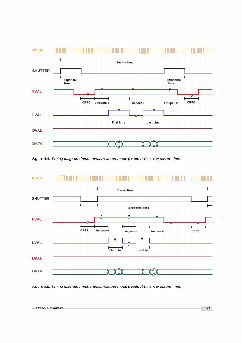
To achieve highest possible frame rates, the camera must be set to "Free-running mode" withsimultaneous readout. The camera continuously delivers images as fast as possible. Exposuretime of the next image can start during the readout time of the current image. The data isoutput on the rising edge of the pixel clock. The signals FRAME_VALID (FVAL) and LINE_VALID (LVAL)mask valid image information. The signal SHUTTER indicates the active integration phase of thesensor and is shown for clarity only.
56
P C L K
S H U T T E R
F V A L
L V A L
D V A L
D A T A
L i n e p a u s e L i n e p a u s e L i n e p a u s e
F i r s t L i n e L a s t L i n e
E x p o s u r eT i m e
F r a m e T i m e
C P R E
E x p o s u r eT i m e
C P R E
Figure 5.5: Timing diagram simultaneous readout mode (readout time > exposure time)
P C L K
S H U T T E R
F V A L
L V A L
D V A L
D A T A
L i n e p a u s e L i n e p a u s e L i n e p a u s e
F i r s t L i n e L a s t L i n e
F r a m e T i m e
C P R E
E x p o s u r e T i m e
C P R E
Figure 5.6: Timing diagram simultaneous readout mode (readout time < exposure time)
5.3 Read-out Timing 57

5 Hardware Interface
Frame time Frame time is the inverse of frame rate.
Exposure time Period during which the the pixels are integrating the incoming light.
PCLK Pixel clock on CameraLink interface.
SHUTTER Internal signal, shown only for clarity. Is ’high’ during the exposuretime.
FVAL (Frame Valid) Is ’high’ while the data of one whole frame are transferred.
LVAL (Line Valid) Is ’high’ while the data of one line are transferred. Example: To transferan image with 640x480 pixels, there are 480 LVAL within one FVAL activehigh period. One LVAL lasts 640 pixel clock cycles.
DVAL (Data Valid) Is ’high’ while data are valid.
DATA Transferred pixel values. Example: For a 100x100 pixel image, there are100 values transferred within one LVAL active high period, or 100*100values within one FVAL period.
Line pause Delay before the first line and after every following line when readingout the image data.
Table 5.4: Explanation of control and data signals used in the timing diagram
These terms will be used also in the timing diagrams of Section 5.4.
5.3.2 Constant Frame Rate Mode (CFR)
When the camera is in constant frame rate mode, the frame rate can be varied up to themaximum frame rate. Thus, fewer images can be acquired than determined by the frame time.When constant frame rate is switched off, the camera outputs images with maximum speed,depending on the exposure time and the read-out time. The frame rate depends directly onthe exposure time.
Constant Frame Rate mode is not available together with external trigger mode.
58

E x p o s u r e t i m e R e a d o u t t i m e
F r a m e t i m e
E x p o s u r e t i m e R e a d o u t t i m e
F r a m e t i m e
E x p o s u r e t i m e R e a d o u t t i m e
F r a m e t i m e
c f rt i m e E x p o s u r e t i m e R e a d o u t t i m e
F r a m e t i m e
c f rt i m e
C F R o f f
C F R o n
Figure 5.7: Constant Frame Rate with sequential readout mode
E x p o s u r e t i m e
R e a d o u t t i m e
F r a m e t i m e
E x p o s u r e t i m e
R e a d o u t t i m e
F r a m e t i m e
E x p o s u r e t i m e
R e a d o u t t i m e
F r a m e t i m e
E x p o s u r e t i m e
R e a d o u t t i m e
c f rt i m e
c f rt i m e
i d l e
i d l e
c f rt i m e
i d l e
c f rt i m ei d l e
F r a m e t i m e
C F R o f f
C F R o n
Figure 5.8: Constant Frame Rate with simultaneous readout mode (readout time > exposure time)
E x p o s u r e t i m e
R e a d o u t t i m e
F r a m e t i m e
E x p o s u r e t i m e
R e a d o u t t i m e
F r a m e t i m e
E x p o s u r e t i m e
R e a d o u t t i m e
F r a m e t i m e
E x p o s u r e t i m e
R e a d o u t t i m e
c f rt i m e
c f rt i m e
i d l e i d l e
i d l e c f rt i m e i d l e
c f rt i m e
F r a m e t i m e
C F R o f f
C F R o n
Figure 5.9: Constant Frame Rate with simultaneous readout mode (readout time < exposure time)
5.3 Read-out Timing 59
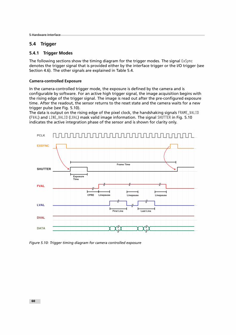
5 Hardware Interface
5.4 Trigger
5.4.1 Trigger Modes
The following sections show the timing diagram for the trigger modes. The signal ExSyncdenotes the trigger signal that is provided either by the interface trigger or the I/O trigger (seeSection 4.6). The other signals are explained in Table 5.4.
Camera-controlled Exposure
In the camera-controlled trigger mode, the exposure is defined by the camera and isconfigurable by software. For an active high trigger signal, the image acquisition begins withthe rising edge of the trigger signal. The image is read out after the pre-configured exposuretime. After the readout, the sensor returns to the reset state and the camera waits for a newtrigger pulse (see Fig. 5.10).The data is output on the rising edge of the pixel clock, the handshaking signals FRAME_VALID(FVAL) and LINE_VALID (LVAL) mask valid image information. The signal SHUTTER in Fig. 5.10indicates the active integration phase of the sensor and is shown for clarity only.
P C L K
S H U T T E R
F V A L
L V A L
D V A L
D A T A
L i n e p a u s e L i n e p a u s e L i n e p a u s e
F i r s t L i n e L a s t L i n e
E x p o s u r eT i m e
F r a m e T i m e
E X S Y N C
C P R E
Figure 5.10: Trigger timing diagram for camera controlled exposure
60
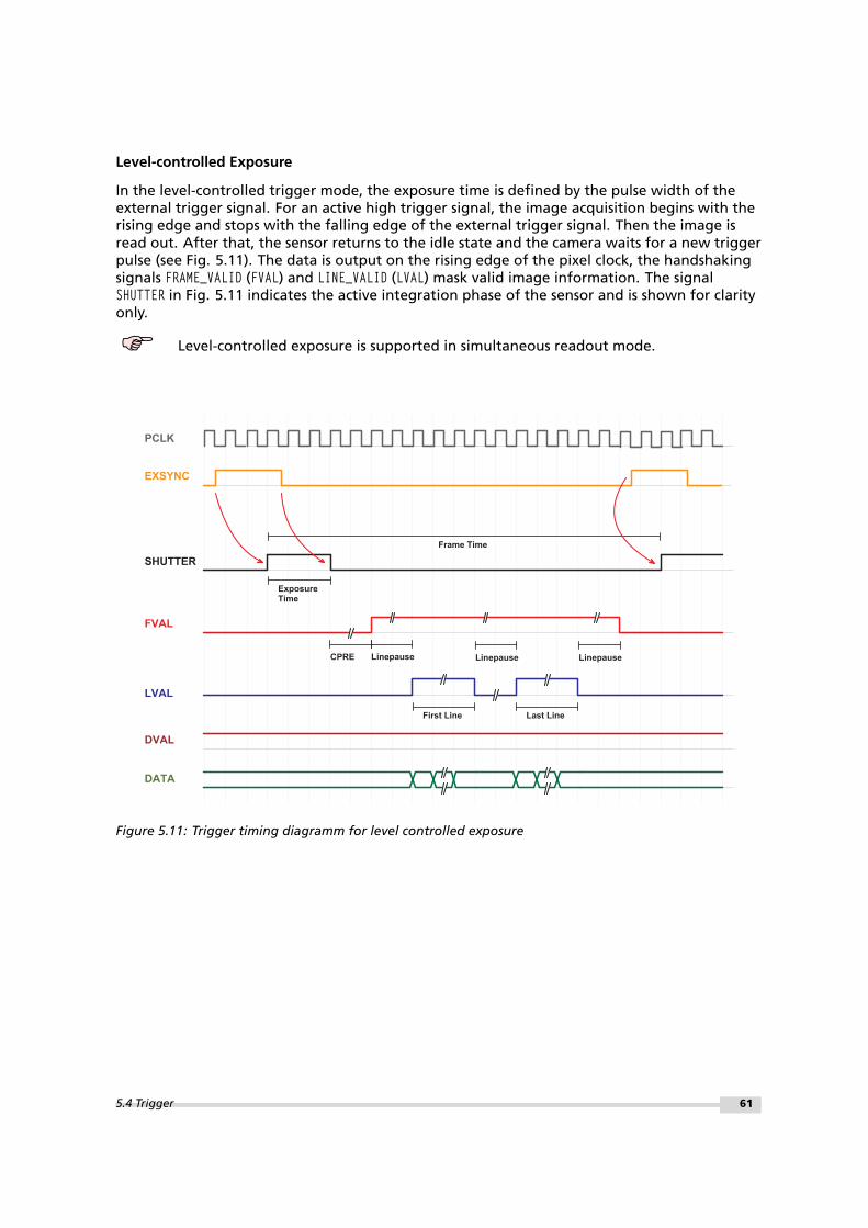
Level-controlled Exposure
In the level-controlled trigger mode, the exposure time is defined by the pulse width of theexternal trigger signal. For an active high trigger signal, the image acquisition begins with therising edge and stops with the falling edge of the external trigger signal. Then the image isread out. After that, the sensor returns to the idle state and the camera waits for a new triggerpulse (see Fig. 5.11). The data is output on the rising edge of the pixel clock, the handshakingsignals FRAME_VALID (FVAL) and LINE_VALID (LVAL) mask valid image information. The signalSHUTTER in Fig. 5.11 indicates the active integration phase of the sensor and is shown for clarityonly.
Level-controlled exposure is supported in simultaneous readout mode.
P C L K
S H U T T E R
F V A L
L V A L
D V A L
D A T A
L i n e p a u s e L i n e p a u s e L i n e p a u s e
F i r s t L i n e L a s t L i n e
E x p o s u r eT i m e
F r a m e T i m e
E X S Y N C
C P R E
Figure 5.11: Trigger timing diagramm for level controlled exposure
5.4 Trigger 61

5 Hardware Interface
5.4.2 Trigger Delay
The total delay between the trigger edge and the camera exposure consists of the delay in theframe grabber and the camera (Fig. 5.12). Usually, the delay in the frame grabber is relativelylarge to avoid accidental triggers caused by voltage spikes (see Fig. 5.13). The trigger can alsobe delayed by the property Trigger.Delay.
I n t e r f a c e T r i g g e rD A T A
PORT
APO
RT B
C a m e r a C a m e r a L i n k ® F r a m e G r a b b e r
I / O B o a r d
C C 1
I / O C o n t r o l
o p t oI / O
T r i g g e r S o u r c e1
2
3
14
T r i g g e r S o u r c eI / O T r i g g e r
T r i g g e r
Figure 5.12: Trigger Delay visualisation from the trigger source to the camera
1
2
3
t d _ F G
t j i t t e r
t d _ c a m e r a
T R I G G E R
E X S Y N C
I n t . E X S Y N C
S H U T T E R
T r i g g e r s o u r c e
F r a m e g r a b b e r
C a m e r a
C a m e r a
t d _ o p t o I / O
t d _ c a m e r a
4 C a m e r a o p t o I / O
C a m e r a
Figure 5.13: Timing Diagram for Trigger Delay
62

For the delay in the frame grabber, please ask your frame grabber manufacturer. The cameradelay consists of a constant trigger delay and a variable delay (jitter).
Trigger delay type Description
td−FG Trigger delay of the frame grabber, refer to frame grabber manual
tjitter Variable camera trigger delay (max. 25 ns)
td−camera Constant camera trigger delay (150 ns)
td−opto Variable trigger delay of opto coupler
Table 5.5: Trigger Delay
5.4 Trigger 63

5 Hardware Interface
64
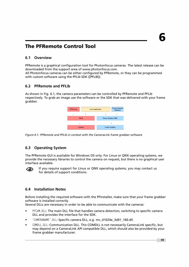
6The PFRemote Control Tool
6.1 Overview
PFRemote is a graphical configuration tool for Photonfocus cameras. The latest release can bedownloaded from the support area of www.photonfocus.com.All Photonfocus cameras can be either configured by PFRemote, or they can be programmedwith custom software using the PFLib SDK ([PFLIB]).
6.2 PFRemote and PFLib
As shown in Fig. 6.1, the camera parameters can be controlled by PFRemote and PFLibrespectively. To grab an image use the software or the SDK that was delivered with your framegrabber.
Figure 6.1: PFRemote and PFLib in context with the CameraLink frame grabber software
6.3 Operating System
The PFRemote GUI is available for Windows OS only. For Linux or QNX operating systems, weprovide the necessary libraries to control the camera on request, but there is no graphical userinterface available.
If you require support for Linux or QNX operating systems, you may contact usfor details of support conditions.
6.4 Installation Notes
Before installing the required software with the PFInstaller, make sure that your frame grabbersoftware is installed correctly.Several DLLs are necessary in order to be able to communicate with the cameras:
• PFCAM.DLL: The main DLL file that handles camera detection, switching to specific cameraDLL and provides the interface for the SDK.
• ’CAMERANAME’.DLL: Specific camera DLL, e.g. mv_d1024e_3d01_160.dll.
• COMDLL.DLL: Communication DLL. This COMDLL is not necessarily CameraLink specific, butmay depend on a CameraLink API compatible DLL, which should also be provided by yourframe grabber manufacturer.
65

6 The PFRemote Control Tool
• CLALLSERIAL.DLL: Interface to CameraLink frame grabber which supports the clallserial.dll.
• CLSER_USB.DLL: Interface to USB port.
More information about these DLLs is available in the SDK documentation [SW002].
6.5 Graphical User Interface (GUI)
PFRemote consists of a main window (Fig. 6.2) and a configuration dialog. In the main window,the camera port can be opened or closed, and log messages are displayed at the bottom. Theconfiguration dialog appears as a sub window as soon as a camera port was openedsuccessfully. In the sub window of PFRemote the user can configure the camera properties.The following sections describe the general structure of PFRemote.
6.5.1 Port Browser
On start, PFRemote displays a list of available communication ports in the main window.
Figure 6.2: PFRemote main window with PortBrowser and log messages
To open a camera on a specific port double click on the port name (e.g. USB). Alternativelyright click on the port name and choose Open & Configure.... The port is then queried for acompatible Photonfocus camera.In the PFRemote main window, there are two menus with the following entries available:
File Menu
Clear Log: Clears the log file buffer
Quit: Exit the program
Help Menu
About: Copyright notice and version information
Help F1: Invoke the online help (PFRemote documentation)
6.5.2 Ports, Device Initialization
After starting PFRemote, the main window as shown in Fig. 6.2 will appear. In the PortBrowserin the upper left corner you will see a list of supported ports.
66

Depending on the configuration, your port names may differ, and not every portmay be functional.
If your frame grabber supports clallserial.dll version 1.1 ( CameraLink compliantstandard Oct 2001), the name of the manufacturer is shown in the PortBrowser.
If your frame grabber supports clallserial.dll version 1.0 (CameraLink compliantstandard Oct 2000), the PortBrowser shows either the name of the dll or themanufacturer name or displays "Unknown".
If your frame grabber doesn’t support clallserial.dll, copy the clserXXXX.dll ofyour frame grabber in the PFRemote directory and rename it to clser.dll. ThePortBrowser will then indicate this DLL as "clser.dll at PFRemote directory".
After connecting the camera, the device can be opened with a double click on the port nameor by right-clicking on the port name and choosing Open & Configure. If the initialisation ofthe camera was successful, the configuration dialog will open. The device is closed whenPFRemote is closed. Alternatively, e.g. when connecting another camera or evaluation kit, thedevice can also be closed explicitely by right clicking on the port name and choosing Close.Make sure that the configuration dialog is closed prior to closing the port.
. Errors, warnings or other important activities are logged in a log window at thebottom of the main window.
If the device does not open, check the following:
• Is the power LED of the camera active? Do you get an image in the display software ofyour frame grabber?
• Verify all cable connections and the power supply.
• Check the communication LED of the camera: do you see some activity when you try toaccess the camera?
6.5 Graphical User Interface (GUI) 67

6 The PFRemote Control Tool
6.5.3 Main Buttons
The buttons on the right side of the configuration dialog store and reset the cameraconfiguration.
Figure 6.3: Main buttons
Reset: Reset the camera and load the default configuration.
Store as defaults: Store the current configuration in the camera flash memory as the defaultconfiguration. After a reset, the camera will load this configuration by default.
Settings file - File Load: Load a stored configuration from a file.
Settings file - File Save: Save current configuration to a file.
Factory Reset: Reset camera and reset the configuration to the factory defaults.
6.6 Device Properties
Cameras or sensor devices are generally addressed as ’device’ in this software. These deviceshave properties that are accessed by a property name. These property names are translatedinto register accesses on the driver DLL. The property names are reflected in the GUI as far aspracticable. A property name normally has a special mark up throughout this document, forexample: ExposureTime. Some properties are grouped into a structure whose member isaccessed via dot notation, e.g. Window.X (for the start X value of a region of interest). Whenchanging a property, the property name can always be seen in the log window of the mainprogram window.
68

7Graphical User Interface (GUI)
7.1 MV-D1024E-3D01-160
This section describes the parameters of the following cameras.
• MV-D1024E-3D01-160-CL, CameraLink interface
The following sections are grouped according to the tabs in the configuration dialog.
Figure 7.1: MV-D1024E-3D01-160 frame rate and average value
Frame Rate [fps :] Shows the actual frame rate of the camera in frames per second.
Update: To update the value of the frame rate, click on this button.
Average Value: Greyscale average of the actual image. This value is in 12bit (0...4095).
Update: To update the value of the average, click on this button.
69

7 Graphical User Interface (GUI)
7.1.1 Exposure
This tab contains exposure settings.
Figure 7.2: MV-D1024E-3D01-160 exposure panel
Exposure
Exposure time [ms :] Configure the exposure time in milliseconds.
Constant Frame Rate: When the Constant Frame Rate (CFR) is switched on, the frame rate(number of frames per second) can be varied from almost 0 up to the maximum framerate. Thus, fewer images can be acquired than would otherwise be possible. WhenConstant Frame Rate is switched off, the camera delivers images as fast as possible,depending on the exposure time and the read-out time.
Frame time [ms :] Configure the frame time in milliseconds. Only available if Constant FrameRate is enabled. The minimum frame time depends on the exposure time and readouttime.
Information
The Information properties provide information about the acquired images.
Image Counter: The image counter is a 24 bit real-time counter and is incremented by 1 forevery new image.
Missed Trigger Counter: This is a counter for trigger pulses that were blocked because thetrigger pulse was received during image exposure or readout. In free-running mode itcounts all pulses received from interface trigger or from I/O trigger interface.
Status Line: The status line replaces the last line of an image with image information.
To update the value of the information properties, click on the Update-Button; to reset theproperties, click on the Reset-Button.
70
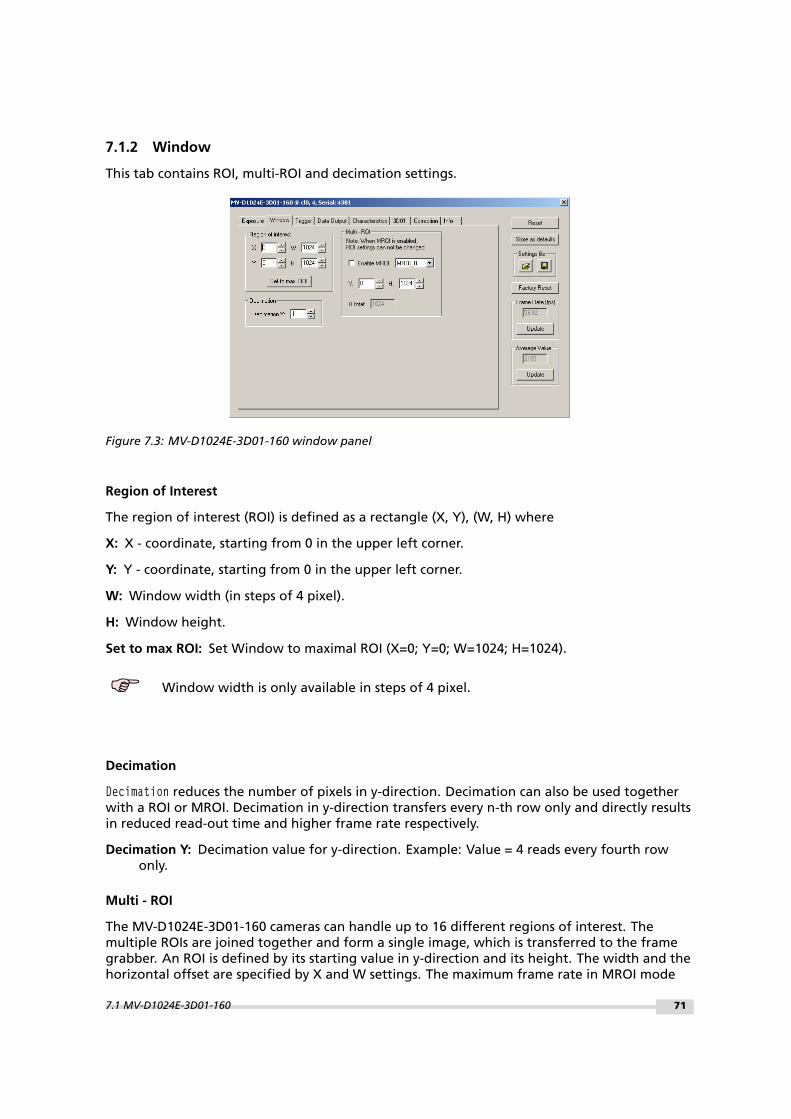
7.1.2 Window
This tab contains ROI, multi-ROI and decimation settings.
Figure 7.3: MV-D1024E-3D01-160 window panel
Region of Interest
The region of interest (ROI) is defined as a rectangle (X, Y), (W, H) where
X: X - coordinate, starting from 0 in the upper left corner.
Y: Y - coordinate, starting from 0 in the upper left corner.
W: Window width (in steps of 4 pixel).
H: Window height.
Set to max ROI: Set Window to maximal ROI (X=0; Y=0; W=1024; H=1024).
Window width is only available in steps of 4 pixel.
Decimation
Decimation reduces the number of pixels in y-direction. Decimation can also be used togetherwith a ROI or MROI. Decimation in y-direction transfers every n-th row only and directly resultsin reduced read-out time and higher frame rate respectively.
Decimation Y: Decimation value for y-direction. Example: Value = 4 reads every fourth rowonly.
Multi - ROI
The MV-D1024E-3D01-160 cameras can handle up to 16 different regions of interest. Themultiple ROIs are joined together and form a single image, which is transferred to the framegrabber. An ROI is defined by its starting value in y-direction and its height. The width and thehorizontal offset are specified by X and W settings. The maximum frame rate in MROI mode
7.1 MV-D1024E-3D01-160 71

7 Graphical User Interface (GUI)
depends on the number of rows and columns being read out. Overlapping ROIs are allowed,and the total height may exceed 1024 rows.
Enable MROI: Enable MROI. If MROI is enabled, the ROI and MROI settings cannot be changed.
MROI_X: Select one of the MROI settings.
Y: Y - coordinate of the selected MROI. If Y is set to 1023, this and all further MROI settings willbe ignored.
H: Height of the selected MROI.
H tot: Shows the sum of all MROIs as the total image height.
After changing a property, always press Enter in order to make the change active.
72
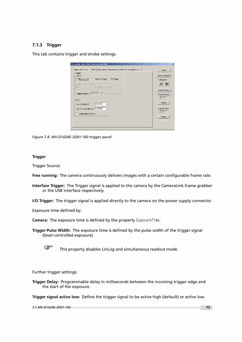
7.1.3 Trigger
This tab contains trigger and strobe settings.
Figure 7.4: MV-D1024E-3D01-160 trigger panel
Trigger
Trigger Source:
Free running: The camera continuously delivers images with a certain configurable frame rate.
Interface Trigger: The Trigger signal is applied to the camera by the CameraLink frame grabberor the USB interface respectively.
I/O Trigger: The trigger signal is applied directly to the camera on the power supply connector.
Exposure time defined by:
Camera: The exposure time is defined by the property ExposureTime.
Trigger Pulse Width: The exposure time is defined by the pulse width of the trigger signal(level-controlled exposure).
This property disables LinLog and simultaneous readout mode.
Further trigger settings:
Trigger Delay: Programmable delay in milliseconds between the incoming trigger edge andthe start of the exposure.
Trigger signal active low: Define the trigger signal to be active high (default) or active low.
7.1 MV-D1024E-3D01-160 73

7 Graphical User Interface (GUI)
Strobe
The camera generates a strobe output signal that can be used to trigger a strobe. The delay,pulse width and polarity can be defined by software. To turn off strobe output, setStrobePulseWidth to 0.
Strobe Delay [ms :] Delay in milliseconds from the input trigger edge to the rising edge of thestrobe output signal.
Strobe Pulse Width [ms :] The pulse width of the strobe trigger in milliseconds.
Strobe signal active low: Define the strobe output to be active high (default) or active low.
74
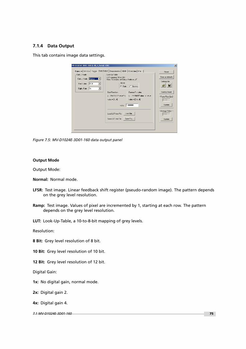
7.1.4 Data Output
This tab contains image data settings.
Figure 7.5: MV-D1024E-3D01-160 data output panel
Output Mode
Output Mode:
Normal: Normal mode.
LFSR: Test image. Linear feedback shift register (pseudo-random image). The pattern dependson the grey level resolution.
Ramp: Test image. Values of pixel are incremented by 1, starting at each row. The patterndepends on the grey level resolution.
LUT: Look-Up-Table, a 10-to-8-bit mapping of grey levels.
Resolution:
8 Bit: Grey level resolution of 8 bit.
10 Bit: Grey level resolution of 10 bit.
12 Bit: Grey level resolution of 12 bit.
Digital Gain:
1x: No digital gain, normal mode.
2x: Digital gain 2.
4x: Digital gain 4.
7.1 MV-D1024E-3D01-160 75
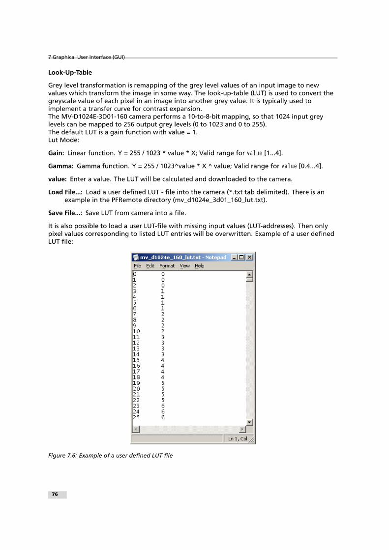
7 Graphical User Interface (GUI)
Look-Up-Table
Grey level transformation is remapping of the grey level values of an input image to newvalues which transform the image in some way. The look-up-table (LUT) is used to convert thegreyscale value of each pixel in an image into another grey value. It is typically used toimplement a transfer curve for contrast expansion.The MV-D1024E-3D01-160 camera performs a 10-to-8-bit mapping, so that 1024 input greylevels can be mapped to 256 output grey levels (0 to 1023 and 0 to 255).The default LUT is a gain function with value = 1.Lut Mode:
Gain: Linear function. Y = 255 / 1023 * value * X; Valid range for value [1...4].
Gamma: Gamma function. Y = 255 / 1023^value * X ^ value; Valid range for value [0.4...4].
value: Enter a value. The LUT will be calculated and downloaded to the camera.
Load File...: Load a user defined LUT - file into the camera (*.txt tab delimited). There is anexample in the PFRemote directory (mv_d1024e_3d01_160_lut.txt).
Save File...: Save LUT from camera into a file.
It is also possible to load a user LUT-file with missing input values (LUT-addresses). Then onlypixel values corresponding to listed LUT entries will be overwritten. Example of a user definedLUT file:
Figure 7.6: Example of a user defined LUT file
76
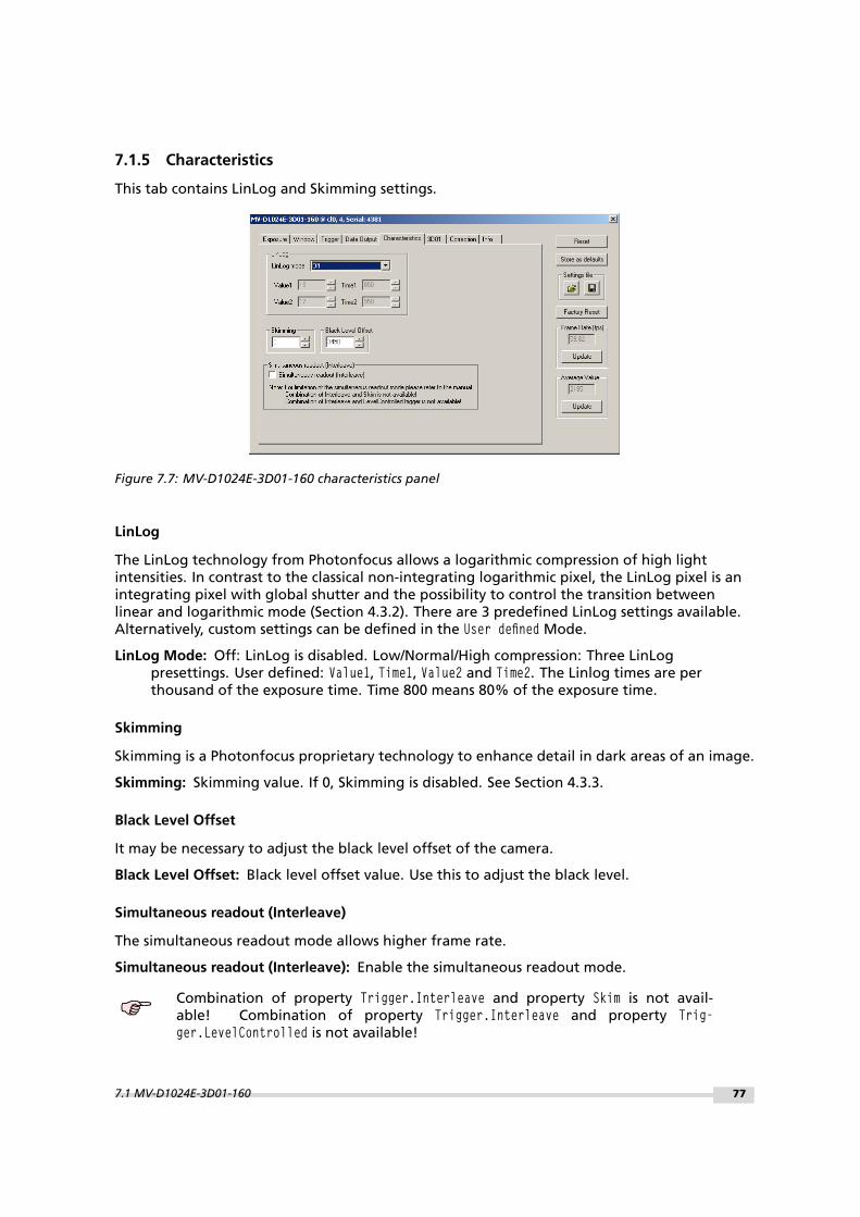
7.1.5 Characteristics
This tab contains LinLog and Skimming settings.
Figure 7.7: MV-D1024E-3D01-160 characteristics panel
LinLog
The LinLog technology from Photonfocus allows a logarithmic compression of high lightintensities. In contrast to the classical non-integrating logarithmic pixel, the LinLog pixel is anintegrating pixel with global shutter and the possibility to control the transition betweenlinear and logarithmic mode (Section 4.3.2). There are 3 predefined LinLog settings available.Alternatively, custom settings can be defined in the User defined Mode.
LinLog Mode: Off: LinLog is disabled. Low/Normal/High compression: Three LinLogpresettings. User defined: Value1, Time1, Value2 and Time2. The Linlog times are perthousand of the exposure time. Time 800 means 80% of the exposure time.
Skimming
Skimming is a Photonfocus proprietary technology to enhance detail in dark areas of an image.
Skimming: Skimming value. If 0, Skimming is disabled. See Section 4.3.3.
Black Level Offset
It may be necessary to adjust the black level offset of the camera.
Black Level Offset: Black level offset value. Use this to adjust the black level.
Simultaneous readout (Interleave)
The simultaneous readout mode allows higher frame rate.
Simultaneous readout (Interleave): Enable the simultaneous readout mode.
Combination of property Trigger.Interleave and property Skim is not avail-able! Combination of property Trigger.Interleave and property Trig-ger.LevelControlled is not available!
7.1 MV-D1024E-3D01-160 77
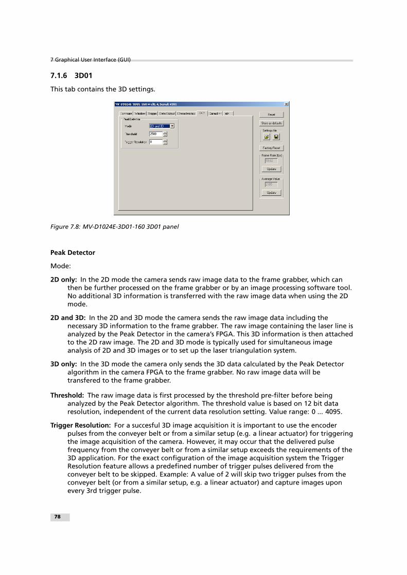
7 Graphical User Interface (GUI)
7.1.6 3D01
This tab contains the 3D settings.
Figure 7.8: MV-D1024E-3D01-160 3D01 panel
Peak Detector
Mode:
2D only: In the 2D mode the camera sends raw image data to the frame grabber, which canthen be further processed on the frame grabber or by an image processing software tool.No additional 3D information is transferred with the raw image data when using the 2Dmode.
2D and 3D: In the 2D and 3D mode the camera sends the raw image data including thenecessary 3D information to the frame grabber. The raw image containing the laser line isanalyzed by the Peak Detector in the camera’s FPGA. This 3D information is then attachedto the 2D raw image. The 2D and 3D mode is typically used for simultaneous imageanalysis of 2D and 3D images or to set up the laser triangulation system.
3D only: In the 3D mode the camera only sends the 3D data calculated by the Peak Detectoralgorithm in the camera FPGA to the frame grabber. No raw image data will betransfered to the frame grabber.
Threshold: The raw image data is first processed by the threshold pre-filter before beinganalyzed by the Peak Detector algorithm. The threshold value is based on 12 bit dataresolution, independent of the current data resolution setting. Value range: 0 ... 4095.
Trigger Resolution: For a succesful 3D image acquisition it is important to use the encoderpulses from the conveyer belt or from a similar setup (e.g. a linear actuator) for triggeringthe image acquisition of the camera. However, it may occur that the delivered pulsefrequency from the conveyer belt or from a similar setup exceeds the requirements of the3D application. For the exact configuration of the image acquisition system the TriggerResolution feature allows a predefined number of trigger pulses delivered from theconveyer belt to be skipped. Example: A value of 2 will skip two trigger pulses from theconveyer belt (or from a similar setup, e.g. a linear actuator) and capture images uponevery 3rd trigger pulse.
78

7.1.7 Correction
This tab contains correction settings.
Figure 7.9: MV-D1024E-3D01-160 correction panel
Correction Mode
This camera has image pre-processing features, that compensate for non-uniformities causedby the sensor, the lens or the illumination.
Off: No correction.
Offset: Activate offset correction
Offset + Hotpixel: Activate offset and hot pixel correction.
Hotpixel: Activate hot pixel correction.
Offset + Gain: Activate offset and gain correction.
Offset + Gain + Hotpixel: Activate offset, gain and hot pixel correction.
Calibration
Offset (FPN), Hotpixel Correction: The offset correction is based on a black reference image,which is taken at no illumination (e.g. lens aperture completely closed). The blackreference image contains the fixed-pattern noise of the sensor, which can be subtractedfrom the live images in order to minimize the static noise. Close the lens of the camera.Click on the Validation button. If the Set Black Ref - button is still inactive, the average ofthe image is out of range. Change to panel Charateristics and change the PropertyBlackLevelOffset until the average of the image is between 160 and 400DN. Click againon the Validation button and then on the Set Black Ref Button.
If only offset and hot pixel correction is needed it is not necessary to calibrate agrey image (see Calculate).
7.1 MV-D1024E-3D01-160 79

7 Graphical User Interface (GUI)
Gain Correction: The gain correction is based on a grey reference image, which is taken atuniform illumination to give an image with a mid grey level.
Gain correction is not a trivial feature. The quality of the grey reference imageis crucial for proper gain correction.
Produce a grey image with an average between 2200 and 3600DN. Click on the Validationbutton to check the average. If the average is in range, the Set Grey Ref button is active.
Calculate: Calculate the correction values into the camera RAM. To make the correction valuespermanent, use the ’Save to Flash’ button.
Save to Flash: Save the current correction values to the internal flash memory.
This will overwrite the factory presets.
80

7.1.8 Info
This panel shows camera specific information such as type code, serial number and firmwarerevision of the FPGA and microcontroller and the description of the camera interface.
Figure 7.10: MV-D1024E-3D01-160 info panel
Typecode: Type code of the connected camera.
Serial: Serial number of the connected camera.
FPGA Sensor Revision: Firmware revision of built-in Sensor FPGA of the connected camera.
FPGA ADC Revision: Firmware revision of built-in ADC FPGA of the connected camera.
uC Revision: Firmware revision of built-in microcontroller of the connected camera.
Interface: Description of the camera interface.
For any support requests, please enclose the information provided on this tab.
7.1 MV-D1024E-3D01-160 81

7 Graphical User Interface (GUI)
82
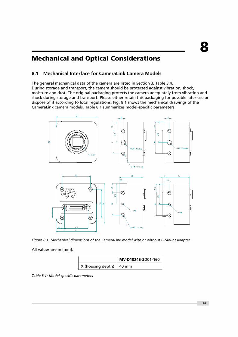
8Mechanical and Optical Considerations
8.1 Mechanical Interface for CameraLink Camera Models
The general mechanical data of the camera are listed in Section 3, Table 3.4.During storage and transport, the camera should be protected against vibration, shock,moisture and dust. The original packaging protects the camera adequately from vibration andshock during storage and transport. Please either retain this packaging for possible later use ordispose of it according to local regulations. Fig. 8.1 shows the mechanical drawings of theCameraLink camera models. Table 8.1 summarizes model-specific parameters.
Figure 8.1: Mechanical dimensions of the CameraLink model with or without C-Mount adapter
All values are in [mm].
MV-D1024E-3D01-160
X (housing depth) 40 mm
Table 8.1: Model-specific parameters
83
8 Mechanical and Optical Considerations
8.2 Optical Interface
8.2.1 Cleaning the Sensor
The sensor is part of the optical path and should be handled like other optical components:with extreme care.Dust can obscure pixels, producing dark patches in the images captured. Dust is most visiblewhen the illumination is collimated. Dark patches caused by dust or dirt shift position as theangle of illumination changes. Dust is normally not visible when the sensor is positioned at theexit port of an integrating sphere, where the illumination is diffuse.
1. The camera should only be cleaned in ESD-safe areas by ESD-trained personnel using wriststraps. Ideally, the sensor should be cleaned in a clean environment. Otherwise, in dustyenvironments, the sensor will immediately become dirty again after cleaning.
2. Use a high quality, low pressure air duster (e.g. Electrolube EAD400D, pure compressedinert gas, www.electrolube.com) to blow off loose particles. This step alone is usuallysufficient to clean the sensor of the most common contaminants.
Workshop air supply is not appropriate and may cause permanent damage tothe sensor.
3. If further cleaning is required, use a suitable lens wiper or Q-Tip moistened with anappropriate cleaning fluid to wipe the sensor surface as described below. Examples ofsuitable lens cleaning materials are given in Table 8.2. Cleaning materials must beESD-safe, lint-free and free from particles that may scratch the sensor surface.
Do not use ordinary cotton buds. These do not fulfil the above requirements andpermanent damage to the sensor may result.
4. Wipe the sensor carefully and slowly. First remove coarse particles and dirt from thesensor using Q-Tips soaked in 2-propanol, applying as little pressure as possible. Using amethod similar to that used for cleaning optical surfaces, clean the sensor by starting atany corner of the sensor and working towards the opposite corner. Finally, repeat theprocedure with methanol to remove streaks. It is imperative that no pressure be appliedto the surface of the sensor or to the black globe-top material (if present) surrounding theoptically active surface during the cleaning process.
84

Product Supplier Remark
EAD400D Airduster Electrolube, UK www.electrolube.com
Anticon Gold 9"x 9" Wiper Milliken, USA ESD safe and suitable forclass 100 environments.www.milliken.com
TX4025 Wiper Texwipe www.texwipe.com
Transplex Swab Texwipe
Small Q-Tips SWABSBB-003
Q-tips Hans J. Michael GmbH,Germany
www.hjm.de
Large Q-Tips SWABSCA-003
Q-tips Hans J. Michael GmbH,Germany
Point Slim HUBY-340 Q-tips Hans J. Michael GmbH,Germany
Methanol Fluid Johnson Matthey GmbH,Germany
Semiconductor Grade99.9% min (Assay),Merck 12,6024, UN1230,slightly flammable andpoisonous.www.alfa-chemcat.com
2-Propanol(Iso-Propanol)
Fluid Johnson Matthey GmbH,Germany
Semiconductor Grade99.5% min (Assay) Merck12,5227, UN1219,slightly flammable.www.alfa-chemcat.com
Table 8.2: Recommended materials for sensor cleaning
For cleaning the sensor, Photonfocus recommends the products available from the suppliers aslisted in Table 8.2.
. Cleaning tools (except chemicals) can be purchased from Photonfocus(www.photonfocus.com).
.
8.2 Optical Interface 85
8 Mechanical and Optical Considerations
8.3 Compliance
C E C o m p l i a n c e S t a t e m e n t
M V - D 1 0 2 4 - 2 8 - C L - 1 0 , M V - D 1 0 2 4 - 8 0 - C L - 8 , M V - D 1 0 2 4 - 1 6 0 - C L - 8M V - D 7 5 2 - 2 8 - C L - 1 0 , M V - D 7 5 2 - 8 0 - C L - 8 , M V - D 7 5 2 - 1 6 0 - C L - 8M V - D 6 4 0 - 3 3 - C L - 1 0 , M V - D 6 4 0 - 6 6 - C L - 1 0 , M V - D 6 4 0 - 4 8 - U 2 - 8M V - D 6 4 0 C - 3 3 - C L - 1 0 , M V - D 6 4 0 C - 6 6 - C L - 1 0 , M V - D 6 4 0 C - 4 8 - U 2 - 8M V - D 1 0 2 4 E - 4 0 , M V - D 7 5 2 E - 4 0 , M V - D 7 5 0 E - 2 0 ( C a m e r a L i n k a n dU S B 2 . 0 M o d e l s ) , M V - D 1 0 2 4 E - 8 0 , M V - D 1 0 2 4 E - 1 6 0M V - D 1 0 2 4 E - 3 D 0 1 - 1 6 0M V 2 - D 1 2 8 0 - 6 4 0 - C L - 8S M 2 - D 1 0 2 4 - 8 0 / V i s i o n C a m P SD S 1 - D 1 0 2 4 - 4 0 - C L , D S 1 - D 1 0 2 4 - 4 0 - U 2 ,D S 1 - D 1 0 2 4 - 8 0 - C L , D S 1 - D 1 0 2 4 - 1 6 0 - C LD S 1 - D 1 3 1 2 - 1 6 0 - C L , M V 1 - D 1 3 1 2 - 1 6 0 - C LD i g i p e a t e r C L B 2 6
a r e i n c o m p l i a n c e w i t h t h e b e l o w m e n t i o n e d s t a n d a r d s a c c o r d i n g t ot h e p r o v i s i o n s o f E u r o p e a n S t a n d a r d s D i r e c t i v e s :
W e ,
P h o t o n f o c u s A G ,C H - 8 8 5 3 L a c h e n , S w i t z e r l a n dd e c l a r e u n d e r o u r s o l e r e s p o n s i b i l i t y t h a t t h e f o l l o w i n g p r o d u c t s
E N 6 1 0 0 0 - 6 - 3 : 2 0 0 1E N 6 1 0 0 0 - 6 - 2 : 2 0 0 1E N 6 1 0 0 0 - 4 - 6 : 1 9 9 6E N 6 1 0 0 0 - 4 - 4 : 1 9 9 6E N 6 1 0 0 0 - 4 - 3 : 1 9 9 6E N 6 1 0 0 0 - 4 - 2 : 1 9 9 5E N 5 5 0 2 2 : 1 9 9 4
P h o t o n f o c u s A G , O c t o b e r 2 0 0 8Figure 8.2: CE Compliance Statement
86
9Warranty
The manufacturer alone reserves the right to recognize warranty claims.
9.1 Warranty Terms
The manufacturer warrants to distributor and end customer that for a period of two yearsfrom the date of the shipment from manufacturer or distributor to end customer (the"Warranty Period") that:
• the product will substantially conform to the specifications set forth in the applicabledocumentation published by the manufacturer and accompanying said product, and
• the product shall be free from defects in materials and workmanship under normal use.
The distributor shall not make or pass on to any party any warranty or representation onbehalf of the manufacturer other than or inconsistent with the above limited warranty set.
9.2 Warranty Claim
The above warranty does not apply to any product that has been modified or al-tered by any party other than manufacturer, or for any defects caused by any useof the product in a manner for which it was not designed, or by the negligenceof any party other than manufacturer.
87

9 Warranty
88
10References
All referenced documents can be downloaded from our website at www.photonfocus.com.
CL CameraLink®Specification, Rev. 1.1, January 2004
SW002 PFLib Documentation, Photonfocus, August 2005
AN001 Application Note "LinLog®", Photonfocus, December 2002
AN024 Application Note "LinLog®- Principle and Practical Example", Photonfocus, March 2005
AN007 Application Note "Camera Acquisition Modes", Photonfocus, March 2004
AN010 Application Note "Camera Clock Concepts", Photonfocus, July 2004
AN021 Application Note "CameraLink®", Photonfocus, July 2004
AN026 Application Note "LFSR Test Images", Photonfocus, September 2005
AN028 Application Note "3D System Configuration", Photonfocus, August 2008
AN030 Application Note "LinLog®Parameter Optimization Strategies", February 2009
MAN040 User Manual "PF 3D Suite", Photonfocus, October 2008
89

10 References
90

APinouts
A.1 Power Supply for CameraLink Camera Models
The power supply plugs are available from Binder connectors at www.binder-connector.de.
It is extremely important that you apply the appropriate voltages to your camera.Incorrect voltages will damage or destroy the camera.
A suitable power supply is available from Photonfocus.
Figure A.1: Power connector assembly
A.1.1 Power Supply Connector
Table A.1 summarizes the order codes for the 7-pole Binder connector. Table A.2 gives the pinassignment for the power supply connector with included I/O ports.
Connector Type Order Code
7-pole, plastic 99-0421-00-07
7-pole, metal 99-0421-10-07
Table A.1: Power supply connectors (Binder subminiature series 712)
91

A Pinouts
12
34
5
67
Figure A.2: Power supply plug, 7-pole (rear view of plug, solder side)
Pin I/O Type Name Description
1 PWR VDD +12 V DC (± 10%)
2 PWR GND Ground
3 O RESERVED Do not connect
4 PWR STROBE-VDD +5 .. +15 V DC
5 O STROBE Strobe control (opto-isolated)
6 I TRIGGER External trigger (opto-isolated), +5 .. +15V DC
7 PWR GROUND Signal ground (for opto-isolated strobe signal)
Table A.2: Power supply plug pin assignment
A.2 CameraLink Connector for CameraLink Camera Models
The pinout for the CameraLink 26 pin, 0.05" Mini D-Ribbon (MDR) connector is according tothe CameraLink standard ([CL]) and is listed here for reference only (see Table A.3). Thedrawing of the CameraLink cable plug is shown in Fig. A.3. CameraLink cables can bepurchased from Photonfocus directly (www.photonfocus.com).
21 3 4 5 6 7 8 9 1 0 1 1 1 2 1 3
1 4 1 5 1 6 1 7 1 8 1 9 2 0 2 1 2 2 2 3 2 4 2 5 2 6
Figure A.3: CameraLink cable 3M MDR-26 plug (both ends)
.
92

PIN IO Name Description
1 PW INNER SHIELD Inner Shield
2 O N_XD0 Negative LVDS Output, CameraLink Data D0
3 O N_XD1 Negative LVDS Output, CameraLink Data D1
4 O N_XD2 Negative LVDS Output, CameraLink Data D2
5 O N_XCLK Negative LVDS Output, CameraLink Clock
6 O N_XD3 Negative LVDS Output, CameraLink Data D3
7 I P_SERTOCAM Positive LVDS Input, Serial Communication to the camera
8 O N_SERTOFG Negative LVDS Output, Serial Communication from the camera
9 I N_CC1 Negative LVDS Input, Camera Control 1 (CC1)
10 I N_CC2 Positive LVDS Input, Camera Control 2 (CC2)
11 I N_CC3 Negative LVDS Input, Camera Control 3 (CC3)
12 I P_CC4 Positive LVDS Input, Camera Control 4 (CC4)
13 PW INNER SHIELD Inner Shield
14 PW INNER SHIELD Inner Shield
15 O P_XD0 Positive LVDS Output, CameraLink Data D0
16 O P_XD1 Positive LVDS Output, CameraLink Data D1
17 O P_XD2 Positive LVDS Output, CameraLink Data D2
18 O P_XCLK Positive LVDS Output, CameraLink Clock
19 O P_XD3 Positive LVDS Output, CameraLink Data D3
20 I N_SERTOCAM Negative LVDS Input, Serial Communication to the camera
21 O P_SERTOFG Positive LVDS Output, Serial Communication from the camera
22 I P_CC1 Positive LVDS Input, Camera Control 1 (CC1)
23 I N_CC2 Negative LVDS Input, Camera Control 2 (CC2)
24 I P_CC3 Positive LVDS Input, Camera Control 3 (CC3)
25 I N_CC4 Negative LVDS Input, Camera Control 4 (CC4)
26 PW INNER SHIELD Inner Shield
S PW SHIELD Shield
Table A.3: Pinout CameraLink connector
.
A.2 CameraLink Connector for CameraLink Camera Models 93

A Pinouts
94
BRevision History
Revision Date Changes
1.0 August 2008 First release
1.1 April 2009 Incorporation of improved width calculation method
3D data output placed on the 8 LSB of the grey value
Modified format of width indicator, comprising
an integer part and a fractional part
95


