This content has been downloaded from IOPscience. Please scroll down to see the full text. Download details: IP Address: 83.48.67.242 This content was downloaded on 07/09/2017 at 08:53 Please note that terms and conditions apply. Mapping the electrical properties of large-area graphene View the table of contents for this issue, or go to the journal homepage for more 2017 2D Mater. 4 042003 (http://iopscience.iop.org/2053-1583/4/4/042003) Home Search Collections Journals About Contact us My IOPscience You may also be interested in: A review of the electrical properties of semiconductor nanowires: Insights gained from terahertz conductivity spectroscopy Hannah J Joyce, Jessica L Boland, Christopher L Davies et al. Electronic properties of graphene: a perspective from scanning tunneling microscopy and magnetotransport Eva Y Andrei, Guohong Li and Xu Du Combining graphene with silicon carbide: synthesis and properties – a review Ivan Shtepliuk, Volodymyr Khranovskyy and Rositsa Yakimova Engineering metallic nanostructures for plasmonics and nanophotonics Nathan C Lindquist, Prashant Nagpal, Kevin M McPeak et al. Engineering electrical properties of graphene: chemical approaches Yong-Jin Kim, Yuna Kim, Konstantin Novoselov et al. Advances in graphene–based optoelectronics, plasmonics and photonics Bich Ha Nguyen and Van Hieu Nguyen Imaging with terahertz radiation Wai Lam Chan, Jason Deibel and Daniel M Mittleman
Transcript
This content has been downloaded from IOPscience. Please scroll down to see the full text.
Download details:
IP Address: 83.48.67.242
This content was downloaded on 07/09/2017 at 08:53
Please note that terms and conditions apply.
Mapping the electrical properties of large-area graphene
View the table of contents for this issue, or go to the journal homepage for more
2017 2D Mater. 4 042003
(http://iopscience.iop.org/2053-1583/4/4/042003)
Home Search Collections Journals About Contact us My IOPscience
You may also be interested in:
A review of the electrical properties of semiconductor nanowires: Insights gained from terahertz
conductivity spectroscopy
Hannah J Joyce, Jessica L Boland, Christopher L Davies et al.
Electronic properties of graphene: a perspective from scanning tunneling microscopy and
magnetotransport
Eva Y Andrei, Guohong Li and Xu Du
Combining graphene with silicon carbide: synthesis and properties – a review
Ivan Shtepliuk, Volodymyr Khranovskyy and Rositsa Yakimova
Engineering metallic nanostructures for plasmonics and nanophotonics
Nathan C Lindquist, Prashant Nagpal, Kevin M McPeak et al.
Engineering electrical properties of graphene: chemical approaches
Yong-Jin Kim, Yuna Kim, Konstantin Novoselov et al.
Advances in graphene–based optoelectronics, plasmonics and photonics
In 2006 the price of commercially available single layer graphene was 1 euro per µm2. More than a decade after, the price is approaching 1 euro per cm2, representing roughly a factor of 108 decrease of the price per area. This development has been made possible due to development of the chemical vapor deposition (CVD) process for synthesis of graphene on copper foils. While high quality graphite-derived graphene products are produced in various ways including oxidation and reduction of graphite [1, 2] and liquid exfoliation [3, 4], CVD synthesis of graphene on catalytic metals is by far the most successful, widespread, and scalable
means to produce continuous, high quality graphene films [5]. Epitaxial graphene synthesized by high-temperature sublimation of silicon atoms from a silicon carbide wafer also shows promise [6, 7].
CVD synthesis of macroscopic graphene films has evolved from early pioneering works, with few-layer graphene growth on nickel catalyst demonstrated by several authors [8, 9] followed by demonstration of large-area single-layer graphene synthesis on copper foil by Ruoff and colleagues [10]. Soon after, a roll-to-roll based process showed that single-layer graphene can indeed be fabricated and transferred to essentially square-meter sized substrates [11]. Numerous other roll-to-roll systems have been developed [12, 13], with
Mapping the electrical properties of large-area graphene
Peter Bøggild1 , David M A Mackenzie1, Patrick R Whelan1, Dirch H Petersen1, Jonas Due Buron1, Amaia Zurutuza2, John Gallop3, Ling Hao3 and Peter U Jepsen4
1 Department of Micro- and Nanotechnology, Center for Nanostructured Graphene (CNG), Technical University of Denmark, Ørsteds Plads 345C, Kongens Lyngby, 2800, Denmark
2 Graphenea S.A., Avenida de Tolosa, 76, 20018—Donostia/San Sebastián, Spain3 National Physical Laboratory, Quantum Detection Group, Teddington, TW11 0LW, United Kingdom4 Department of Photonics Engineering, Center for Nanostructured Graphene (CNG), Technical University of Denmark,
AbstractThe significant progress in terms of fabricating large-area graphene films for transparent electrodes, barriers, electronics, telecommunication and other applications has not yet been accompanied by efficient methods for characterizing the electrical properties of large-area graphene. While in the early prototyping as well as research and development phases, electrical test devices created by conventional lithography have provided adequate insights, this approach is becoming increasingly problematic due to complications such as irreversible damage to the original graphene film, contamination, and a high measurement effort per device. In this topical review, we provide a comprehensive overview of the issues that need to be addressed by any large-area characterisation method for electrical key performance indicators, with emphasis on electrical uniformity and on how this can be used to provide a more accurate analysis of the graphene film. We review and compare three different, but complementary approaches that rely either on fixed contacts (dry laser lithography), movable contacts (micro four point probes) and non-contact (terahertz time-domain spectroscopy) between the probe and the graphene film, all of which have been optimized for maximal throughput and accuracy, and minimal damage to the graphene film. Of these three, the main emphasis is on THz time-domain spectroscopy, which is non-destructive, highly accurate and allows both conductivity, carrier density and carrier mobility to be mapped across arbitrarily large areas at rates that by far exceed any other known method. We also detail how the THz conductivity spectra give insights on the scattering mechanisms, and through that, the microstructure of graphene films subject to different growth and transfer processes. The perspectives for upscaling to realistic production environments are discussed.
TOPICAL REVIEW2017
Original content from this work may be used under the terms of the Creative Commons Attribution 3.0 licence.
Any further distribution of this work must maintain attribution to the author(s) and the title of the work, journal citation and DOI.
Kobayashi and colleagues demonstrating 100 meter long continuous graphene sheets transferred to a PET polymer substrate. Other large-area graphene strate-gies include folded or rolled up copper substrates [14]. Recently, several manufacturers of CVD equipment have launched or announced reactors specifically designed for graphene production5. Several routes to improving the grain size up to arbitrary sizes have also been demonstrated, and the tendency is that the throughput for these more elaborate growth schemes is increasing as well, including graphene growth on epitaxial germanium [15, 16]. Xu and colleagues [17] showed seamless, epitaxial growth of graphene on the metre-scale on industrial Cu-foil, with carrier mobili-ties above 15 000 − −cm V s2 1 1 at room temperature.
The transfer of graphene from the growth sub-strate has been a subject of considerable research [9, 18–22], since it became apparent that transfer is one of the biggest challenges and bottlenecks for nearly any imaginable graphene-based thin film production scenario. These difficulties include polymer contami-nation, since many transfer processes involve contact with a polymer film, wrinkles, since the graphene eas-ily becomes folded during the growth and transfer pro-cess, and incomplete transfer, which results in macro-scopic damage such as tears, gaps, holes and cracks.
For the majority of applications of single sheet gra-phene in optoelectronics, high-speed, low-power elec-tronics and photovoltaics, the electronic properties are essential. Among the most important key performance indicators (KPI) are carrier mobility µ, sheet resistivity σs and background doping carrier density n.
In terms of electrical characterization the present-day available means are lagging far behind manu-facturing in terms of throughput and quality. The cur rently dominant way to evaluate the suitability of graphene films for a specific application is electrical field or Hall effect measurements after lithographic patterning of the graphene films into electrical devices. This is generally slow and inefficient, and results in destruction of the graphene film. It is fair to say that as a result, the large area, high density electrical property mapping required for quality control, process optim-ization and fundamental understanding, requires con-siderable effort and is rarely done.
In short, conventional lithographic patterning is less than optimally suited as a serious tool for proto-typing and quality control beyond graphene technol-ogy’s infancy. The difficulty in obtaining information on homogeneity and consistency is an unacceptable limitation that will become increasingly severe as gra-phene-based technologies engage in real competition with conventional thin-film, high performance mat-erials.
In this topical review, we will compare three com-plementary approaches, that each in their own domain provides an attractive trade-off between precision, throughput and spatial resolution for large-area map-ping of graphene’s electrical properties—to create KPI-maps:
(1) Fixed contacts: Dry laser lithography (DLL) which turns a 4″ graphene wafer into hundreds of separate fixed-electrode devices in 1–2 h. The devices are then measured individually, for instance by a manual or automated probe station.
(2) Movable contacts: Micro four point probes (M4PP), where metal coated silicon microcanti-levers scan across a graphene film to measure the electrical properties in each point.
(3) Non-contact: Terahertz time-domain spectr-oscopy (THz-TDS), where the frequency resolved absorption of terahertz radiation across a graphene film is measured without physical contact, and afterwards analysed to extract infor-mation of the electrical properties.
In table 1, we make a qualitative comparison of the mapping resolution, the transport length scale, the fabrication throughput, and the measurement throughput, and finally degree of invasiveness of the
three methods compared to conventional lithography.We will also briefly overview other emerging non-
contact mapping techniques that provides informa-tion on the electrical properties: eddy current testing, scanning microwave impedance and Raman spectr-oscopy.
2. Electrical performance indicators for large-area graphene films
2.1. Key performance indicators related to ‘high quality’In terms of graphene, the key performance indicators and the methods available to assess these have not changed significantly since CVD graphene was introduced: (i) Optical inspection reveals macroscopic damage, contamination and wrinkles. Automated, spectrally resolved microscopy can be used for accurate, quantitative determination of coverage and layer number [18, 29]. (ii) Raman spectroscopy [30], providing an extensive range of information related to graphene quality, via the detailed position, width, shape and relative amplitude of Raman peaks. In particular, narrow 2D- and G-peaks [31], a high ratio of the peak intensities I(2D)/I(G), and the absence of a D-peak [30] are indicators of high uniformity, low coupling to the substrate and a low number of defects, all of which are important for the carrier mobility (see section 5.1.4). (iii) Electrical measurements are typically performed via lithographic patterning of the graphene film into separate test devices, which are followingly contacted by a probe station or by bonding/wiring [18, 24]. The electrical field effect or the Hall effect is then measured to obtain the KPIs
5 Two examples of commercially succesful reactors for graphene production are the Aixtron 300 mm tool for wafer-based synthesis, and the CVD Equipment Corporation FirstNano Easytube 300 mm tool for foil-based growth.
2D Mater. 4 (2017) 042003
3
P Bøggild et al
Table 1. Comparison of different techniques for mapping the electrical properties of graphene.
Notes Device G, n or µ extracted from field effect or
Hall effect measurements. Deep analysis of
transport properties and scattering mechanisms
at device level at room to low temperatures
Device conductance G, n
or µ extracted from field
effect in any position.
Hall effect (n, µ) when
positioned near edge
Average intrinsic sheet
conductivity σ, n or µ
from field effect or AC-
conductivity spectrum in
any position. Hall effect
when positioned near edge.
High-resistive substrates are
required for transmission
mode THz-TDS, while also
conductive substrates are
compatible with reflection
mode THz-TDS (see
section 5.1.1)
most directly relevant for electrical and optoelectronic applications, namely the sheet resistance, residual carrier density and carrier mobility, while closer inspection of the transconductance reveals details about the origin of the scattering effects [32].
We make note of certain trends in the field, which we find important. (i) There is considerable variation in not just the methods and norms for comparing quality, but also in the definition of quality. Standard-ized methods and conventions will immensely help large area graphene to successfully make the transition to commercial production. (ii) Mainstream applica-tions are characterized by widely different require-ments and KPIs. For analog and digital electronics, a low doping level is typically desired, while for trans-parent electrodes a high doping level helps to reduce the sheet resistance [33]. For most types of electronics a high mobility is desired [34, 35], while for graphene-based gas sensors, defects can enhance the chemical reactivity and thus sensitivity to reagents [36]. (iii) To some degree, the set of KPIs considered for a certain application is limited by the availability of suitable methods to characterize them. While, for instance, the spatial distribution and uniformity of the sheet resistance is crucially important for conventional thin films and semiconductors, this is often not discussed or mentioned for graphene and other 2D materials, despite the extreme thinness and exposed nature of the films making these particularly susceptible to exter-
nal influences and damage. A key reason seems to be the general lack of verified tools and methods suited to characterize the electrical KPIs spatially on a large scale.
2.2. Electrical properties—basic notions and definitionsElectrical resistivity represent the tendency of a material to oppose the flow of charge carriers, while resistance is the measured property of a device, which depends on the size, shape and uniformity of the sample, as well as other factors such as contact resistance. In two dimensions, the resistivity ρ2D and resistance R both have unit Ohm (Ω), while conductivity σ2D and conductance G have unit Siemens (S).
The 2D resistivity is equivalent to the sheet resistiv-ity, which we refer to as ρs in the following. For conduc-tors with uniform, finite thickness d, the 3D resistivity is ρ ρ ρ= =d d3D 2D s, in units of resistivity Ω ⋅m(Ohm meter). The sheet resistance Rs of a 2D conductor, is also called square resistance R ; the measured resist-ance of a sample that has been corrected for the geo-metrical shape of the sample and contact resistances. Similar considerations and notations are used for con-ductance and conductivity.
These terms and the associated symbols for gra-phene and 2D materials have since the very first papers, i.e. [37], been used with varying degrees of consistency. In general, and in this text, the sheet
2D Mater. 4 (2017) 042003
4
P Bøggild et al
resist ance and sheet conductance are the measured quantities, while the sheet resistivity and sheet con-ductivity are intrinsic material properties, which in certain cases and within a certain error may be deter-mined from the corre sponding measured values. This is particularly important, since 2D mat erials, unlike for instance metals, can have significant spatial variations of the electrical properties, which means that there is no longer a simple relationship between device conductance and material conductivity.
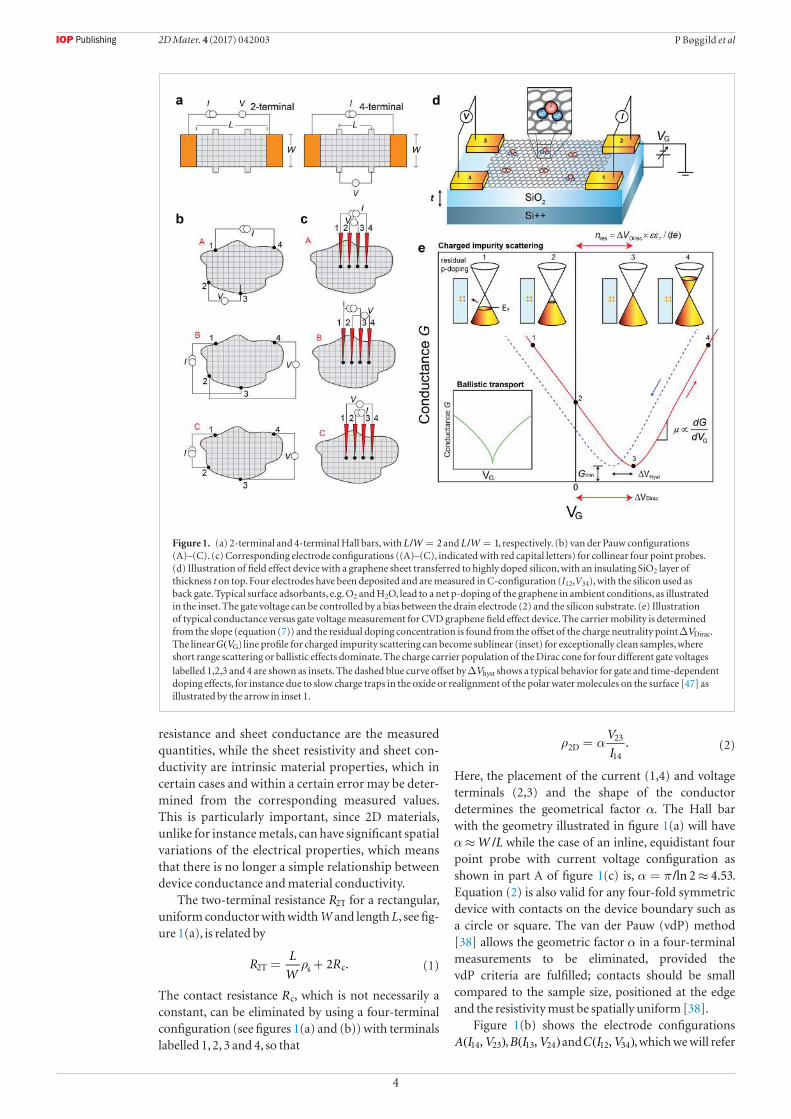
The two-terminal resistance R2T for a rectangular, uniform conductor with width W and length L, see fig-ure 1(a), is related by
ρ= +RL
WR2 .2T s c (1)
The contact resistance Rc, which is not necessarily a constant, can be eliminated by using a four-terminal configuration (see figures 1(a) and (b)) with terminals labelled 1, 2, 3 and 4, so that
ρ α=V
I.2D
23
14 (2)
Here, the placement of the current (1,4) and voltage terminals (2,3) and the shape of the conductor determines the geometrical factor α. The Hall bar with the geometry illustrated in figure 1(a) will have α≈W L/ while the case of an inline, equidistant four point probe with current voltage configuration as shown in part A of figure 1(c) is, α π= ≈ln 2 4.53/ . Equation (2) is also valid for any four-fold symmetric device with contacts on the device boundary such as a circle or square. The van der Pauw (vdP) method [38] allows the geometric factor α in a four-terminal measurements to be eliminated, provided the vdP criteria are fulfilled; contacts should be small compared to the sample size, positioned at the edge and the resistivity must be spatially uniform [38].
Figure 1(b) shows the electrode configurations A I V,14 23( ), B I V,13 24( ) and C I V,12 34( ), which we will refer
Figure 1. (a) 2-terminal and 4-terminal Hall bars, with / =L W 2 and / =L W 1, respectively. (b) van der Pauw configurations (A)–(C). (c) Corresponding electrode configurations ((A)–(C), indicated with red capital letters) for collinear four point probes. (d) Illustration of field effect device with a graphene sheet transferred to highly doped silicon, with an insulating SiO2 layer of thickness t on top. Four electrodes have been deposited and are measured in C-configuration (I12,V34), with the silicon used as back gate. Typical surface adsorbants, e.g. O2 and H2O, lead to a net p-doping of the graphene in ambient conditions, as illustrated in the inset. The gate voltage can be controlled by a bias between the drain electrode (2) and the silicon substrate. (e) Illustration of typical conductance versus gate voltage measurement for CVD graphene field effect device. The carrier mobility is determined from the slope (equation (7)) and the residual doping concentration is found from the offset of the charge neutrality point ∆VDirac. The linear ( )G VG line profile for charged impurity scattering can become sublinear (inset) for exceptionally clean samples, where short range scattering or ballistic effects dominate. The charge carrier population of the Dirac cone for four different gate voltages labelled 1,2,3 and 4 are shown as insets. The dashed blue curve offset by ∆Vhyst shows a typical behavior for gate and time-dependent doping effects, for instance due to slow charge traps in the oxide or realignment of the polar water molecules on the surface [47] as illustrated by the arrow in inset 1.
2D Mater. 4 (2017) 042003
5
P Bøggild et al
to throughout the article. The reciprocal configura-tions are ′A I V,23 14( ), ′B I V,24 13( ) and ′C I V,34 12( ).
The resistivity ρ for an arbitrarily shaped, uniform 2D conductor is then defined by
− =πγ ρ πγ ρ− −e e 1,R RA s B s/ / (3)
where RA and RB are the resistances measured in two different current–voltage configurations A and B. Here γ = 1 for contacts positioned at the edge and γ = 2 for inline, equidistant contacts far away from the edge [39].
For the van der Pauw geometry, the Hall resistance RH, Hall carrier density nH and Hall mobility µH can be determined by applying a magnetic field B normal to the sample surface.
µσ
=−
=
=
′R
R R
nB
qR
en
2,
, and
.
B BH
HH
Hs
H
(4)
For collinear four-point probe measurements on an infinite film, there is no Hall effect, only the Corbino effect due to current rotation.
2.3. DC conductivity of grapheneGraphene is a zero-gap semiconductor where the valence and conduction bands meet in 6 Dirac points, at the edge of the Brillouin zone. The six points belong to two sets labelled K′ and K, as a consequence of the graphene lattice consisting of two inequivalent triangular sub-lattices. The energy dispersion around the K and K′-points is linear within 1 eV of the Dirac points. Electrical current in graphene is carried by low energy, massless quasiparticles around the K and K′ points, termed Dirac fermions. The electronic structure and transport properties of graphene is covered extensively in literature, e.g. the excellent review articles by Castro Neto et al [40] and Das Sarma et al [41].
The sheet conductivity σs, sheet carrier den-sity n and sheet carrier mobility µ, are related by σ µ= nes . Semiclassical Boltzmann transport theory gives the simple relation [42]
σ =e
hk
2s
2
F mfp (5)
where π=k nF1 2( ) / is the Fermi wavenumber,
and τ= vmfp F is the elastic mean free path for a momentum relaxation time τ. Equation (5) can also be obtained by inserting the effective mass of the Dirac fermions [40, 41], =∗m k vF F/ , in the DC Drude conductivity, /σ τ= ∗ne ms
2 . The carrier mobility µ σ= ne/( ) can then be written as
µπτ=
e
h nv
2F (6)
where ≈ −v 10 m sF6 1 is the Fermi velocity. Here we
note that mfp represents the smallest scale at which
conductivity has any meaning; below this scale, the transport is ballistic and non-local.
The carrier mobility µ and residual carrier density n are usually determined by a field effect or a Hall effect measurement with a rectangular or quadratic sample geometry, see figure 1(d). In the field effect measure-ment, the carrier density =n CV eG/ is varied by a gate voltage VG. Here ε ε=C tr0 / is the capacitance per area of the capacitor formed by the graphene and the gate electrode, separated by a dielectric layer of thickness t and permit tivity εr. This approximation only holds if the linear dimensions of the overlap area between gate and graphene are significantly larger than the spacing t, so that the electric fringe fields can be ignored.
In addition to the plate capacitance, the low den-sity of states D of materials such as graphene leads to a contrib ution from the quantum capacitance =C e DQ
2 that can be neglected for typical silicon oxide dielectric layers with thickness in the 90–300 nm range, but can be significant for very thin gate layers [43]. Assuming electrical homogeneity, σ= =W L G Gs s( / ) , the field effect mobility µ can be estimated from the slope of the measured conductance as a function of gate voltage (see figure 1(e)),
µ≈∆∆C
L
W
G
V
1.
ox G (7)
The discussion of different methods for extracting carrier mobility is covered by numerous authors [44–46]. The residual carrier density, ε ε=ni r0 ∆ −V teDirac
1( ) , is determined from the gate voltage offset ∆Vdirac of the gate voltage corresponding to the minimum conductance, Gmin.
2.4. Scattering mechanisms and mobility of CVD grapheneGraphene grown by CVD is often transferred by wet transfer, with the copper either etched [10] or delaminated [18], using a polymer film as a mechanical support. The residual carrier density of the final device may be influenced by numerous factors, including doping by gas and water molecules adsorbed on the surface or trapped between the graphene and the substrate [47, 48], polymer residues from the transfer or lithographic processes [49], and surface treatments of the substrate (i.e. O2 plasma) [50]. Trapped charges in the oxide as well as water molecules and other polar molecules can lead to dynamic (hysteretic) variations in the total carrier density through capacitive gating or charge transfer [47].
Many of these factors also contribute to reducing the carrier mobility through different scattering mech-anisms. Most of the above external influences can be described by some form of charged impurity (ci) scattering.The scattering time for charged impurity scattering has a square-root dependence on the car-rier density, τ ∝ n nci s imp/ , where nimp is the density of charged impurities [51]. Comparison with equa-tion (6) gives the frequently observed linear relation between the conductance and the gate voltage in CVD
2D Mater. 4 (2017) 042003
6
P Bøggild et al
graphene, where the carrier mobility remains roughly constant, see equation (7). Tears, cracks, and grain boundaries produce point-like defects, which accord-ing to Chen et al [52] give rise to strong short-range scattering potentials, τ π= e h n n k R2 lnsr
2sr
2F( / )( / ) ( ),
which by insertion in equation (6) gives a nearly con-
stant mobility µ π= −n e h k R2 lnsr1 2
F( / ) ( ). Here R is the
radius of the point-like scattering potential, and nsr is the defect density.
Even in the absence of defects and contamination, electrons will scatter on intrinsic longitudinal acoustic phonons (LA), or, depending on the substrate, inter-act with substrate phonons (S) such as the polar opti-cal phonons in SiO2. This leads to a Matthiesens-rule expression for the total scattering time [53],
τ τ τ τ τ= + + + +− − − − − ...,tot1
ci1
LA1
S1
sr1 (8)
which is proportional to the carrier mobility, see equation (6).
After transfer to the target substrate, typical values for the carrier mobility are in the range of 500–5000
− −cm V s2 1 1 with residual doping levels of 1012–1013 cm−2. These values are far below the limit of approxi-mately 40 000 − −cm V s2 1 1 imposed by polar optical phonon scattering by the silicon dioxide [54], as well as the ca. 120 000 − −cm V s2 1 1, which represents the upper limit at room temperature, limited by longitudinal acoustic phonon scattering [41]. By careful optim-ization of growth and transfer, room temper ature mobilities of 5–12 000 cm2 V−1 s−1 were measured in high vacuum on Si/SiO2 [55]. Chen et al [56] found that for high quality graphene on a SiO2 substrate, charged impurity scattering is dominating.
With the increase of CVD grown graphene single crystals to cm-scale [57, 58] and general improvement of the large-area synthesized graphene films processes, one of the main limiting factors for graphene device quality is the transfer process. Encapsulation of gra-phene can greatly reduce the residual doping level and hysteresis, reduce the impurity and electron–phonon scattering, as well as provide stability towards changes in environmental conditions. While CVD graphene has been demonstrated to match the best exfoliated gra-phene devices produced by dry transfer (avoids water and solvents) with support [59] or by full encapsulation [20] in hexagonal boron nitride, a scalable route to high quality encapsulation is still highly desired. Hexagonal boron nitride encapsulation provides at the same time protection against doping by gas molecules and water molecules, polymer residues, lithographic damage, substrate phonons (compared to SiO2), and has been shown to reduce the roughness of graphene to extremely small values (12 pm) [60]. Followingly, it is imperative to develop large area encapsulation based either on high quality CVD processes for hexagonal boron nitride [61–63], or reasonable alternatives, including atomic layer deposition [64] or self-assembled monolayers [56, 65], or combinations of these. Without encapsu-lation, CVD graphene materials are not likely to reach
carrier mobilities better than 5000 − −cm V s2 1 1, and time will show how much improvement cost-effective, large-area encapsulation schemes can provide. For applica-tions such as electrodes, the sheet conductance can be increased via doping. CVD graphene can reach sheet resistances of order 100 Ω using surface doping with FeCl3 or Au doping of monolayers [66], or towards 20 Ω for FeCl3 intercalation in multilayer graphene [67].
2.5. AC conductivity for pristine and structured grapheneWhile the absorption of electromagnetic radiation in the visible spectrum is a constant 2.3% in single-layer graphene [68] and dominated by interband scattering, the photon energy is much smaller (meV) in the terahertz range, leading to predominance of intraband scattering of charge carriers, see figure 2. In this frequency range, the optical response of graphene is comparable to that of an electron plasma (or metal-like), while the optical conductivity of graphene is surprisingly well described by the same functional form as the classical Drude model [69]. The main assumptions behind the Drude model are that charge carriers are accelerated by an external field E, = −v eE me˙ / , that scattering events are instantaneous
and isotropic with an average scattering time τ, and that there is no interaction between charge carriers. Based on these assumptions, the Drude conductivity spectrum of a metal or a doped semiconductor is
σ ωσωτ
=−1 i
,dc( ) (9)where the DC conductivity is given by σ τ= ∗ne mdc
2 / and ω πν= 2 is the angular frequency. While Dirac fermions have zero rest mass, the quantum-mechanical treatment within Boltzmann transport theory of the electrodynamic response of graphene shows that the optical conductivity in the THz range has a Drude-like spectral shape [70, 71], with the DC conductivity given by the Boltzmann result, equation (5) [72].
THz time-domain spectroscopy measures the transmission amplitude and phase through a sample, which can be used to extract the spectral shape of the conductivity spectrum and thus allows the DC conduc-tivity and the scattering time to be extracted by fitting with equation (9). From these primary parameters, the carrier concentration and the drift mobility can then be calculated as will be discussed in section 5.7.
The Drude picture can be successfully extended to describe more complex scattering scenarios. In the simple Drude picture, the assumption of point-like, isotropic scatterers works well for high quality gra-phene on silicon dioxide substrates, where charged impurities tend to dominate, see section 2.4. The situa-tion can be quite different for graphene grown by more application-relevant processes, where polycrystalline copper foil is used, and the growth rate is accelerated to give the highest possible throughput. Such gra-phene films will tend to be polycrystalline in nature, with crystal domain sizes and orientations determined
2D Mater. 4 (2017) 042003
7
P Bøggild et al
by multiple factors, including purity, smoothness and orientation of the substrate, as well as the growth conditions. Additionally, defects during post-growth transfer to other substrates may introduce folds, buck-les, rips and tears in the film. These types of defects share the common feature that they are extended, or line-shaped, and results in scattering profiles that dif-fer qualitatively from isotropic.
Line-shaped defects generally lead to predomi-nance of backscattering. As the characteristic dimen-sions of the crystal domains in graphene approaches that of the mean free path mfp, the carriers will be subject to significant backscattering on the domain boundaries in addition to point-like impurity scatter-ing. As discussed by Smith [74], this increased prob-ability of backscattering of the charge carriers can be seen as a sign reversal of the current impulse response function (IRF), which in the Drude model is a simple exponential function, τ= −j t j t0 expd d( )/ ( ) ( / ). The Drude conductivity spectrum (equation (9)) is the Fourier transform of this IRF. With a modified IRF of the form τ τ= − −j t j ct t0 1 exp( )/ ( ) ( / ) ( / ), the corre-sponding conductivity spectrum is
( ) ⎜ ⎟⎛⎝
⎞⎠σ ω
ωτ ωτ=−
+−
W c
1 i1
1 i,DS
D (10)
a relation known as the Drude–Smith conductivity [74]. The parameter c describes the amount of backscattering (− c1 0⩽ ⩽ ). The Drude model is recovered for the case of no preferential backscattering, =c 0, and = −c 1 describes backscattering of every electron trajectory during one cycle of the AC-field. The DC conductivity then becomes +W c1D( ), where τ= ∗W ne mD
2 / (the Drude weight) can be understood as the local, intrinsic DC conductivity between the line defects.
For maximal backscattering, = −c 1, the DC conductivity is completely suppressed, as could be
expected for a macroscopic surface with charge car-riers strictly confined to small domains. There is no straightforward link between the backscattering parameter c and the microscopic structure of the con-ductive film, and as such, the model is phenomeno-logical by nature, in the same way as the original Drude model. However, under certain simplified condi-tions (identical, isotropic and spherical domains), the backscattering parameter can be linked to the charge reflection probability as α= − +c p 1 2r/( / ) where α is the ratio between the domain size and the mean free path mfp [75]. Hence, while equation (10) is a solid phenomenological basis for characterization of the conductivity of extended graphene films [26] as well as other nanostructured conductors [76] and semicon-ductors [77–80], the Drude–Smith model represents a highly simplistic picture of the complex interac-tion between Dirac fermions and line-defects, and its impact on the AC conductivity. Further investigations into the validity range of the Drude–Smith model as well as more specific models taking disorder explicitly into account are certainly needed for a detailed under-standing of conductivity dynamics in the presence of disorder in graphene.
2.6. Electrical uniformity and continuity of large area grapheneIt is clear that nearly any commercial applications of graphene that rely on the electrical properties cannot accept significant variability from sample to sample, nor within same sample. For instance, sheet resistivity variations in large area electrodes leads to inconsistent light emission of light emitting diodes [81].
As mentioned in section 2.3, the measured sheet conductance is strictly equal to the intrinsic sheet conductivity σs only in the case of perfect electrical uniformity. In the majority of published literature
Figure 2. (a) Optical conductivity of graphene from the THz to the visible frequency range. The absorption in the visible and near-infrared range is dominated by interband transitions with a constant value of 2.3% per graphene layer, while the low-frequency conductivity originates mainly from intraband transitions. (b) Illustration of intraband transitions for large and small negative Fermi energy, where interband transitions are suppressed for low frequencies (energies) and for large negative or positive Fermi energy. For high frequencies, interband transitions dominate over intraband transitions. The figure is modified from figure 1 in Sensale-Rodriguez et al [73], with permission from the author.
2D Mater. 4 (2017) 042003
8
P Bøggild et al
discussing methods for growth, transfer or passiva-tion/encapsulation for graphene, the uniformity is stated simply as a range of σs, ρ and n values measured across several devices, with an indication of statistical spread, or sometimes histograms [18, 55].
For large area graphene, the average and the sta-tistical spread itself are generally insufficient descrip-tors of uniformity. Growth and transfer processes can give rise to long-range spatial variations that need to be understood and monitored, and have non-trivial impact on the electrical characteristics. For instance, temperature or gas flow fluctuations or variations in a CVD reactor or the geometrical circumstances of a transfer procedure, can translate into spatially dependent variations in doping density as well as grain structure. In lieu of spatially resolved electrical measurements, optical microscopy and micro-Raman microscopy are used to assess and compare the uni-formity (see figure 6). While certainly relevant [82], it is doubtful that such indirect characterisation tech-niques can fully replace direct measurement of the conducting properties.
Conductivity variations can be decomposed into carrier density and carrier mobility variations [24, 27, 83],
σ µ=x y n x y e x y, , , .s( ) ( ) ( ) (11)
The vdP theorem, equation (3), requires the device to have no variations of (n,µ) within the boundaries of the sample. A crack or a tear crossing the boundary of the sample will not violate the basic assumptions; in this case the sample can be regarded as simply having a different, more irregular shape. In contrast, an internal tear or hole will indeed lead to errors in the estimation of σs [84].
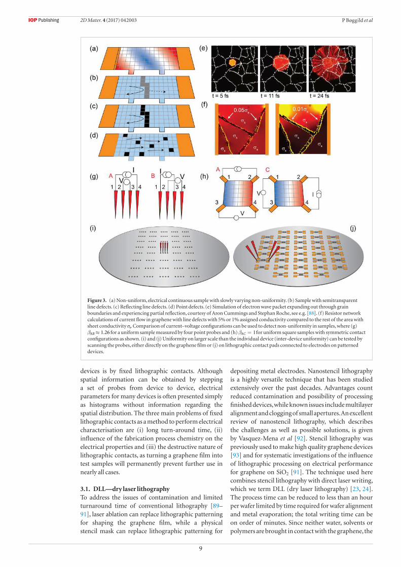
The electrically measured sheet conductance (sheet resistance) is strictly different from the conductivity (resistivity) of a graphene film, and these differences can lead to non-trivial errors when changing the carrier density with an electrostatic gate. Due to the ambipolar behavior of graphene, spatial variations in n or µ on the same scale as the sample size will lead to inhomogene-ous current flow as a function of gate voltage, as differ-ent regions of the graphene sample become more or less conducting at different gate voltages, see figure 3(a). In this case, the effective shape of the sample is gate-voltage dependent, making determination of carrier mobility or density from the gate-voltage dependent conduct-ance prone to systematic errors, as we showed recently in [85]. Following our previous work [26] we refer to this aspect of uniformity as electrical continuity.
Figures 3(a)–(d) shows four different scenarios. In figure 3(a) the conductivity is non-uniform with a slow variation, but no disruption of the current flow. In figures 3(b) and (c) a line defect is crossing the cur rent path. If the line is semitransparent, as for instance most grain boundaries, current can still be transmitted across the defect (b), while for a tear or crack, the cur rent may be disrupted entirely. Figure 3(e) shows a simulation of an electron wave packet spreading out from a point
cur rent source in polycrystalline graphene, while expe-riencing partial reflections at the grain boundaries, in analogy to the illustration in figure 3(b). Figure 3(f) shows calculations of current flow in a graphene sam-ple using a resistor network model, where each resis-tor represents an area of graphene with a local carrier density and carrier mobility, and conductivity given by σ µ= nes . The lines represent areas where the conduc-tivity of the resistors have been reduced to 5% and 1% compared to the rest of the structure, resulting in a dra-matic difference in how the current flow is redirected.
The spatial distribution of any number of insulat-ing defects can have a large impact on current trans-port. In one cm2 of graphene, one missing line of atoms across the film, while just amounting to 1 out of 80 million atoms, will prevent current flow, except for possibly quantum tunneling across the 1 atom wide gap. On the other hand, when distributed uniformly, figure 3(d), the exact same amount of defects will have virtually no influence on the transport properties, as the resulting 1 vacancy per 1.5 µm2 per graphene is orders of magnitude lower than the point defect lev-els studied by Cancado et al [86]. This trivially reflects that line defects and point defects have very different impact on the measured KPIs, and that the average defect density itself is an unreliable predictor of the electrical performance unless the defect distribution is also considered.
For lithographically patterned graphene films, it is relevant to distinguish between uniformity and conti-nuity on inter-chip and intra-chip level. On the inter-chip level, the statistical and spatial variations of the conductance, carrier density and mobility can be com-pared across the wafer. The intra-chip uniformity can be assessed by the van der Pauw method, by compar-ing electrical measurement of the resistance in differ-ent current voltage configurations with the theoretical result from a perfectly uniform sample. We introduce the uniformity parameter, β = R Rij i j/ , where i and j represent two different current–voltage configurations. For a four-point probe measurement far from the edges, figure 3(g), β = 1.26AB , while for the case of a symmet-ric van der Pauw square-shaped sample, figure 3(h), β = 1AC . In both cases, a closer inspection of this ratio can reveal information on the type of non-uniformity, i.e. whether the origin is point- or line-defects [25, 26, 87], and whether the observed variations are dominated by doping or mobility variations [85].
Finally, the scale at which non-uniformity occurs is important; 500 nm graphene domains with high resis-tive grain boundaries, may lead to strongly irregular current paths for submicron devices, but can appear homogeneous on mm-scale where many statistically similar domains are averaged.
3. Mapping with fixed contacts
The most common form of providing information on the electrical properties of large-area graphene
2D Mater. 4 (2017) 042003
9
P Bøggild et al
devices is by fixed lithographic contacts. Although spatial information can be obtained by stepping a set of probes from device to device, electrical parameters for many devices is often presented simply as histograms without information regarding the spatial distribution. The three main problems of fixed lithographic contacts as a method to perform electrical characterisation are (i) long turn-around time, (ii) influence of the fabrication process chemistry on the electrical properties and (iii) the destructive nature of lithographic contacts, as turning a graphene film into test samples will permanently prevent further use in nearly all cases.
3.1. DLL—dry laser lithographyTo address the issues of contamination and limited turnaround time of conventional lithography [89–91], laser ablation can replace lithographic patterning for shaping the graphene film, while a physical stencil mask can replace lithographic patterning for
depositing metal electrodes. Nanostencil lithography is a highly versatile technique that has been studied extensively over the past decades. Advantages count reduced contamination and possibility of processing finished devices, while known issues include multilayer alignment and clogging of small apertures. An excellent review of nanostencil lithography, which describes the challenges as well as possible solutions, is given by Vasquez-Mena et al [92]. Stencil lithography was previously used to make high quality graphene devices [93] and for systematic investigations of the influence of lithographic processing on electrical performance for graphene on SiO2 [91]. The technique used here combines stencil lithography with direct laser writing, which we term DLL (dry laser lithography) [23, 24]. The process time can be reduced to less than an hour per wafer limited by time required for wafer alignment and metal evaporation; the total writing time can be on order of minutes. Since neither water, solvents or polymers are brought in contact with the graphene, the
Figure 3. (a) Non-uniform, electrical continuous sample with slowly varying non-uniformity. (b) Sample with semitransparent line defects. (c) Reflecting line defects. (d) Point defects. (e) Simulation of electron wave packet expanding out through grain boundaries and experiencing partial reflection, courtesy of Aron Cummings and Stephan Roche, see e.g. [88]. (f) Resistor network calculations of current flow in graphene with line defects with 5% or 1% assigned conductivity compared to the rest of the area with sheet conductivity σs. Comparison of current–voltage configurations can be used to detect non-uniformity in samples, where (g) β ≈ 1.26AB for a uniform sample measured by four point probes and (h) β = 1AC for uniform square samples with symmetric contact configurations as shown. (i) and (j) Uniformity on larger scale than the individual device (inter-device uniformity) can be tested by scanning the probes, either directly on the graphene film or (j) on lithographic contact pads connected to electrodes on patterned devices.
2D Mater. 4 (2017) 042003
10
P Bøggild et al
film is as pristine as the handling and transfer process allow. Apart from serving as a fast prototyping and test method, it also provides a reference for comparison with non-contact methods [24], see section 6.
To pattern the graphene as well as for machining the physical shadow mask, a Micromac AG microSTRUCT vario laser micro-machining system was used. First, an array of large Au electrodes was deposited through a physical shadow mask. To establish the optimal laser fluence parameters for three different wavelengths (355 nm, 532 nm and 1064 nm) the single 10 ps pulse fluence was increased from about 1 to 300 mJ cm−2 until the onset of graphene ablation was detected, by noting when the electrical resistance between the electrodes increased towards infinity. A range of laser fluence values could be established for all three wave-lengths, where the graphene is fully removed without damaging the SiO2 surface. This was confirmed by optical microscopy, micro-Raman spectr oscopy, stylus profilometry and electrical measurements, as summa-rized in figure 4. By optimizing the fluence and the pat-tern layout to only consist of line cuts, the writing time could be reduced to less than 1 s per device.
3.2. Uniformity analysisThe uniformity and quality of lithographically defined samples can be analysed in some detail following the strategies outlined in section 2.6, using the uniformity
parameter β = R RAC A C/ for the two measurement configurations A and C in figure 3(h). A set of 47 working (5 mm × 5 mm) samples was fabricated by DLL and measured in both configurations to establish the conductance, the field effect mobility, and the Hall mobility in a transverse magnetic field. Uniformity and continuity was assessed from the deviation of the βAC ratio from unity. Out of the 47 samples, 20 samples had βAC value between 0.9 and 1.1, indicating high uniformity. For these devices, typical figure-of-merit values at zero gate bias voltage were a sheet conductance of 3 mS, Hall mobility of 800–1000 cm2 V−1 s−1 and a zero-gate bias carrier density of approximately −10 cm13 2, representing a fairly high residual doping level. These results are directly compared to THz-TDS measurements in section 6.1.3.
Figure 5(a) shows how the variation of βAC is an indicator of the effective sample aspect ratio, in this case from 1 (square) towards rectangular. In figure 5(b) the deviation of the uniformity parameter βAC from unity is illustrated schematically for a geometrical, gate-inde-pendent contribution, β GAC( ), and/or a gate-dependent contribution, β∆ AC. While β GAC( ) originates from tears, cracks and holes (disruptions), which change the effective geometry of the sample, non-uniformity in carrier mobility and carrier density, however, will lead to gate-dependent variations. In figures 5(c) and (d) the sheet resistance Rs and uniformity βAC of a graphene
Figure 4. DLL lithography for fast prototyping of wafer scale 2D materials. (a) After transfer of CVD graphene to the substrate, (b) contact metal is deposited through a shadow mask. (c) The graphene device and lead areas are then cut out by laser ablation and (d) the devices are finished. (e) 4″ wafer with 49 devices. (f) Device layout with numbers 1–4 indicating electrodes used in this study. (g)–(j) optical and (k)–(n) micro-Raman microscope images of graphene 2D-peak intensity after irradiation of a vertical line with laser fluence from 30 to 241 mJ cm−2. In the laser fluence range between 50 and 200 mJ cm−2 the graphene is entirely removed while the SiO2 is not damaged. Adapted from [23].
2D Mater. 4 (2017) 042003
11
P Bøggild et al
device measured in dry N2 atmosphere conditions is shown. In comparison, an exfoliated graphene device fully encapsulated in hexagonal boron nitride using methods described in [94], shows far smaller uniform-ity variation β∆ AC, see figures 5(e) and (f). Figure 5(g) shows a result of a finite element simulation for a sam-ple, using the carrier density estimated from the Raman G-peak linewidth [95] to estimate the carrier density, see figure 5((g), inset). The simulated (dashed) curves agree reasonably well with the experimental (full) curves. Fig-ure 5(h) show the result of Monte Carlo simulations of 40 devices with random distributions of carrier density. There is a clear relation between the degree of non-uni-formity β∆ AC caused by doping variations and the error in estimation of the average carrier mobility. Also, using the van der Pauw equation is shown to greatly reduce the mobility measurement error. Alas, we conclude that four-terminal measurements are not reliable indicators for graphene carrier mobility, unless the graphene is very homogeneous or the dual configuration (van der Pauw) approach is used.
4. Mapping with movable contacts
Despite the mechanical strength of graphene, its atomic thinness makes the films very fragile, and susceptible to damage upon physical contact. Conventional
millimeter-size spring-loaded tungsten tips used for mapping of sheet resistivity of silicon wafers, are difficult to use on graphene films without causing unreliable measurements, if not irreversible damage.
4.1. Micro-four point probes (M4PP)The micro four-point probe (M4PP) was introduced in 2000 as an ultra-compact, non-invasive alternative to conventional automated four-point probe systems, suitable for characterisation of thin films and fragile surfaces, with a far better spatial resolution, increased surface sensitivity, as well as reduced damage and contamination [96]. The M4PP is a silicon chip with multiple (typically 4 or 12) micro-fabricated metal-coated cantilever electrodes. Multiplexing of the current and voltage probes allows for multiple current–voltage configurations to be measured in a single engage. This allows a system to detect measurement inconsistencies, which can be caused by non-uniformity of the samples, and can also provide insight into the scale of spatial variations, as was done for characterization of laser annealed ultra-shallow junctions [97]. The M4PP has been used for a large variety of low dimensional systems, including surface reconstructions in ultra-high vacuum (UHV) [98], self-assembled polymer films [99], carbon nanotubes [100], metal nanowires [101] as well as industrially relevant systems such as magnetic
Figure 5. Uniformity analysis from field effect measurements. (a) The uniformity parameter /β = R RAC A C is plotted against aspect ratio of a rectangular sample, showing that the gate independent part of βAC is a very sensitive indicator of the effective sample geometry. (b) βAC as a function of gate voltage can exhibit a constant offset for static geometrical variations (i.e. only disruptions, such as cracks and tears), or gate dependent variations β∆ AC since the effective shape of the sample changes as a function of gate bias for non-uniformly doped graphene (or non-uniform mobility). (c) Sheet resistance /π=R R ln 2As (blue) and /π=R R ln 2Cs (red) compared to RvdP (black) derived resistivity for non-passivated CVD graphene. (d) Uniformity parameter βAC for same sample. (e) Rs and (f) βAC plotted for exfoliated graphene sample fully encapsulated in hexagonal boron nitride. Both the geometrical and doping uniformity is significantly higher for the encapsulated sample. (g) The residual doping level derived from the Raman spectrum (linewidth of G-peak) of a CVD sample is used as input for finite element calculation, allowing simultaneous fitting of the RA, RC and Rs data. (h) Monte Carlo calculation of estimation error for carrier mobility as a function of β∆ AC for 40 devices, with random, spatial carrier density variations. Adapted from [85].
2D Mater. 4 (2017) 042003
12
P Bøggild et al
tunnel junctions and ultra-shallow junctions [83]. Compared to the classic theory of four-point probe measurements [102], substantial progress have been made with respect to error-correction and sensitivity analysis, as well as new measurement concepts such as the micro Hall method [103] which is also applicable to graphene. M4PP today ranks with fixed lithographic electrodes in terms of precision and repeatability for both sheet resistance and Hall effect measurements
[104], while being non-invasive and superior in terms of throughput. Automated M4PP mapping was first introduced for mm-size self-assembled poly-thiophene monolayer [99] and later used for mapping of the carrier density and mobility of graphene [24–27]. Alternative approaches to conductivity mapping include multi-tip scanning probe systems [105–108], which have less relevance for large area graphene due to a low throughput.
Figure 6. (a) SEM image of micro 12-point probe. (b) M4PP with four cantilevers and strain sensor for contact detection. (c) Optical image of a 6 × 8 mm graphene film grown on polycrystalline Cu foil (sample ‘Cu foil 1’) where the transfer process was imperfect, and several damaged areas are clearly visible. (d) The Raman spectrum intensity peak ratio ( ( )/ ( ))−I ID G 1 map shows much less features than the (e) I(G) map, which suggests that the macroscopic damage (tears, gaps, holes, cracks) dominate over structural (atomic scale) defects. (f) The conductivity map is very similar to the I(G) peak map. (g) Resistance ratio /β = R RAB A B map. (h) Histogram of βAB values for sample ‘Cu foil 1’ (red bars) and sample ‘Cu111’ (green bars), where the ‘Cu111’ (CVD graphene on single crystal Cu catalyst) is showing a far better agreement with the prediction for continuous graphene. Adapted from Buron et al [25].
2D Mater. 4 (2017) 042003
13
P Bøggild et al
4.2. Conductance mapping with M4PPCommercial tools for fully automated M4PP mapping of 100 mm to 300 mm wafers with automated wafer as well as probe changing (in case of wear or failure), have been developed and are routinely used in the semiconductor industry6. To allow for fully automated measurements on CVD graphene without 100% coverage mechanical surface detection is achieved by on-chip integrated strain gauge sensors [83].
Figure 6(a) shows a 12-point probe useful for measurements at different length scales.
Figure 6(b) shows a M4PP with a strain sensor for contact detection, hovering above a graphene flake.
Figure 6(c) is an optical micrograph of a CVD grown graphene sample (‘Cu-foil 1’) where the trans-fer to the SiO2 substrate was imperfect, leaving sev-eral cracks and holes in the structure. Even within the areas with clear macroscopic damage as revealed in the Raman G-peak intensity map (figure 6(e)) the
−I ID G 1( ( )/ ( )) ratio shows only minor variations, underlining that the I ID G( )/ ( ) ratio alone is insuffi-cient to evaluate the impact of defects on the electrical continuity of the graphene film.
Figure 6(f) shows a conductance map with 4000 measurement points, recorded with a 10 µm pitch M4PP and a step size of 100 µm. There is a high resem-
blance of the G-peak intensity map and the M4PP conductance map, showing that the coverage of gra-phene is the main source of the conductance map vari-ations. Figure 6(g) shows a color map of the uniform-ity parameter βAB, which is described in the following section.
4.3. Uniformity analysis with M4PPThe histogram (figure 6(h), red bars) of the uAB ratio corresponding to the data in figure 6(f), shows a clear deviation from 1.26 for homogeneous graphene [25], even taking into account statistical spread from variations in probe distance, as calculated by Monte Carlo simulations (black curve). In comparison, the βAB data from sample ‘Cu111’, single-crystal Cu transferred by non-destructive electrochemical transfer [18], is in much better agreement with the expected distribution for undamaged graphene.
Any inhomogeneity in the vicinity of the four point probe may change the current flow, which in turn leads to deviations in the measured voltages, as discussed in section 2.6. Lotz et al [87] studied the deviations of the βAB ratio from the nominal value of 1.26 for a homogenous 2D film, in the presence of line defects using Monte Carlo based finite element calcul-ations. The study showed that a moderate number of line defects introduces a significant spread of βAB ratio values, and that strong line disorder leads to a collapse of βAB towards unity, where the cur rent flow between the current probes favors a single quasi-1D pathway,
Figure 7. Monte Carlo simulations of how near-insulating line defects influence the current flow in four point measurements. (a) Open line defects (cracks) with length equal to the probe spacing s, and with an average of 2.25 or 0.09 defects per area s2. (b) Distribution of βAB values for different open line defect densities, showing the transition from 2D current flow (β = 1.26AB ) for sparse defect landscapes to 1D current flow ( )β ≈ 1AB for dense line defects. Adapted from Lotz et al [87]. (c) Closed line defects (grains) with a high (4.00 s−2) and low (0.01 s−2) density. (d) Distribution of βAB values for closed defects (grains), showing similar transition from 2D to 1D current flow, but also recovery towards 2D-like flow (poly-2D, ⩽β 1.26AB ) as the grain boundary size becomes much smaller than s so that the film appears uniform on the scale of the probe (indicated by a white arrow). Adapted from Lotz et al [109].
6 The company CAPRES A/S, a spinout of the Technical University of Denmark, manufactures fully automated system based on micro four point probes (www.capres.com).
regardless of the current–voltage configuration. Typi-cal current flow patterns in 2D conductors with repre-sentative arrangements of line defects from the Monte Carlo ensemble are shown in figure 7(a), for 0.09 and 4.00 defects per area measured in units of square probe spacing, s2. As the density of line defects is increased, the distribution of βAB values shift from being cen-tered around 1.26 to being collapsed onto 1.00 onto 1.00. Compariso n with the statistical distribution of βAB values in figure 6(h) shows a striking resemblance, which corroborates the interpretation that the elec-tron transport in the incompletely transferred CVD graphene film, undergoes a transition from 2D-like (uninhibited) to 1D-like (percolative) current flow in the most damaged parts of the graphene sample. In the latter case, the current path is nearly unaf-fected by the change between cur rent terminals corre-sponding to A and B configurations, which results in β = 1AB . Figure 7(c) shows the corresponding case of closed, semitransparent line defects, which can be used to model grain boundaries in graphene. The transition from low defect density where the current flow is an approximating uninhibited 2D current flow, to a col-lapse towards 1D-like current flow for higher defect density, resembles the situation for open line defects. However, when the grain size becomes so small that the material appears uniform on the scale of the probe spacing, the βAB distribution is recovering towards the 2D value, β = 1.26AB , as indicated by the white arrow in figure 7(d) for 9 grains per s2.
Comparing the statistical distributions in fig-ures 7(b) and (d), it is not clear whether the open defects or closed defects model describes the data best; the data is equally well described by a mix of the types of behavior shown in figure 7.
5. Mapping without physical contact
In terms of mapping the electrical properties of graphene with a reasonable compromise between speed and accuracy, terahertz time-domain spectroscopy is the most well-studied in scientific literature, in addition to which commercial solutions for large-scale conductivity mapping of CVD graphene already exist7. For general overview of the terahertz properties of graphene, we recommend [71, 110]. In this section, the main focus is to overview the relevant terahertz based methodologies and results in terms of mapping the electrical KPIs of large-scale graphene films. However, several other complementary non-contact electrical characterisation and mapping techniques are under development. We will briefly overview these in the context of electrical KPIs, before focusing on terahertz-based methods.
5.1. Emerging non-contact techniques5.1.1. Terahertz based techniquesTerahertz time-domain spectroscopic measurement of electrical conductivity can be carried out by measuring the attenuation of a terahertz pulse by transmission through the sample (transmission-mode) or by reflection back (reflection-mode) from the sample. As discussed in much more detail in section 5.2, this attenuation can be translated to sheet conductivity. Conductivity maps are then formed by scanning the wafer with respect to the THz transmitter and receiver. Conceptual schematics of transmission and
Figure 8. Non-contact conductivity mapping conceptual schematic with corresponding examples of conductivity maps of graphene (on polymeric substrates). (a) Transmission based THz-TDS image of a ×20 20 cm conductivity map of graphene-on-PET. (b) Reflection based THz-TDS image of ×1 1 cm graphene sandwiched between two PE sheets. (Courtesy of Dr Albert Redo-Sanchez, Das-Nano). (c) Eddy current conductivity map of ×20 20 cm graphene-on-PET sheet (Courtesy of Dr Marcus Klein, Suragus sensors and Instruments). (d) Microwave impedance spectroscopy conductivity map of an ×18 18 cm graphene-on-PET.
7 The company Das Nano manufactures the systems for graphene conductivity mapping, based on reflection-mode THz-TDS spectroscopy. Source: www.das-nano.com
reflection mode THz-TDS are shown in figures 8(a) and (b), alongside examples of conductivity maps of CVD graphene on Polyethylene terephtalate (PET) and sandwiched between polyethylene (PE) layers, respectively. The conductivity map in figure 8(a) is recorded with the setup described in section 5.2, and illustrated in figure 9(b). The horizontal stripes are only visible in the conductivity map and originates from mechanical damage caused by the packaging box used to store the PET/CVD film. The conductivity map in figure 8(b) is recorded with a Das Nano Onyx reflection-mode THz-TDS mapping system. Reflection-based THz-TDS is less well-established and more complex than transmission-based THz-TDS, but has the advantage that the much wider range of terahertz absorbing (conducting) substrates can be used, as recently demonstrated [28].
5.1.2. Eddy currentAnother promising approach is eddy current (EC) measurements, where an induction coil is scanned across a thin film, while generating an oscillating magnetic field. This leads to eddy currents in the conductor, and the absorbed power can be converted into a DC voltage, which in turn is used to estimate the conductivity of the conductor [111–113].
While there have so far not been any examples in scientific literature of EC-based maps of graphene conductivity or other electrical properties [117], EC-based conductivity mapping methods and systems have long been known in the semiconductor and thin film industry [114]. Commercial manufacturer Sura-gus produces EC-based conductivity mapping systems that have been successfully demonstrated with wafer-scale graphene samples8 that can map sheet resistance
Figure 9. Illustration of different THz-TDS setups. (a) Illustration of custom-built free-space laboratory system used for ultra-broadband measurements up to 15 THz. (b) Setup with a commercial fiber optics spectrometer and photoconductive antennae for converting femtosecond laser pulses to terahertz pulses, and for readout of the terahertz signal after transmission through the target substrate. (c) Photo of setup during the mapping of the THz transmission of a 2″ silicon wafer. (d) Terahertz conductivity map and corresponding optical microscopy image of transferred graphene film on a terahertz transparent (high resistivity) silicon wafer.
2D Mater. 4 (2017) 042003
16
P Bøggild et al
with accuracy below 5% in a wide resistivity range, with a throughput corresponding to scanning of a 12″ wafer in 30 min at a pitch of 1 mm. Figure 8(c) illus-trates the eddy current technique, with a conductiv-ity map (40 000 measurement points) recorded by a Suragus EddyCus TF map 2525. In this setup, the sec-ondary magnetic field generated by the eddy current is measured by a pickup-coil. By reducing the size of the sensors and thus the distance to the surface, the resolu-tion can be reduced to the submicron scale [115], so this technique appears to offer a wide range of possi-bilities for adapting to different application scenarios. Similar to the micro four-point probe, the method allows information on the large-scale homogeneity of the sample to be extracted as well, since disruptions such as cracks, force the eddy currents to pass around the obstacle, which can be detected as a shift of imped-ance [113].
5.1.3. Microwave impedanceThe surface impedance and sheet resistance of graphene films on different substrates can be evaluated by induced shifts of the frequency and quality factor of a suitable electromagnetic cavity resonance, either by placing the sample inside the cavity at a field maximum [112, 116, 117] or in the evanescent near-field zone of an opening in the cavity [118], allowing spatial resolution in the nanometer range [119]. A more advanced version of the microwave resonator system was able to measure the average conductance of large areas nearly instantly, however without any spatial information [118, 120]. By localizing the probe area using a copper housing with a small opening and a sapphire microwave resonator inside, large-scale conductivity microwave impedance maps of graphene were obtained, see figure 8(d). In this scan, the time per measurement was 100 ms, and the reproducibility was found to be of order 1%, with uncertainties due to substrate thickness variations and permittivity below 10%. The resolution is given by the size of the resonator, which at present is between 5 to 20 mm, and for which pitch ranges between 3 to 15 mm are relevant, respectively. Microwave impedance-based conductivity mapping have a strong potential for fast, non-contact imaging of the electrical properties of graphene and other 2D materials.
5.1.4. Micro-Raman spectroscopyRaman spectroscopy is a widespread and well-established method for obtaining quantitative information about defects, disorder, strain, doping, number of layers in graphene sheets [30], all of which are known to affect the electrical properties. Graphene has two main characteristic peaks, which for a 532 nm laser are visible at approximately 2675 cm−1 (2D peak) and 1580 cm−1 (G peak).
The occurrence of a third peak (D-peak at 1350 cm−1) in the Raman spectrum indicates the presence of sp3 bonds, and is typically associated with structural defects in the basal plane of graphene, including edges with armchair orientation. Disorder can be quantified through the I(D)/I(G) peak intensity ratio, which is related to the average distance between defects [121, 122]. For low to moderate disorder levels, a higher I(D)/I(G) ratio means higher disorder in the system, which has been shown to correlate with lower carrier mobility in certain graphene systems [30].
The full width at half maximum (FWHM) of the graphene 2D-peak (Γ2D) can be used as an indicator of strain variations in graphene, which is linked to the mobility of graphene for high-quality devices, such as epitaxial graphene on SiC [123] as well as exfoliated graphene on SiO2 and on hexagonal boron nitride [31, 82, 91, 124]. A decrease in Γ2D correlates with an increase in mobility due to less lattice deformation, which also seems to hold for CVD graphene grown on Cu substrates [20]. Accordingly, the I(2D)/I(G) peak intensity is suggested to be a indicator of carrier mobil-ity limited by charged impurity scattering [125]. For larger doping levels > × −2 10 cm12 2( ) the peak posi-tions of the 2D- and G-peaks are more sensitive to doping, and can give information on doping levels and doping polarity (n or p) of graphene, while for smaller doping levels, the ΓG or the I(2D)/I(G) intensity peak ratio are better predictors of doping [95, 126].
Overall, Raman spectroscopy is invaluable for obtaining information essential for understanding and interpreting the electronic properties of graphene films and devices. The Raman spectrum is clearly affected by the carrier doping and mobility, however, but are not translated to electrical KPIs in any straight-forwards manner. Due to the widespread availability of high quality micro-Raman spectroscopy equip-ment in the graphene research field, further progress in establishing traceable links between quantitative micro-Raman microscopy and the electrical KPI’s of graphene will be of great importance.
5.2. Transmission-mode terahertz time-domain spectroscopyTHz-TDS is a method for determination of the complex-valued dielectric response of a material in the THz frequency range. We consider here exclusively THz-TDS based on transmission of terahertz pulses through the sample, as depicted schematically in figure 8(a).
The technique relies on femtosecond laser-based generation and synchronized, time-resolved detec-tion of the electric field E t( ) of an ultrashort electro-magnetic pulse with spectral components covering part of the THz spectral range [127]. Custom-built laboratory THz-TDS systems based on two-color fem-tosecond laser-induced plasmas [128–132] deliver spectroscopic results well into the multi-ten THz range [78, 133–138], see figure 9(a).
8 Suragus Sensors and Instruments manufactures eddy-current based machines for conductivity mapping of bulk and thin film materials. www.suragus.com.
With precise detection of the temporal waveform, a THz-TDS system gives access to the amplitude and phase of the signal within its useful bandwidth. Fig-ure 9(b) illustrates a much cheaper and simpler, typi-cal commercial spectrometer (from Picometrix, Inc.) based on photoconductive antennas which is capable of generation and detection in the range 0.1–4.0 THz. Figure 9(c) shows the system during scanning of a gra-phene coated silicon wafer, resulting in a map of the conductivity as shown in figure 9(d), together with a coverage map calculated from automated gigapixel optical microscopy [18, 139].
THz-TDS analysis is based on measurements of two time-domain signals, a reference signal recorded under well-known conditions, and a sample signal recorded after interaction with the sample material. The relevant parts of the signals are isolated by temporal windowing and Fourier transformed, giving access to the amplitude and phase of the signals at each frequency point ν within the spectral bandwidth. For conductivity characteriza-tion and mapping of graphene, measurements can be performed either in reflection or transmission configu-ration, with similar principles behind the spectroscopic analysis. For brevity, we will describe the transmission configuration here, but state the relevant analytical results for reflection geometry as well.
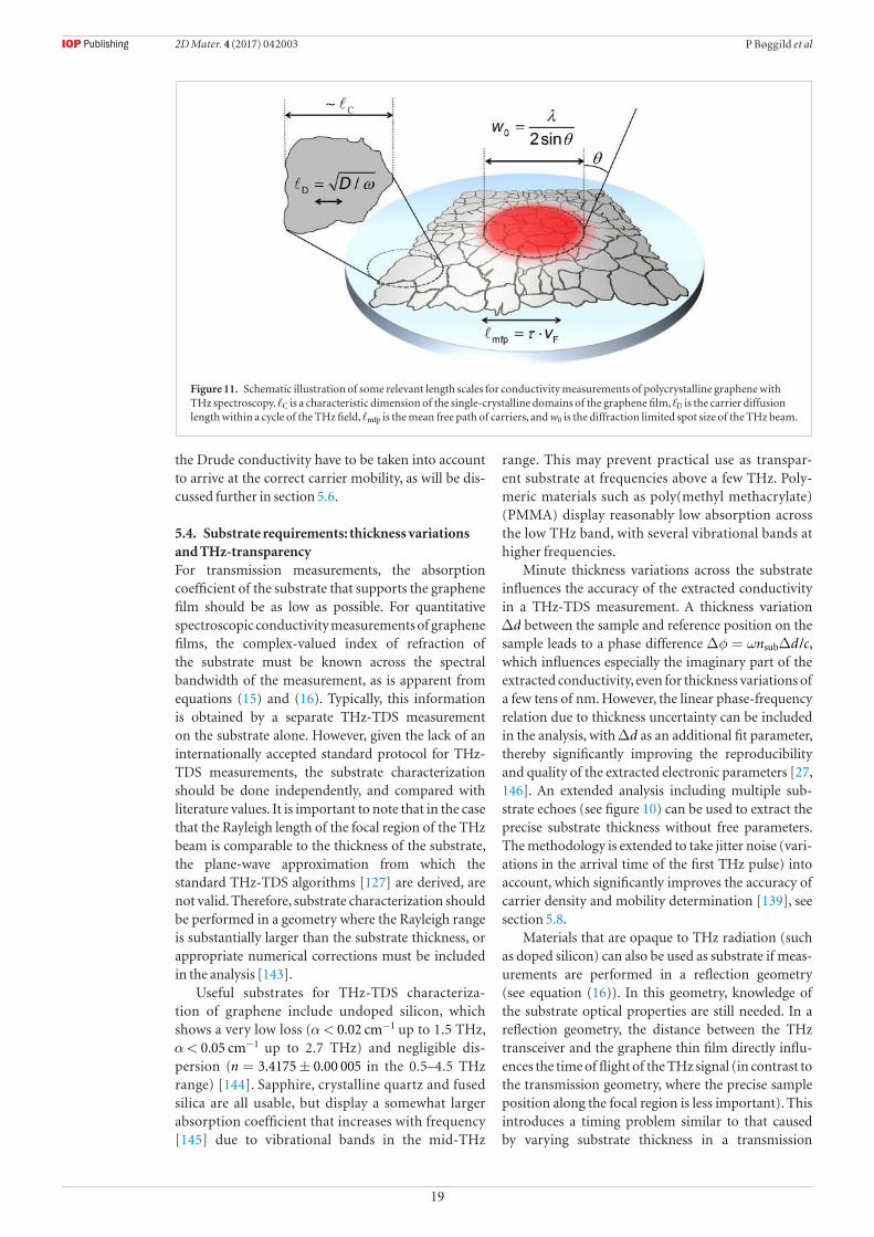
We consider the situation where the graphene layer is covering a part of the dielectric substrate, as illus-trated in figure 10 (inset), a scenario which was first described by Tomaino et al [140]. The THz beam is typ-ically focused to a diffraction-limited spot size, and the sample can be positioned so that the beam either passes through an uncovered section of the substrate (the ref-erence signal), or a section covered by graphene (the sample signal). In the frequency domain (ω πν= 2 ) and in the plane-wave approximation, the electric fields of the transmitted reference and sample signals are then
( ) ( ) ( ) ( )
( )
( ) ( ) ( ) ( )
( )
( )
( )
⎛
⎝⎜
⎞
⎠⎟
⎛
⎝⎜
⎞
⎠⎟
∑ ∑
∑ ∑
ω ω ω
ω
ω ω ω
ω
= = +
=−
= = +
=−
δ δ
δ
δ
δ δ
δ
δ
=
∞
=
∞
=
∞
=
∞
E E E t t r r
Et t
r r
E E E t t r r
Et t
r r
e 1 e
e
1 e,
e 1 e
e
1 e,
k
k
k
k
k
k
k
k
R0
ref 0 12i
231
23 21i2
012 23
i
23 21i2
S0
sam 0 filmi
231
23 filmi2
0film 23
i
film 21i2
(12)
where t t r r t r, , , , ,12 23 21 23 film film are the Fresnel transmission and reflection coefficients in and out of the uncovered and graphene-covered part of the substrate, respectively, and δ ω= n d csub / is the propagation phase through the substrate of thickness d and refractive index nsub. The infinite sums describe the multiple internal reflections of the short THz probe pulse in the substrate, as illustrated in figure 10. Here, a THz transient is recorded after transmission through a base substrate (black curve) and a single-layer graphene film on the same substrate (red curve).
The direct pass ER,S(0) as well as three subsequent echoes
ER,S(1-3) from the substrate are indicated.
As seen in the figure 10, the characteristic absorp-tion in the graphene film reduces the peak ampl-itude of the directly transmitted THz field by 15% compared to the reference, which is considerably more than the 2.3% absorption in the visible spec-trum [68], see figure 2. The first echo is subject to a larger reduction (47%) of the peak amplitude due to the two interactions with the graphene film (transmission and then reflection). This illustrates that depending on the strength of the interaction between graphene and the THz field, it can be advan-tageous to use the spectroscopic information con-tained in the echo signals, as well as in the directly transmitted signal.
Figure 10. THz-TDS data recorded on single-layer graphene on a silicon substrate. The inset shows the origin of the directly transmitted signal and the subsequent echoes from multiple passes in the substrate [25, 140].
2D Mater. 4 (2017) 042003
18
P Bøggild et al
In the thin-film limit, ( λ πd n2/( )), which almost by definition is perfectly fulfilled for graphene layers, the transmission- and reflection coefficients of the conductive film are
ωσ ω
ωσ ω
ωσ ωσ ω
ωσ ωσ ω
=+ +
=+ +
=− −+ +
=− −+ +
tn Z
tn
n Z
rn Z
n Z
rn Z
n Z
2
1, (from air side)
2
1, (from substrate side)
1
1, (from air side)
1
1, (from substrate side)
sub
film,airsub 0 s
film,subsub 0 s
film,airsub 0 s
sub 0 s
film,subsub 0 s
sub 0 s
( )( )
( )( )
( ) ( )( )
( ) ( )( )
(13)
where Z0 is the free-space impedance, and σ ωs( ) is the complex-valued conductivity of the graphene. These expressions are known as the Tinkham relations [141].
Combining the relevant terms of the signals from equations (12) and the thin-film coefficients in equa-tions (13) results in expressions that relates the meas-ured transmission functions to the sheet conductance of the graphene, which for the directly transmitted sig-nal and the first echo are, respectively,
ω
ωω
σ ω
ω
ωω
σ ωσ ω
≡ =+
+ +
≡ =+ − −− + +
E
ET
n
n Z
E
ET
n n Z
n n Z
1
1,
1 1
1 1.
S0
R0 meas
(0) sub
sub 0 s
S(1)
R1 meas
(1) sub2
sub 0 s
sub sub 0 s2
( )
( )( )
( )
( )
( )( ) ( ) ( ( ))
( )( ( ))
( )
( )
( )
(14)
These relations can be inverted analytically to give expressions that determine the sheet conductance from the measured transmission functions,
⎜ ⎟
⎛
⎝⎜⎜
⎞
⎠⎟⎟
⎛⎝
⎞⎠
σ ωω
σ ωω
ω ω
= −
=
+ + − −
n
Z Tn
Z n T
n n n n T n n T
11 ,
2
4 2 ,
A
A
B
A B A B A B
s0
0 meas0
s1
0 meas1
2meas1
meas1
( )( )
( )( )
( ) ( ) ( )
( )( )
( )( )
( ) ( )
(15)where = +n n 1A sub and = −n n 1.B sub The two expressions in equation (15) refer to the same sheet conductance. Experimental noise and systematic errors such as small substrate thickness variations and temporal jitter and drift of the THz-TDS system between sample and reference points may lead to differences in the analytical results from the direct transmission and the first echo. An iterative, variational procedure where both solutions in equation (15) converge to the same solution can strongly suppress such anomalies that may otherwise have significant impact on the apparent conductivity spectrum [139], as discussed in section 5.8. In a reflection-style measurement, the reflection ratio of the directly reflected sample- and the reference signals is compared to the theoretical expression, yielding a similar relation for the sheet conductivity,
σ ωω
ω=
−⋅
−− − −
n
Z
R
R n n
1 1
1 1,s
sub2
0
meas
meas sub sub
( ) ( )( )( )
(16)
with ω ω ω=R E Emeas Srefl
Rrefl( ) ( )/ ( ). While reflection-
type characterization is not as widely used as transmission-type measurements, it is relevant in situations where the substrate is opaque to the THz signal [28], or the geometry of the measurement system prohibits transmission measurements.
5.3. Relevant length scalesSeveral characteristic length scales are relevant for the interpretation of conductivity measurements of graphene with THz spectroscopy. Like any optical beam in free space, the THz beam can be focused to a diffraction-limited spot size w0, as indicated in figure 11. In contrast to many other spectroscopic techniques, however, it is important to notice that this spot size is not uniquely defined as it is frequency-dependent. The diffraction limited spot size of the THz pulse varies from 3 mm to 0.15 mm in the frequency range 0.1 to 2 THz, with 1 THz corresponding to 0.3 mm.
The graphene film will typically have single-crys-talline domains of a characteristic diameter C which is usually significantly smaller than the probe spot size. The statistical variation in crystal orientation associ-ated with CVD growth on most surfaces generally prevents seamless stitching of single grains, leaving lattice imperfections at the grain boundary interfaces [142], causing increased electrical resistance [88]. The intrinsic length scale probed by THz spectroscopy can be estimated by considering the distance that a car-rier moves during the measurement. If the scatter-ing time is shorter than the duration of the THz field (the inverse of its center frequency) then the carriers will on average move a distance given by the electronic diffusion coefficient µ= −D E e2F
1( ) of the material. Thus THz spectroscopy is sensitive to the microscopic conductivity averaged over a length scale ω∼ DD / , corre sponding to the characteristic distance traversed by an electron during one cycle of the alternating THz field. Another relevant length scale is the mean free path mfp. If the carriers are confined to domains com-parable to or smaller than mfp, ballistic confinement effects are expected to influence and dominate the conductivity dynamics, leading to effects such as the Drude–Smith conductivity, see section 2.5.
The characteristic length scale D is approxi-mately 30 nm at a frequency of 1 THz, and with typi-cal sample parameters (µ = − −1000 cm V s2 1 1 and = − −n 10 cm V s12 2 1 1) while = 11 nmmfp . Since
medium to high-quality graphene has grain bounda-ries in the micro- to millimeter range, most carriers will not scatter on grain boundaries during a cycle of the electric field for such materials. The conductivity value extracted from a THz spectroscopy measurement at typical frequencies should therefore be an excellent estimator of the average sheet conductivity in an area roughly equal to the spot size, however weighed by the THz field intensity variation across the spot. For sub-micron grain sizes, Drude–Smith like deviations from
2D Mater. 4 (2017) 042003
19
P Bøggild et al
the Drude conductivity have to be taken into account to arrive at the correct carrier mobility, as will be dis-cussed further in section 5.6.
5.4. Substrate requirements: thickness variations and THz-transparencyFor transmission measurements, the absorption coefficient of the substrate that supports the graphene film should be as low as possible. For quantitative spectroscopic conductivity measurements of graphene films, the complex-valued index of refraction of the substrate must be known across the spectral bandwidth of the measurement, as is apparent from equations (15) and (16). Typically, this information is obtained by a separate THz-TDS measurement on the substrate alone. However, given the lack of an internationally accepted standard protocol for THz-TDS measurements, the substrate characterization should be done independently, and compared with literature values. It is important to note that in the case that the Rayleigh length of the focal region of the THz beam is comparable to the thickness of the substrate, the plane-wave approximation from which the standard THz-TDS algorithms [127] are derived, are not valid. Therefore, substrate characterization should be performed in a geometry where the Rayleigh range is substantially larger than the substrate thickness, or appropriate numerical corrections must be included in the analysis [143].
Useful substrates for THz-TDS characteriza-tion of graphene include undoped silicon, which shows a very low loss (α< −0.02 cm 1 up to 1.5 THz, α< −0.05 cm 1 up to 2.7 THz) and negligible dis-persion ( = ±n 3.4175 0.00 005 in the 0.5–4.5 THz range) [144]. Sapphire, crystalline quartz and fused silica are all usable, but display a somewhat larger absorption coefficient that increases with frequency [145] due to vibrational bands in the mid-THz
range. This may prevent practical use as transpar-ent substrate at frequencies above a few THz. Poly-meric materials such as poly(methyl methacrylate) (PMMA) display reasonably low absorption across the low THz band, with several vibrational bands at higher frequencies.
Minute thickness variations across the substrate influences the accuracy of the extracted conductivity in a THz-TDS measurement. A thickness variation ∆d between the sample and reference position on the sample leads to a phase difference φ ω∆ = ∆n d csub / , which influences especially the imaginary part of the extracted conductivity, even for thickness variations of a few tens of nm. However, the linear phase-frequency relation due to thickness uncertainty can be included in the analysis, with ∆d as an additional fit parameter, thereby significantly improving the reproducibility and quality of the extracted electronic parameters [27, 146]. An extended analysis including multiple sub-strate echoes (see figure 10) can be used to extract the precise substrate thickness without free parameters. The methodology is extended to take jitter noise (vari-ations in the arrival time of the first THz pulse) into account, which significantly improves the accuracy of carrier density and mobility determination [139], see section 5.8.
Materials that are opaque to THz radiation (such as doped silicon) can also be used as substrate if meas-urements are performed in a reflection geometry (see equation (16)). In this geometry, knowledge of the substrate optical properties are still needed. In a reflection geometry, the distance between the THz transceiver and the graphene thin film directly influ-ences the time of flight of the THz signal (in contrast to the transmission geometry, where the precise sample position along the focal region is less important). This introduces a timing problem similar to that caused by varying substrate thickness in a transmission
Figure 11. Schematic illustration of some relevant length scales for conductivity measurements of polycrystalline graphene with THz spectroscopy. C is a characteristic dimension of the single-crystalline domains of the graphene film, D is the carrier diffusion length within a cycle of the THz field, mfp is the mean free path of carriers, and w0 is the diffraction limited spot size of the THz beam.
2D Mater. 4 (2017) 042003
20
P Bøggild et al
geometry. However, from a mathematical point of view the two problems are very similar, and can be solved by the same methods.
Finally it should be noted that even without accu-rate timing information for the transmitted THz sig-nals, the real part of the conductivity can be extracted both in transmission and reflection geometries. Likewise the scattering time and DC conductivity can be obtained from a simplified fitting procedure, although with a lower accuracy than if the full phase information is available. These analysis methods allow THz spectroscopic characterization to be used for inline monitoring in a realistic production environ-ment, even where the precise distance between THz source and detector and the graphene film may be less well controlled than in a laboratory experiment.
5.5. THz-TDS conductivity mappingWith the spectroscopic techniques described in the previous sections, the sheet conductivity of extended areas of graphene can be mapped with a spatial resolution down to a few hundred micrometers, as first demonstrated by Tomaino and colleagues [140]. Here we will discuss a few selected examples of the applicability of the technique with graphene transferred to different substrates (semi-insulating silicon, glass and polymer).
Figure 12(a) shows single-layer graphene sheets on three silicon wafers. The graphene was grown by CVD on a copper foil substrate at 950 °C, 1000 °C and 1050 °C, and transferred to semi-insulating silicon substrates using etching transfer [10]. The THz-TDS spatial map provides a clear overview of the cm-scale uniformity, which improves dramatically as the temper ature is increased to 1050 °C. Subsequent doping to increase the electrical conductivity is often needed for transparent electrode applications [11, 81]. To become a competitive alternative transparent elec-trode material to metal oxides such as ITO, a sheet con-ductivity larger than at least 10 mS is needed. The con-ductivity can be increased by using multiple graphene layers, which lowers the optical transmission accord-ingly. Chemical doping either by substitution of C atoms with dopant atoms such as B or N or by adsorp-tion of molecules from the gas phase [147], metals [66, 148] or organic molecules from solution [149] offers other options for increasing the conductivity. Fig-ure 12(b) shows the sheet conductivity averaged over the 0.8–0.9 THz range for an undoped bilayer graphene sample strip on a glass substrate (1 cm width), and the same sample immediately after adsorption-based dop-ing with gold from a solution of gold chloride (AuCl3). The sheet conductivity is immediately increased from ~3 to ~8 mS. After 4 weeks, however, the sheet conduc-tivity increase is partly recovered, most probably due to evaporation of the Au dopants during storage under ambient conditions. Figure 12(c) quantifies this effect and compares results for double and triple transferred single-layer graphene sheets. Triple transferred gra-
phene shows a slightly higher sheet conductivity than bilayer graphene, both initially and after adsorption doping. Figure 12(d) compares the increase in sheet conductivity due to AuCl3 doping and HNO3 doping, performed by placing an initially undoped sample over a fuming 65% HNO3 solution for 15 min. Figure 12(e) shows a 15-inch sheet of graphene (along the diago-nal), fabricated by Chongqing Institute of Green and Intelligent Technology, Chinese Academy of Science, who develops graphene film technology for cell phone transparent electrodes, currently used for cell phones by Chongqing Graphene Tech Co. Ltd. The spatial maps show that the film appears very uniform, how-ever, the statistical distribution of the conductivity val-ues reveal a clear bimodal distribution, see figure 12(f).
5.6. Microscale uniformity analysis with broadband THz-TDSDue to the non-resonant nature of the response of unbound charges, the spectral characteristics of the conductivity is extremely broadbanded. Typical scattering times in graphene range from sub-100 femtosecond (fs) in CVD graphene into the picosecond range for high-quality, single-crystalline graphene. In the Drude model, the characteristic spectral width of the conductivity response is characterized by the criterion ωτ = 1, which defines the crossing point of the real and imaginary part of the conductivity response.
Figures 13(c) and (d) plots the spectral shape of the Drude (c) and the Drude–Smith (d) models, using a charge carrier concentration of ⋅ −5 10 cm12 2 and values for the carrier mobility, µ = 200, 1000, 5000
− −cm V s2 1 1, corresponding to scattering times τ = 5, 26, 130 fs, respectively. The main panels show the real part of the sheet conductivity in the 0–5 THz range, and the insets show both real (solid curves) and imagi-nary (dashed curves) parts of the conductivity in a double-logarithmic plot over a broader spectral range (0.01–100 THz). Figures 13(a) and (b) illustrate sche-matically the motion of charge carriers in graphene subject to an external field, for the low (ωτ< 1) and high (ωτ> 1) frequency regime, and for large (figure 13(a)) and small (figure 13(b)) grains compared to the THz diffusion length D and mean free path mfp.
In figure 13(a) the conductive domains of the gra-phene film are larger than the mean free path of the charge carriers ( >C mfp), and isotropic scattering dominates—representative of the Drude model. In the low-frequency limit ( ωτ< >1, ,C D mfp), carriers scatter several times during an oscillation period of the field, and are subject to a net drift in the external field, leading to an appreciable magnitude of the conductiv-ity. In the high-frequency limit ( ωτ> >1, ,C D mfp) the external field changes polarity faster than the scat-tering rate, and thus charge carriers are accelerated quasi-ballistically with an amplitude ω∝ −2 along a trajectory still subject to isotropic scattering.
Figure 13(b) shows a situation where the con-ductive domains are smaller or comparable to the
2D Mater. 4 (2017) 042003
21
P Bøggild et al
carrier mean free path ( C mfp⩽ ), representative of the Drude–Smith model (− <c1 0⩽ ). In addition to isotropic impurity scattering, the carriers are subject to scattering at the grain boundaries, leading to a pre-ferred backscattering that hinders the drift of charge carriers over longer distances and consequently leads to a reduction of the conductivity at the lowest fre-quencies. Figure 13(b) illustrates the low-frequency
response for small-grain graphene ( >D mfp C⩾ ) where the charge carriers are subject to several scatter-ing events during a cycle of the driving field, but a sub-stantial fraction of the scattering events are backscat-tering from line-defects (grain boundaries). In the high frequency limit, the influence of the grain sizes diminishes, as can be seen by comparing the ωτ> 1( ) range in the two insets in figures 13(c) and (d).
Figure 12. Examples of THz-TDS conductivity mapping on different substrates. (a) Wafer-scale conductivity uniformity variations at different growth temperatures are clearly revealed by THz-TDS, with higher growth temperatures giving the most uniform growth. (b) THz-TDS used for monitoring the spatial distribution and time evolution of different dopants. Here undoped graphene is compared to AuCl3 doped graphene immediately after doping and after 4 weeks, where the conductivity has decreased back towards the initial value. (c) The statistical distribution of conductivity values measured on both double and triple layers of transferred graphene, as a function of time. (d) Comparison of different dopants (AuCl3, HNO3) on double and triple transferred graphene. (e) 15-inch (diagonal) single layer of CVD graphene on polyethylene terephtalate (PET) film. (f) While the spatial THz-TDS map appears to be uniform, the conductivity map shows a bimodal statistical distribution peaking around 2.2 mS and 2.6 mS.
2D Mater. 4 (2017) 042003
22
P Bøggild et al
5.7. Mobility mapping with and without back-gateTerahertz time-domain spectroscopy offers at least two different approaches to mapping the two key KPIs, n and µ. The conventional approach of using a highly doped silicon substrate to provide the electrical field effect is not ideal, nor is a metallic gate, as the carriers in both types of gates will absorb the majority of the THz-TDS pulse. Instead, the graphene was transferred to a high resistivity silicon wafer (ρ> Ω10 000 cm) with a THz-transparent back-gate made from 50 nm highly doped polycrystalline silicon (p-Si) on which a 165 nm silicon nitride (Si3Ni4)
dielectric layer was deposited, see figure 14(a). The small-grain crystallinity of the Si layer keeps the carrier mobility very low, − −~ 10 cm V s2 1 1, despite the high doping level of = × −n 2.9 10 cm19 2, yet still allowing the carrier density in the graphene layer to be fully controlled. Similar to Horng et al [150], the conductivity of the transferred graphene as a function of gate voltage was extracted using the real part of the terahertz conductivity in the frequency range −0.5 0.9 THz, as shown for three different locations
in figure 14(b). The hole carrier mobility is evaluated by a linear fit of equation (7) for every negative gate
Figure 13. (a) Schematic illustration of charge motion for small backscatter parameter ( )≈c 0 , which is valid for large grain sizes relative to the diffusion length D, and (b) non-zero backscatter parameter, ( ⩽ )− <c1 0 , corresponding to relatively small grain sizes, and for the low and high frequency regimes, divided by ωτ = 1. (c) The real and imaginary part of the Drude model compared to the (d) Drude–Smith model for different carrier mobilities µ and a fixed carrier concentration of ⋅ −5 10 cm12 2. For both panels (c) and (d), the insets shows the real and imaginary parts of the conductivity in a double-logarithmic plot. Exemplary sheet conductivity spectra of single-layer graphene grown on (e) sample ‘Cu111’ with a Drude response and (f) sample ‘Cu foil 2’ (polycrystalline Cu foil) with a Drude–Smith response [26] are shown. For the panel (f), the gray lines shows the inability of the Drude model to fit the data.
2D Mater. 4 (2017) 042003
23
P Bøggild et al
voltage, and for every position on the sample, see figure 14(c).
The blurry edges of the carrier mobility map occur over a ~1 mm length scale. This is in part due to the finite wavelength of 0.3–0.6 mm in the relevant frequency range which causes the absorbed power to decrease, as more of the beam targets uncovered areas of the surface. As seen by comparing the two panels in figure 14(c), this does not affect the determination of the carrier density; this remains constant all the way to the edge.
The larger variation of the carrier mobility is not just due to this different sensitivity to measure-
ment errors near the edges. In the dashed rectangle in figure 14(c) several millimeters from the edges, the carrier density appears much more uniform than the carrier mobility, which is also clearly seen from the statistical distributions in figure 14(d), from which µ = ± − −1174 164 cm V s2 1 1( ) and = ± × −n 6.2 0.3 10 cm12 2( ) can be determined with
a solid statistical basis. This technique involves a deconvolution of the conductivity σ µ= ne in the individual contributions from n and µ, allowing precise diagnostics of the essential electrical KPI to be made.
Figure 14. Mapping of carrier mobility and carrier density with (a)–(d) and without (e)–(h) an electrostatic gate. (a) Schematic of the sample structure, where a highly doped, low carrier mobility polysilicon layer act as a terahertz-transparent electrostatic gate for tuning the carrier density of the graphene on top of a Si3N4 dielectric layer. (b) THz-TDS conductivity versus gate voltage in three different spots in the map shown in (c), where both the carrier mobility (left) and carrier density at Vg = 0 V (right) are plotted as a function of position. (d) Statistical distribution of µ and n derived from the data shown in the dashed rectangle in (c). The carrier mobility is considerably less uniform compared to the carrier density. (e) The electrical field from a terahertz pulse in two points of a 4″ silicon wafer, with and without a single layer of CVD graphene. (f) Fit of the Drude model to the real and imaginary conductivity between 0.25 and 1.25 THz, from which the DC conductivity σdc and the scattering time τ can be extracted. (g) Carrier mobility (left) and density (right) mapping. Equations (17) are used to convert the fitting parameters ( )τ σ, dc to electrical KPI’s ( )µn, for every position on the wafer. (h) The statistical distributions of µ and n, for the area within the dashed rectangle in (g). Adapted from Buron et al [24] and Buron et al [27].
2D Mater. 4 (2017) 042003
24
P Bøggild et al
Mobility mapping without a back gate can be achieved by extracting the scattering time from the Drude spectrum to either the real part of the conduc-tivity, σ ω1( ), or both of the real and imaginary parts, σ ω σ ω,1 2( ( ) ( )). Taking the phase information into
account improves the precision considerably, see sec-tion 5.8. Using equations (5) and (6), both the carrier density and mobility are expressed in terms of the fit-ted DC conductivity σDC and τ,
⎛
⎝⎜
⎞
⎠⎟
⎛⎝⎜
⎞⎠⎟
π στ
µπ
τσ
=
=
ne v
e v
,
.
2
4F2
DC2
2
3F2
2
2
DC
(17)
The conductivity spectra shown in figures 13(e) and (f), were measured with a custom-built air-plasma ultra-broadband spectrometer, see figure 9(a). In contrast, a commercial spectrometer is far cheaper and easier to operate. The useful spectroscopic bandwidth of up to 1.5 THz for the used spectrometer allows the low frequency tail of the conductivity spectra to be fitted with the Drude (or Drude–Smith) model, as explained in section 5.6, and thus wafer-scale samples to be mapped in less than an hour, depending on the spatial resolution. Since the ωτ = 1 cross-over point moves towards lower frequencies for longer scattering time τ (see figure 13(c)), and the signal-to-noise ratio generally improves with higher carrier mobility, the precision of the determination of τ and σ during
spectral mobility mapping is expected to increase for higher quality graphene substrates.
5.8. Mobility mapping with timing jitter correctionIn order to robustly determine electrical properties such as carrier density and mobility from non-gated THz-TDS measurements of graphene (section 5.7) it is beneficial to include both the real and imaginary parts when fitting the frequency dependent conductivity to the Drude model (equation (9), σ σ σ= + i1 2). Small time shifts (timing jitter and drift) of a few femtoseconds between individual pulses transmitted in a THz-TDS setup can however cause significant variations in the electrical properties extracted from a sample, depending on the choice of reference point on the sample. In order to compensate for timing jitter, one can take advantage of the fact that the extracted sheet conductivity should be the same if it is extracted from the directly transmitted pulse or one of the subsequent echoes arising from internal reflections in the substrate that graphene is transferred to [139].
Figure 15(a) shows an example of the sheet con-ductivity extracted from both the directly transmitted pulse and the first subsequent echo from one pixel on a sample of graphene transferred to high resistiv-ity (>10 kΩcm) Si. The real parts, σ1, are roughly in agreement, while the imaginary parts, σ2, are not, since delays between individual pulses will mainly affect the phase term. This discrepancy between the imaginary
Figure 15. (a) Conductivity spectra for graphene on Si extracted from the directly transmitted pulse and the first echo. (b) Sheet conductivity spectra from same pixel as (a) after correction for timing jitter. (c) and (d) Histograms of µ for graphene extracted from full fits to the directly transmitted pulse (c) before and (d) after correction. The five colors correspond to properties calculated using five different reference areas on the sample, respectively and are plotted on top of each other. (e) Comparison of τ extracted from measurements using a full fit (FF) to the Drude model and only fitting to the real-part (RF) including non-corrected (ucorr) data and data after correction (corr) for timing jitter. The bars show the average value based on measurements from five different reference areas with error bars showing the standard deviation. Adapted from [139].
2D Mater. 4 (2017) 042003
25
P Bøggild et al
sheet conductivities can be rectified by iteratively mul-tiplying a phase shift δ∆ei to Es in equation (14) until the error between σ 0( ) and σ 1( ) is minimized. Figure 15(b) shows the spectra after a correction corresponding to 4.2 fs, where the imaginary parts now line up, while the real parts have hardly changed at all.
The difference between the mobilities extracted from full fits to both the real and imaginary parts of σ ω( ) before and after corrections for 169 pixels on a sample using five different reference points on the substrate is highlighted in figures 15(c) and (d). Before correction there is a significant variation between the mobility extracted for different reference points on the samples due to variation in arrival time of the indi-vidual pulses from the THz setup at the different ref-erence points. After correction the histograms from the different reference points are on top of each other and the standard deviation is consequently signifi-cantly lower. For the calculations of τ in figure 15(e) the deviations between the values extracted from the directly transmitted pulse and the first echo are much reduced by fitting both σ1 and σ2, compared to only relying on σ1. The same trend is found for σdc and n [139]. This highlights the importance of considering timing jitter between individual pulses when per-forming THz-TDS measurements, and measuring the imaginary part of the conductivity as well as the real part.
6. Comparison
In the following we compare the three methods which we use to represent fixed contact, movable contact and no-contact electrical characterisation of large-area graphene, namely DLL, M4PP and THz-TDS. Fixed and movable electrodes are by far the most extensively benchmarked and well-established for conventional thin films, while for graphene films both M4PP and THz-TDS may be considered as emerging.
6.1. Measurement accuracy6.1.1. Spatial correlationA direct scan across the relatively high quality graphene sample ‘Cu111’ fabricated by growth on single crystal Cu(111) and transferred to silicon dioxide coated silicon substrate by non-destructive electrochemical transfer, allows to directly compare the sheet conductivity measured by M4PP and THz-TDS [26], as shown in figure 16(a). For spatial mapping, one major difference is the effective probe size. The M4PP in the shown case has a pitch of 12 µm, which means that the effective probe size is of the same order [151]. The comparison shows that the conductivity values for σM4PP are 10–20% higher than σTHz values, and also have a larger statistical spread, which could be due to the higher sensitivity to local variations. The σTHz trace can naively be considered as an averaged version of the σM4PP trace, however, this assumption is not necessarily valid for non-uniform samples where the overall current flow is disrupted or redirected due to line-defects, tears and ruptures as discussed in section 2.6.
In particular, the conductivity dip around 7.4 mm is much more pronounced in the σM4PP trace. The conductivity dip coincides with the region of low con-ductivity indicated by the blue arrow in the σTHz map (figure 15(b)). The slightly lower value of σTHz com-pared to σM4PP is due to the THz conductivity being taken as the value of σ1 at 0.9–1.0 THz, where its value has rolled off slightly compared to the corresponding DC value. This is clear from the conductivity spectrum in figure 14(f).
6.1.2. Statistical correlation and uniformity: THz-TDS compared to M4PPWe investigated the correlation between the THz-TDS and the M4PP conductivity for the sample analysed in figure 6, as well as two other samples of higher quality [26]. Figure 17(a) shows a direct comparison of the two conductivity maps for three different samples: ‘Cu foil 1’, which is CVD graphene grown on commercial copper foil, and transferred by etching transfer. The sample was selected based on its clear, optically visible, macroscopic damage. In contrast, ‘Cu foil 2’, was grown on commercial Cu foil and transferred by oxidative decoupling transfer (ODT) [18], while ‘Cu111’, was grown by same recipe as ‘Cu foil 2’, but
Figure 16. (a) Direct comparison between the four point probe conductivity σM4PP and the low-frequency (0.9–1.0 THz) THz conductivity σTHz across a graphene single layer grown by CVD. (b) THz-TDS map in the 0.9–1.0 THz range of the same region. The blue arrow indicate a region with lower conductivity, which is also visible in panel a both for σM4PP and σTHz. The THz-TDS map shares horizontal scale with panel (b). Adapted from Buron et al [26].
2D Mater. 4 (2017) 042003
26
P Bøggild et al
on single crystalline Cu(111), and transferred by ODT. In the graph, the full line indicates 1:1 correlation, while the upper and lower dashed lines mark regions with up to 10% deviation from perfect correlation.
For the sample ‘Cu foil 1’, the correlation is roughly clustered around 1:1, but with a large spread towards lower σM4PP values. This can be understood from the lack of uniformity as described earlier in section 4.3. The panels in figure 17(b) show the uni-formity parameter for the three samples, which for four point probes should give β = =R R 1.26AB A B/ in the case of perfect uniformity. Instead, the uniformity analysis shows that ‘Cu foil 1’ exhibits a large number of line-shaped defects, which results in lower values of the measured conductivity, and a clustering of values around β = 1AB . ‘Cu foil 1’ shows the characteristic bimodal distribution, indicating that part of the meas-ured areas exhibit 1D-like current flow, as discussed in sections 4.2 and 4.3, as apparent by comparing with the Monte Carlo simulated distribution of uAB in figure 7(b).
The sample ‘Cu foil 2’ shows uniformity in much better agreement with =u 1.26AB while the sample grown on copper single crystal, ‘Cu111’, is in excellent agreement with the Monte Carlo simulated distribu-tion for a uniform sample (full lines in figure 17(b)). The correlation plot (a) shows the same tendency: ‘Cu foil 2’ shows mostly correlated THz versus M4PP con-ductivity, while nearly all points on sample ‘Cu111’ are within 10% of the 1:1 correlation line. These obser-vations are in line with our earlier statement that for samples with a low level of line-defects, the electrical contact and THz conductivity converge, as the device
sheet conductance measured by electrical probes approach the average, intrinsic sheet conductivity measured by the THz-method. This is discussed in some detail in sections 2.3 (DC conductivity of gra-phene) and 5.3 (relevant length scales). The σTHz is thus relatively insensitive to microscale current dis-continuities, which explains the much smaller sensi-tivity to structural damage compared to σM4PP.
6.1.3. Statistical correlation and uniformity: THz-TDS compared to vdP measurementsFigure 18(a) shows the DC conductivity measured by THz-TDS of a 4″ graphene sheet on a silicon wafer. The wafer is then patterned using stencil mask/laser ablation lithography (DLL), and mapped once more with THz-TDS. From this it is evident that the conductivity changes very little by the processing. This is also shown in the inset of figure 18(b), where the statistical distributions before and after fabrication show only little difference, which is easily accounted for by the fact that the graphene conductivity is susceptible to humidity and that the THz-TDS measurements are affected by absorption in the metal electrodes, which is further discussed in [152]. This low impact of the processing is unsurprising, as the DLL method avoids physical contact with solvents and water. Figures 18(d) and (e) shows the correlation between THz-TDS and vdP measurements for the conductivity, carrier mobility and carrier density. In all three cases, the colored points correspond to measurements with a high degree of uniformity, represented by
β< <0.9 1.1AC , and using dual configuration vdP as indicated in figure 3(h). The grey points are from less
Figure 17. (a) THz-TDS and M4PP correlation for three different samples termed ‘Cu foil 1’, ‘Cu foil 2’ and ‘Cu111’. The insets show σM4PP and σTHz conductivity maps for the ‘Cu foil 1’ sample. The full line shows the 1:1 correlation, while the upper and lower dashed lines show 1:1.1 and 1:0.9 correlations, respectively. (b) The uniformity parameter /β = R RAB A B for the three samples. The full lines indicate predictions by Monte Carlo simulations, where the finite peak width is due to the exact positions of the four contact points of the M4PP probe have been varied slightly, mimicking the inevitable positional variations in multiple engages of the four cantilever electrodes. Adapted from Buron et al [26].
2D Mater. 4 (2017) 042003
27
P Bøggild et al
uniform areas. For the points recorded in electrically uniform areas, the correlation is generally good, with a few outliers compared to the shaded regions (in (e) and (f)), which represent correlation between 1:2 and 2:1.
6.2. Throughput and upscaling opportunities6.2.1. Dry laser lithographyWith the used laser micromachining and dry shadow mask technique termed DLL—dry laser lithography, the total time including setup and writing for patterning one wafer, as well as metal deposition, is about an hour. However, the increase in time expected for making a larger number of smaller devices will be comparably small; the fraction of the total time spent on ablation of the 49 devices is of order 1 min, since the devices can be defined by ablating narrow lines. Entire removal of continuous areas is not necessary to produce working devices, so in principle thousands of devices can be defined in a few minutes. The electrical testing could be done in few minutes to hours with an automated probe station, depending on whether gate sweeps are needed at each point to compute n and µ. This makes it in principle possible to reduce the total turn-around time excluding graphene transfer to 1 h in total for creating a spatial map with hundreds of van der Pauw devices of mm2–cm2 dimensions. With this, mapping of electrical KPI could be competitive with non-contact measurement methods in terms of cleanliness and throughput, while still requiring irreversible processing of the sample wafer.
6.2.2. Micro four point probesThe scanning micro four point probe is already a well-established, mature technology, developed for thin film and surface characterisation mainly in the semiconductor industry. Commercial M4PP mapping systems as well as dedicated probes are available, and have been shown to provide accurate information on sheet conductance and other key performance indicators on CVD graphene films. The technology is scalable per se, but adaptations of the systems may be necessary to accommodate the special boundary conditions of graphene thin films on silicon and in particular on non-smooth substrates such as polymers. Despite the development of special probes that minimize contact pressure and reduce the risk of the probes scratching the graphene film [153], the probes still make physical contact to the film, and may leave contact metal residues in small amounts behind on the surface. The physical contact also makes strict requirements on the flatness of the substrate and on the absence of warping. While this is not necessarily a problem in relation to graphene on silicon wafers, inline characterisation of graphene transferred to polymer foil may be difficult, as the requirements of surface flatness for consistent physical contact between probe and surface may be considerably harder to obtain. The M4PP technique is highly relevant for benchmarking, as it provides the only existing high-resolution, direct mapping of thin film conductance proven to be working with graphene. However,
Figure 18. Comparison between vdP electrical measurements on fixed electrode devices made with Dry Laser Ablation (DLL) and THz-TDS conductivity maps before and after processing. (a) Conductivity map before DLL. (b) Photograph of wafer after DLL. The inset shows the distribution of σTHz values before and after fabrication. (c) THz-TDS conductivity after DLL, showing only small differences compared to (a). (d)–(f) Conductivity, carrier mobility and carrier density measured with van der Pauw measurements. The colored symbols indicate areas where vdP dual configuration measurements show a high degree of uniformity (β ≈ 1AC , see figure 3(h)). The colored regions in (e) and (f) indicate a correlation between 1:2 and 2:1 of the THz-TDS and the DLL derived values of µ and n. Adapted from [24].
2D Mater. 4 (2017) 042003
28
P Bøggild et al
for many quality control and process development scenarios in inline production as well as R&D, non-contact methods with higher throughput and smaller restrictions on the substrate are relevant to consider.
6.2.3. THz-TDS systemsThe systems discussed here serve to demonstrate the possibilities and to study the relationship between the THz-response and the conducting properties of CVD graphene, and are not designed for high throughput performance. It is relatively straightforward to increase the speed of the mechanical stage and the spectrometer, which would result in 1–2 orders of magnitude increase of throughput even when considering only off-the-shelf optical and mechanical components. The limiting factor would then be the power of the laser, the scanning speed of the mechanical stage, and the signal-to-noise ratio as well as the sample rate of the spectrometer. Using components available today, and optimizing for throughput, a 4″ silicon wafer could be imaged with 1 mm resolution (7800 points) in about a minute, assuming a time of 10 ms per spectrum. While basic data treatment (i.e. mapping of DC conductivity) can be performed in real time, advanced analysis to extract n and µ, and maybe even with advanced error-reducing measures such as described in section 5.8, will be more computationally demanding. This process could be pushed towards real-time operation for instance by employing graphical processing units (GPU) assisted systems, and by optimization of the calculation and fitting algorithms. Advanced full-frame imaging modalities such as time-resolved line or full-frame imaging arrays are other attractive possibilities for fast, high-resolution mapping at speeds required for inline monitoring.
The image resolution is a weakness of the THz-TDS technique. The resolution of the KPI maps is limited by the diffraction limited spot size of the THz beam, which is 0.3 mm for 1 THz. Recent develop-ments in near-field THz probes [154, 155] pushes the obtainable resolution to a few µm, at the cost of longer acquisition time or smaller scan area, due to the serial data acquisition.
For integration with a roll-to-roll production setup, a continuous THz-TDS line scan is possible to integrate, after the graphene has been transferred to terahertz-transparent material, such as a polymer sub-strate. One of the most important advantages of THz-TDS is that it does not involve physical contact with the surface of the sample and it is a non-destructive measurement. It is foreseeable, that also for graphene films, the requirements of cleanliness will continue to become even more strict, as the production is profes-sionalized and the demands of consistency, reproduc-ibility and quality increase further. For many emerging semiconductor based material technologies, including magnetic tunnel junctions [156] and ultra-shallow junctions [83], physical contact with the surface is unacceptable. Another exciting possibility is to meas-ure the properties of passivated graphene, i.e. which has
been covered by a top layer, either to protect it against chemical or physical influences from the environ-ment [64], or to promote ultra-high electrical perfor-mance [94]. All in all, THz-TDS is excellently suited for upscaling towards inline quality control, and appears to be fully compatible with roll-to-roll production lines.
7. Summary
We argue here that systematic, accurate and high-throughput approaches towards spatial mapping of the electrical properties of graphene is a long-overdue requirement for development of truly competitive, graphene-based technologies. With that scope, we have provided an overview of our research efforts in developing suitably optimized methods to address this problem in three different classes: fixed contacts, movable contacts and non-contact. We pay particular attention to the importance of uniformity analysis on different length scales, and show how the dual configuration electrical measurement provides a simple yet powerful insight into the properties of individual and small collections of samples. In providing large-area spatial maps of the electrical key performance indicators, terahertz time-domain spectroscopy is second-to-none in some sense more accurate than electrical measurements, with excellent possibilities for pushing the already impressive throughput to even higher levels, and with striking opportunities for analyzing the grain structure of polycrystalline graphene films through inspection of the frequency dependent conductivity spectrum. As we intended this article to be as useful as possible for the reader, and since there is a distinct lack of comprehensive reviews on this absolutely crucial topic, we have provided some details on the methodologies. Perhaps the most intriguing perspective of the terahertz time-domain spectroscopy is that it provides contact-less, yet accurate, information on the conducting properties of any conducting thin film. Among the 2D materials, semiconducting materials are notoriously difficult to contact electrically, and we anticipate that THz-TDS may in the future not just provide the best and fastest, but also only possible means of measuring the intrinsic properties of semiconducting 2D materials, as well as encapsulated and passivated materials on large scales, to the benefit of research, development and production alike.
Acknowledgments
This work was supported by the Danish National Research Foundation (DNRF) Center for Nanostructured Graphene (DNRF103), the EU Graphene Flagship CP-CSA (grant agreement: 604391) and Core 1 (grant agreement: 696656), EU-FP7 Gladiator (grant agreement: 604000) , UK NMS funding and innovation fund project DA-GATE (grant agreement: 12-131827). We are thankful for discussions with and help from Ole Hansen, Timothy
2D Mater. 4 (2017) 042003
29
P Bøggild et al
J Booth, Mikkel Lotz and Jose M Caridad. We are indebted to Marcus Klein from Suragus Sensors and Instruments, and Albert Redo-Sanchez and David Etayo from Das-Nano, for providing conductivity maps and technical information.
ORCID iDs
Peter Bøggild https://orcid.org/0000-0002-4342-0449
References
[1] Eigler S et al 2013 Wet chemical synthesis of graphene Adv. Mater. 25 3583–7
[2] Eigler S 2016 Controlled chemistry approach to the oxo-functionalization of graphene Chem. Eur. J. 22 7012–27
[3] Hernandez Y et al 2008 High-yield production of graphene by liquid-phase exfoliation of graphite Nat. Nanotechnol. 3 563–8
[4] Coleman J N 2013 Liquid exfoliation of defect-free graphene Acc. Chem. Res. 46 14–22
[5] Bonaccorso F, Lombardo A, Hasan T, Sun Z P, Colombo L and Ferrari A C 2012 Production and processing of graphene and 2d crystals Mater. Today 15 564–89
[6] Avouris P and Dimitrakopoulos C 2012 Graphene: synthesis and applications Mater. Today 15 86–97
[7] de Heer W A et al 2007 Epitaxial graphene Solid State Commun. 143 92–100
[8] Obraztsov A N, Obraztsova E A, Tyurnina A V and Zolotukhin A A 2007 Chemical vapor deposition of thin graphite films of nanometer thickness Carbon 45 2017–21
[9] Reina A, Jia X T, Ho J, Nezich D, Son H B, Bulovic V, Dresselhaus M S and Kong J 2009 Large area, few-layer graphene films on arbitrary substrates by chemical vapor deposition Nano Lett. 9 30–5
[10]Li X S et al 2009 Large-area synthesis of high-quality and uniform graphene films on copper foils Science 324 1312–4
[11]Bae S et al 2010 Roll-to-roll production of 30 inch graphene films for transparent electrodes Nature Nanotechnol. 5 574–8
[12]Yamada T, Ishihara M, Kim J, Hasegawa M and Iijima S 2012 A roll-to-roll microwave plasma chemical vapor deposition process for the production of 294 mm width graphene films at low temperature Carbon 50 2615–9
[13]Kobayashi T et al 2013 Production of a 100 m-long high-quality graphene transparent conductive film by roll-to-roll chemical vapor deposition and transfer process Appl. Phys. Lett. 102 023112
[14]Polsen E S, McNerny D Q, Viswanath B, Pattinson S W and Hart A J 2015 High-speed roll-to-roll manufacturing of graphene using a concentric tube CVD reactor Sci. Rep. 5 10257
[15]Lee J H et al 2014 Wafer-scale growth of single-crystal monolayer graphene on reusable hydrogen-terminated germanium Science 344 286–9
[16]Tay R Y et al 2016 Synthesis of aligned symmetrical multifaceted monolayer hexagonal boron nitride single crystals on resolidified copper Nanoscale 8 2434–44
[17]Xu X et al 2017 Ultrafast epitaxial growth of metre-sized single-crystal graphene on industrial Cu foil Sci. Bull. 62 1074–80
[18]Pizzocchero F et al 2015 Non-destructive electrochemical graphene transfer from reusable thin-film catalysts Carbon 85 397–405
[19]Kireev D, Sarik D, Wu T, Xie X, Wolfrum B and Offenhausser A 2016 High throughput transfer technique: save your graphene Carbon 107 319–24
[20]Banszerus L, Schmitz M, Engels S, Goldsche M, Watanabe K, Taniguchi T, Beschoten B and Stampfer C 2016 Ballistic
transport exceeding 28 mu m in CVD grown graphene Nano Lett. 16 1387–91
[21]Wang B, Huang M, Tao L, Lee S H, Jang A R, Li B W, Shin H S, Akinwande D and Ruoff R S 2016 Support-free transfer of ultrasmooth graphene films facilitated by self-assembled monolayers for electronic devices and patterns ACS Nano 10 1404–10
[22]Suk J W, Kitt A, Magnuson C W, Hao Y F, Ahmed S, An J H, Swan A K, Goldberg B B and Ruoff R S 2011 Transfer of CVD-grown monolayer graphene onto arbitrary substrates ACS Nano 5 6916–24
[23]Mackenzie D M A, Buron J D, Whelan P R, Jessen B S, Silajdzic A, Pesquera A, Centeno A, Zurutuza A, Bøggild P and Petersen D H 2015 Fabrication of CVD graphene-based devices via laser ablation for wafer-scale characterization 2D Mater. 2 045003
[24]Buron J D, Mackenzie D M A, Petersen D H, Pesquera A, Centeno A, Bøggild P, Zurutuza A and Jepsen P U 2015 Terahertz wafer-scale mobility mapping of graphene on insulating substrates without a gate Opt. Express 23 30721–9
[25]Buron J D et al 2012 Graphene conductance uniformity mapping Nano Lett. 12 5074–81
[26]Buron J D et al 2014 Electrically continuous graphene from single crystal copper verified by terahertz conductance spectroscopy and micro four-point probe Nano Lett. 14 6348–55
[27]Buron J D, Pizzocchero F, Jepsen P U, Petersen D H, Caridad J M, Jessen B S, Booth T J and Bøggild P 2015 Graphene mobility mapping Sci. Rep. 5 12305
[28]Lin H, Braeuninger-Weimer P, Kamboj V S, Jessop D S, Degl’Innocenti R, Beere H E, Ritchie D A, Zeitler J A and Hofmann S 2017 Contactless graphene conductivity mapping on a wide range of substrates with terahertz time-domain reflection spectroscopy Sci. Rep. 7 10625
[29]Nolen C M, Denina G, Teweldebrhan D, Bhanu B and Balandin A A 2011 High-throughput large-area automated identification and quality control of graphene and few-layer graphene films ACS Nano 5 914–22
[30]Ferrari A C and Basko D M 2013 Raman spectroscopy as a versatile tool for studying the properties of graphene Nat. Nanotechnol. 8 235–46
[31]Couto N J G, Costanzo D, Engels S, Ki D K, Watanabe K, Taniguchi T, Stampfer C, Guinea F and Morpurgo A F 2014 Random strain fluctuations as dominant disorder source for high-quality on-substrate graphene devices Phys. Rev. X 4 041019
[32]Tan Y W, Zhang Y, Bolotin K, Zhao Y, Adam S, Hwang E H, Das Sarma S, Stormer H L and Kim P 2007 Measurement of scattering rate and minimum conductivity in graphene Phys. Rev. Lett. 99 246803
[33]Khrapach I, Withers F, Bointon T H, Polyushkin D K, Barnes W L, Russo S and Craciun M F 2012 Novel highly conductive and transparent graphene-based conductors Adv. Mater. 24 2844–9
[34]Schwierz F 2010 Graphene transistors Nat. Nanotechnol. 5 487–96
[35]Fiori G, Bonaccorso F, Iannaccone G, Palacios T, Neumaier D, Seabaugh A, Banerjee S K and Colombo L 2014 Electronics based on two-dimensional materials Nat. Nanotechnol. 9 768–79
[36]Cagliani A, Mackenzie D M A, Tschammer L K, Pizzocchero F, Almdal K and Bøggild P 2014 Large-area nanopatterned graphene for ultrasensitive gas sensing Nano Res. 7 743–54
[37]Novoselov K S, Geim A K, Morozov S V, Jiang D, Zhang Y, Dubonos S V, Grigorieva I V and Firsov A A 2004 Electric field effect in atomically thin carbon films Science 306 666–9
[38]van der Pauw L J 1958 A method of measuring the resistivity and Hall coefficient on lamellae of arbitrary shape Philips Tech. Rev. 26 220–4
[39]Thorsteinsson S, Wang F, Petersen D H, Hansen T M, Kjaer D, Lin R, Kim J Y, Nielsen P F and Hansen O 2009 Accurate microfour-point probe sheet resistance measurements on small samples Rev. Sci. Instrum. 80 053902
[40]Castro Neto A H, Guinea F, Peres N M R, Novoselov K S and Geim A K 2009 The electronic properties of graphene Rev. Mod. Phys. 81 109–62
[41]Das Sarma S, Adam S, Hwang E H and Rossi E 2011 Electronic transport in two-dimensional graphene Rev. Mod. Phys. 83 407–70
[42]Stauber T, Peres N M R and Net A H C 2008 Conductivity of suspended and non-suspended graphene at finite gate voltage Phys. Rev. B 78 085418
[43]Lee J, Chung H J, Seo D H, Lee J, Shin H, Seo S, Park S, Hwang S and Kim K 2014 Is quantum capacitance in graphene a potential hurdle for device scaling? Nano Res. 7 453–61
[44]Zhong H, Zhang Z Y, Xu H T, Qiu C G and Peng L M 2015 Comparison of mobility extraction methods based on field-effect measurements for graphene AIP Adv. 5 057136
[45]Lee Y G, Kim Y J, Kang C G, Cho C, Lee S, Hwang H J, Jung U and Lee B H 2013 Influence of extrinsic factors on accuracy of mobility extraction in graphene metal-oxide-semiconductor field effect transistors Appl. Phys. Lett. 102 093121
[46]Venugopal A, Chan J, Li X S, Magnuson C W, Kirk W P, Colombo L, Ruoff R S and Vogel E M 2011 Effective mobility of single-layer graphene transistors as a function of channel dimensions J. Appl. Phys. 109 104511
[47]Wang H M, Wu Y H, Cong C X, Shang J Z and Yu T 2010 Hysteresis of electronic transport in graphene transistors ACS Nano 4 7221–8
[48]Piazza A, Giannazzo F, Buscarino G, Fisichella G, La Magna A, Roccaforte F, Cannas M, Gelardi F M and Agnello S 2015 Graphene p-Type doping and stability by thermal treatments in molecular oxygen controlled atmosphere J. Phys. Chem. C 119 22718–23
[49]Lin Y C, Lu C C, Yeh C H, Jin C H, Suenaga K and Chiu P W 2012 Graphene annealing: how clean can it be? Nano Lett. 12 414–9
[50]Goniszewski S, Adabi M, Shaforost O, Hanham S M, Hao L and Klein N 2016 Correlation of p-doping in CVD graphene with substrate surface charges Sci. Rep. 6 22858
[51]Adam S, Hwang E H, Galitski V M and Das Sarma S 2007 A self-consistent theory for graphene transport Proc. Natl Acad. Sci. USA 104 18392–7
[52]Chen J H, Cullen W G, Jang C, Fuhrer M S and Williams E D 2009 Defect scattering in graphene Phys. Rev. Lett. 102 236805
[53]Chen J H, Jang C, Ishigami M, Xiao S, Cullen W G, Williams E D and Fuhrer M S 2009 Diffusive charge transport in graphene on SiO2 Solid State Commun. 149 1080–6
[54]Chen J H, Jang C, Xiao S D, Ishigami M and Fuhrer M S 2008 Intrinsic and extrinsic performance limits of graphene devices on SiO2 Nat. Nanotechnol. 3 206–9
[55]Chen B Y, Huang H X, Ma X M, Huang L, Zhang Z Y and Peng L M 2014 How good can CVD-grown monolayer graphene be? Nanoscale 6 15255–61
[56]Chen K, Wan X, Liu D Q, Kang Z W, Xie W G, Chen J, Miao Q and Xu J B 2013 Quantitative determination of scattering mechanism in large-area graphene on conventional and SAM-functionalized substrates at room temperature Nanoscale 5 5784–93
[57]Wu T R et al 2016 Fast growth of inch-sized single-crystalline graphene from a controlled single nucleus on Cu–Ni alloys Nat. Mater. 15 43–7
[58]Hao Y F et al 2013 The role of surface oxygen in the growth of large single-crystal graphene on copper Science 342 720–3
[59]Petrone N, Dean C R, Meric I, van der Zande A M, Huang P Y, Wang L, Muller D, Shepard K L and Hone J 2012 Chemical vapor deposition-derived graphene with electrical performance of exfoliated graphene Nano Lett. 12 2751–6
[60]Thomsen J D, Gunst T, Gregersen S S, Gammelgaard L, Jessen B S, Mackenzie D M A, Watanabe K, Taniguchi T, Boggild P and Booth T J 2017 Suppression of intrinsic roughness in encapsulated graphene Phys. Rev. B 96 014101
[61]Kim K K et al 2012 Synthesis of monolayer hexagonal boron nitride on Cu foil using chemical vapor deposition Nano Lett. 12 161–6
[62]Kim S M et al 2015 Synthesis of large-area multilayer hexagonal boron nitride for high material performance Nat. Commun. 6 8662
[63]Wen Y, Shang X Z, Dong J, Xu K, He J and Jiang C 2015 Ultraclean and large-area monolayer hexagonal boron nitride on Cu foil using chemical vapor deposition Nanotechnology 26 275601
[64]Sagade A A, Neumaier D, Schall D, Otto M, Pesquera A, Centeno A, Elorza A Z and Kurz H 2015 Highly air stable passivation of graphene based field effect devices Nanoscale 7 3558–64
[65]Lafkioti M, Krauss B, Lohmann T, Zschieschang U, Klauk H, von Klitzing K and Smet J H 2010 Graphene on a hydrophobic substrate: doping reduction and hysteresis suppression under ambient conditions Nano Lett. 10 1149–53
[66]Kim K K, Reina A, Shi Y M, Park H, Li L J, Lee Y H and Kong J 2010 Enhancing the conductivity of transparent graphene films via doping Nanotechnology 21 285205
[67]Bointon T H, Jones G F, De Sanctis A, Hill-Pearce R, Craciun M F and Russo S 2015 Large-area functionalized CVD graphene for work function matched transparent electrodes Sci. Rep. 5 16464
[68]Nair R R, Blake P, Grigorenko A N, Novoselov K S, Booth T J, Stauber T, Peres N M R and Geim A K 2008 Fine structure constant defines visual transparency of graphene Science 320 1308
[69]Xiao Y M, Xu W and Peeters F M 2014 Infrared to terahertz absorption window in mono- and multi-layer graphene systems Opt. Commun. 328 135–42
[70]Ando T 2006 Screening effect and impurity scattering in monolayer graphene J. Phys. Soc. Japan 75 074716
[71]Docherty C J and Johnston M B 2012 Terahertz properties of graphene J. Infrared Millim. Terahertz Waves 33 797–815
[72]Peres N M R, Lopes dos Santos J M B and Stauber T 2007 Phenomenological study of the electronic transport coefficients of graphene Phys. Rev. B 76 073412
[73]Sensale-Rodriguez B, Yan R S, Liu L, Jena D and Xing H G 2013 Graphene for reconfigurable terahertz optoelectronics Proc. IEEE 101 1705–16
[74]Smith N V 2001 Classical generalization of the Drude formula for the optical conductivity Phys. Rev. B 64 155106
[75]Němec H, Kužel P and Sundstrom V 2009 Far-infrared response of free charge carriers localized in semiconductor nanoparticles Phys. Rev. B 79 115309
[76]Walther M, Cooke D G, Sherstan C, Hajar M, Freeman M R and Hegmann F A 2007 Terahertz conductivity of thin gold films at the metal-insulator percolation transition Phys. Rev. B 76 125408
[77]Titova L V, Cocker T L, Cooke D G, Wang X, Meldrum A and Hegmann F A 2011 Ultrafast percolative transport dynamics in silicon nanocrystal films Phys. Rev. B 83 085403
[78]Cooke D G, Krebs F C and Jepsen P U 2012 Direct observation of Sub-100 fs mobile charge generation in a polymer-fullerene film Phys. Rev. Lett. 108 056603
[79]Cooke D G, Meldrum A and Jepsen P U 2012 Ultrabroadband terahertz conductivity of Si nanocrystal films Appl. Phys. Lett. 101 211107
[80]Cooke D G, Jepsen P U, Lek J Y, Lam Y M, Sy F and Dignam M M 2013 Picosecond dynamics of internal exciton transitions in CdSe nanorods Phys. Rev. B 88 241307
[81]Bointon T H, Russo S and Craciun M F 2015 Is graphene a good transparent electrode for photovoltaics and display applications? IET Circuits Devices Syst. 9 403–12
[82]Neumann C et al 2015 Raman spectroscopy as probe of nanometre-scale strain variations in graphene Nat. Commun. 6 8429
[83]Petersen D H et al 2010 Electrical characterization of InGaAs ultra-shallow junctions J. Vac. Sci. Technol. B 28 C1C41–7
[84]Nahlik J, Kasparkova I and Fitl P 2011 Study of quantitative influence of sample defects on measurements of resistivity of thin films using van der Pauw method Measurement 44 1968–79
[85]Mackenzie D M A 2017 Quality assessment of graphene: continuity, uniformity, and accuracy of mobility
[86]Cancado L G, Jorio A, Ferreira E H M, Stavale F, Achete C A, Capaz R B, Moutinho M V O, Lombardo A, Kulmala T S and Ferrari A C 2011 Quantifying defects in graphene via Raman spectroscopy at different excitation energies Nano Lett. 11 3190–6
[87]Lotz M R, Boll M, Hansen O, Kjaer D, Bøggild P and Petersen D H 2014 Revealing origin of quasi-one dimensional current transport in defect rich two dimensional materials Appl. Phys. Lett. 105 053115
[88]Cummings A W, Duong D L, Nguyen V L, Tuan D V, Kotakoski J, Vargas J E B, Lee Y H and Roche S 2014 Charge transport in polycrystalline graphene: challenges and opportunities Adv. Mater. 26 5079–94
[89]Choi W, Shehzad M A, Park S and Seo Y 2017 Influence of removing PMMA residues on surface of CVD graphene using a contact-mode atomic force microscope RSC Adv. 7 6943–9
[90]Yong K, Ashraf A, Kang P and Nam S 2016 Rapid stencil mask fabrication enabled one-step polymer-free graphene patterning and direct transfer for flexible graphene devices Sci. Rep. 6 24890
[91]Gammelgaard L, Caridad J M, Cagliani A, Mackenzie D M A, Petersen D H, Booth T J and Bøggild P 2014 Graphene transport properties upon exposure to PMMA processing and heat treatments 2D Mater. 1 035005
[92]Vazquez-Mena O, Gross L, Xie S, Villanueva L G and Brugger J 2015 Resistless nanofabrication by stencil lithography: a review Microelectron. Eng. 132 236–54
[93]Bao W Z, Liu G, Zhao Z, Zhang H, Yan D, Deshpande A, LeRoy B J and Lau C N 2010 Lithography-free fabrication of high quality substrate-supported and freestanding graphene devices Nano Res. 3 98–102
[94]Pizzocchero F, Gammelgaard L, Jessen B S, Caridad J M, Wang L, Hone J, Bøggild P and Booth T J 2016 The hot pick-up technique for batch assembly of van der Waals heterostructures Nat. Commun. 7 11894
[95]Casiraghi C, Pisana S, Novoselov K S, Geim A K and Ferrari A C 2007 Raman fingerprint of charged impurities in graphene Appl. Phys. Lett. 91 233108
[96]Petersen C L, Grey F, Shiraki I and Hasegawa S 2000 Microfour-point probe for studying electronic transport through surface states Appl. Phys. Lett. 77 3782–4
[97]Petersen D H, Lin R, Hansen T M, Rosseel E, Vandervorst W, Markvardsen C, Kjaer D and Nielsen P F 2008 Comparative study of size dependent four-point probe sheet resistance measurement on laser annealed ultra-shallow junctions J. Vac. Sci. Technol. B 26 362–7
[98]Hasegawa S et al 2003 Electrical conduction through surface superstructures measured by microscopic four-point probes Surf. Rev. Lett. 10 963–80
[99]Bøggild P, Grey F, Hassenkam T, Greve D R and Bjørnholm T 2000 Direct measurement of the microscale conductivity of conjugated polymer monolayers Adv. Mater. 12 947–50
[100]Dohn S, Molhave K and Bøggild P 2005 Direct measurement of resistance of multiwalled carbon nanotubes using micro four-point probes Sensor Lett. 3 300–3
[101]Lin R, Bammerlin M, Hansen O, Schlittler R R and Bøggild P 2004 Micro-four-point-probe characterisation of nanowires fabricated using the nanostencil technique Nanotechnology 15 1363–7
[102]Smits F M 1958 Measurement of sheet resistivities with the 4-point probe Bell Syst. Tech. J. 37 711–8
[103]Petersen D H, Hansen O, Lin R and Nielsen P F 2008 Micro-four-point probe Hall effect measurement method J. Appl. Phys. 104 013710
[104]Kjaer D, Lin R, Petersen D H, Kopalidis P M, Eddy R, Walker D A, Egelhoff W F and Pickert L 2008 AIP Conf. Proc. 1066 167
[105]Baringhaus J, Edler F, Neumann C, Stampfer C, Forti S, Starke U and Tegenkamp C 2013 Local transport
measurements on epitaxial graphene Appl. Phys. Lett. 103 111604
[106]Baringhaus J et al 2014 Exceptional ballistic transport in epitaxial graphene nanoribbons Nature 506 349–54
[107]Clark K W, Zhang X G, Vlassiouk I V, He G W, Feenstra R M and Li A P 2013 Spatially resolved mapping of electrical conductivity across individual domain (grain) boundaries in graphene ACS Nano 7 7956–66
[108]Tapaszto L, Nemes-Incze P, Dobrik G, Yoo K J, Hwang C and Biro L P 2012 Mapping the electronic properties of individual graphene grain boundaries Appl. Phys. Lett. 100 053114
[109]Lotz M R, Boll M, Osterberg F W, Hansen O and Petersen D H 2016 Mesoscopic current transport in two-dimensional materials with grain boundaries: four-point probe resistance and Hall effect J. Appl. Phys. 120 134303
[110]Ivanov I, Bonn M, Mics Z and Turchinovich D 2015 Perspective on terahertz spectroscopy of graphene Europhys. Lett. 111 7
[111]Miller G L, Robinson D A H and Wiley J D 1976 Contactless measurement of semiconductor conductivity by radio frequency-free-carrier power absorption Rev. Sci. Instrum. 47 799–805
[112]Krupka J, Strupinski W and Kwietniewski N 2011 Microwave conductivity of very thin graphene and metal films J. Nanosci. Nanotechnol. 11 3358–62
[113]Garcia-Martin J, Gomez-Gil J and Vazquez-Sanchez E 2011 Non-destructive techniques based on eddy current testing Sensors 11 2525–65
[114]Krupka J, Nguyen D and Mazierska J 2011 Microwave and RF methods of contactless mapping of the sheet resistance and the complex permittivity of conductive materials and semiconductors Meas. Sci. Technol. 22 085703
[115]Yamazaki T and Aono M 2002 Conductivity mapping with resolution of 140 nm in diameter by eddy current method using small solenoid coil Mater. Trans. 43 3217–21
[116]Krupka J and Strupinski W 2010 Measurements of the sheet resistance and conductivity of thin epitaxial graphene and SiC films Appl. Phys. Lett. 96 082101
[117]Krupka J, Derzakowski K, Abramowicz A, Tobar M E and Geyer R G 1999 Use of whispering-gallery modes for complex permittivity determinations of ultra-low-loss dielectric materials IEEE Trans. Microw. Theory Tech. 47 752–9
[118]Shaforost O, Wang K, Goniszewski S, Adabi M, Guo Z, Hanham S, Gallop J, Hao L and Klein N 2015 Contact-free sheet resistance determination of large area graphene layers by an open dielectric loaded microwave cavity J. Appl. Phys. 117 024501
[119]Imtiaz A, Pollak M, Anlage S M, Barry J D and Melngailis J 2005 Near-field microwave microscopy on nanometer length scales J. Appl. Phys. 97 044302
[120]Hao L, Gallop J, Goniszewski S, Shaforost O, Klein N and Yakimova R 2013 Non-contact method for measurement of the microwave conductivity of graphene Appl. Phys. Lett. 103 123103
[121]Lucchese M M, Stavale F, Ferreira E H M, Vilani C, Moutinho M V O, Capaz R B, Achete C A and Jorio A 2010 Quantifying ion-induced defects and Raman relaxation length in graphene Carbon 48 1592–7
[122]Rasappa S, Caridad J M, Schulte L, Cagliani A, Borah D, Morris M A, Bøggild P and Ndoni S 2015 High quality sub-10 nm graphene nanoribbons by on-chip PS-b-PDMS block copolymer lithography RSC Adv. 5 66711–7
[123]Robinson J A et al 2009 Correlating Raman spectral signatures with carrier mobility in epitaxial graphene: a guide to achieving high mobility on the wafer scale Nano Lett. 9 2873–6
[124]Caridad J M, Rossella F, Bellani V, Maicas M, Patrini M and Diez E 2010 Effects of particle contamination and substrate interaction on the Raman response of unintentionally doped graphene J. Appl. Phys. 108 084321
[125]Newaz A K M, Puzyrev Y S, Wang B, Pantelides S T and Bolotin K I 2012 Probing charge scattering mechanisms in
suspended graphene by varying its dielectric environment Nat. Commun. 3 734
[126]Das A et al 2008 Monitoring dopants by Raman scattering in an electrochemically top-gated graphene transistor Nat. Nanotechnol. 3 210–5
[127]Jepsen P U, Cooke D G and Koch M 2011 Terahertz spectroscopy and imaging—modern techniques and applications Laser Photon. Rev. 5 124–66
[128]Kress M, Löffler T, Eden S, Thomson M and Roskos H G 2004 Terahertz-pulse generation by photoionization of air with laser pulses composed of both fundamental and second-harmonic waves Opt. Lett. 29 1120–2
[129]Dai J, Xie X and Zhang X C 2006 Detection of broadband terahertz waves with a laser-induced plasma in gases Phys. Rev. Lett. 97 103903
[130]Xie X, Dai J M and Zhang X C 2006 Coherent control of THz wave generation in ambient air Phys. Rev. Lett. 96 075005
[131]Thomson M D, Blank V and Roskos H G 2010 Terahertz white-light pulses from an air plasma photo-induced by incommensurate two-color optical fields Opt. Express 18 23173–82
[132]Klarskov P, Strikwerda A C, Iwaszczuk K and Jepsen P U 2013 Experimental three-dimensional beam profiling and modeling of a terahertz beam generated from a two-color air plasma New J. Phys. 15 075012
[133]Wang T, Klarskov P and Jepsen P U 2014 Ultrabroadband THz time-domain spectroscopy of a free-flowing water film IEEE Trans. Terahertz Sci. Technol. 4 425–31
[134]Wang T, Zalkovskij M, Iwaszczuk K, Lavrinenko A V, Naik G V, Kim J, Boltasseva A and Jepsen P U 2015 Ultrabroadband terahertz conductivity of highly doped ZnO and ITO Opt. Mater. Express 5 566–74
[135]Wang T, Romanova E A, Abdel-Moneim N, Furniss D, Loth A, Tang Z, Seddon A, Benson T, Lavrinenko A and Jepsen P U 2016 Time-resolved terahertz spectroscopy of charge carrier dynamics in the chalcogenide glass As30Se30Te40 Photon. Res. 4 A22–8
[136]Cunningham P D and Hayden L M 2010 Optical properties of DAST in the THz range Opt. Express 18 23620–5
[137]Cunningham P D, Valdes N N, Vallejo F A, Hayden L M, Polishak B, Zhou X H, Luo J D, Jen A K Y, Williams J C and Twieg R J 2011 Broadband terahertz characterization of the refractive index and absorption of some important polymeric and organic electro-optic materials J. Appl. Phys. 109 043505
[138]D’Angelo F, Mics Z, Bonn M and Turchinovich D 2014 Ultra-broadband THz time-domain spectroscopy of common polymers using THz air photonics Opt. Express 22 12475–85
[139]Whelan P R, Iwaszczuk K, Wang R, Hofmann S, Bøggild P and Jepsen P U 2017 Robust mapping of electrical properties of graphene from terahertz time-domain spectroscopy with timing jitter correction Opt. Express 25 2725–32
[140]Tomaino J L, Jameson A D, Kevek J W, Paul M J, van der Zande A M, Barton R A, McEuen P L, Minot E D and Lee Y S
2011 Terahertz imaging and spectroscopy of large-area single-layer graphene Opt. Express 19 141–6
[141]Glover R E III and Tinkham M 1957 Conductivity of Superconducting Films for Photon Energies between 0.3 and 40kTc Phys. Rev. 108 243–56
[142]Huang P Y et al 2011 Grains and grain boundaries in single-layer graphene atomic patchwork quilts Nature 469 389–92
[143]Liang Q, Klatt G, Kraub N, Kukharenko O and Dekorsy T 2015 Origin of potential errors in the quantitative determination of terahertz optical properties in time-domain terahertz spectroscopy Chin. Opt. Lett. 13 93001–5
[144]Dai J, Zhang J, Zhang W and Grischkowsky D 2004 Terahertz time-domain spectroscopy characterization of the far-infrared absorption and index of refraction of high-resistivity, float-zone silicon J. Opt. Soc. Am. B 21 1379–86
[145]Grischkowsky D, Keiding S, van Exter M and Fattinger C 1990 Far-infrared time-domain spectroscopy with terahertz beams of dielectrics and semiconductors J. Opt. Soc. Am. B 7 2006–15
[146]Jeon T-I and Grischkowsky D 1998 Characterization of optically dense, doped semiconductors by reflection THz time domain spectroscopy Appl. Phys. Lett. 72 3032–4
[147]Cui T et al 2013 Enhanced efficiency of graphene/silicon heterojunction solar cells by molecular doping J. Mater. Chem. A 1 5736–40
[148]Kwon K C, Choi K S and Kim S Y 2012 Increased work function in few-layer graphene sheets via metal chloride doping Adv. Funct. Mater. 22 4724–31
[149]Nistor R A, Newns D M and Martyna G J 2011 The role of chemistry in graphene doping for carbon-based electronics ACS Nano 5 3096–103
[150]Horng J et al 2011 Drude conductivity of Dirac fermions in graphene Phys. Rev. B 83 165113
[151]Boll M, Lotz M R, Hansen O, Wang F, Kjaer D, Bøggild P and Petersen D H 2014 Sensitivity analysis explains quasi-one-dimensional current transport in two-dimensional materials Phys. Rev. B 90 245432
[152]Mackenzie D M A, Buron J D, Bøggild P, Jepsen P U and Petersen D H 2016 Contactless graphene conductance measurements: the effect of device fabrication on terahertz time-domain spectroscopy Int. J. Nanotechnol. 13 591–6
[153]Petersen D H, Hansen O, Hansen T M, Petersen P R E and Bøggild P 2008 Static contact micro four-point probes with <11 nm positioning repeatability Microelectron. Eng. 85 1092–5
[154]Wächter M, Nagel M and Kurz H 2009 Tapered photoconductive terahertz field probe tip with subwavelength spatial resolution Appl. Phys. Lett. 95 041112
[155]Sawallich S, Globisch B, Matheisen C, Nagel M, Dietz R J B and Göbel T 2016 Photoconductive terahertz near-field detectors for operation with 1550 nm pulsed fiber lasers IEEE Trans. Terahertz Sci. Technol. 6 365–70
[156]Ansbaek T, Petersen D H, Hansen O, Larsen J B, Hansen T M and Bøggild P 2009 Fundamental size limitations of micro four-point probes Microelectron. Eng. 86 987–90